Pellicles for EUV Reticles Market Insights
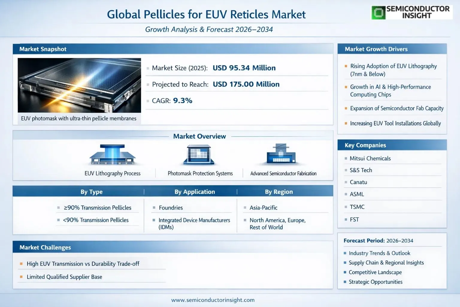
Global Pellicles for EUV Reticles market size was valued at USD 95.34 million in 2025. The market is projected to grow from USD 104.20 million in 2026 to USD 175.00 million by 2034, exhibiting a CAGR of 9.3% during the forecast period.
A pellicle for EUV reticles is a ultra-thin protective membrane used to shield a photomask from particulate contamination while permitting high transmission of extreme ultraviolet (EUV) light during the lithography process. It plays a critical role in advanced semiconductor manufacturing, where even nanometer-scale defects on the reticle surface can result in yield-impacting pattern errors. Initially designed as a single-layer structure with a core layer made of polysilicon, EUV pellicles have since evolved significantly. Since 2021, the industry has transitioned toward composite multi-layer architectures, incorporating alternating molybdenum disilicide (MoSi₂) and silicon (Si) layers. This structural advancement has elevated EUV transmittance (EUVT) , a key performance indicator , from approximately 82% to around 90%, meaningfully improving process efficiency.
The market is gaining strong momentum, driven by the accelerating adoption of EUV lithography in advanced chip manufacturing nodes of 7nm and below, where pattern sizes on the mask can reach only tens of nanometers, placing extremely strict requirements on pellicle uniformity and defect control. The next generation of high-power EUV lithography machines operates at more than 500W, further reinforcing the need for robust pellicle solutions to protect photomasks during high-volume production. Furthermore, the emergence of carbon nanotube (CNT) pellicle technology , developed through collaborations such as that between Canatu and imec since 2015 , signals a new material frontier beyond structural multi-layer improvements. Key players operating in this market include Mitsui Chemicals, S&S Tech, Canatu, TSMC, and FST, each advancing pellicle solutions tailored to the rigorous demands of next-generation EUV semiconductor fabrication.
MARKET DRIVERS
Accelerating Demand for Advanced Semiconductor Nodes Driving Pellicle Adoption
The rapid transition toward sub-5nm and sub-3nm semiconductor process nodes has emerged as a primary force shaping Pellicles for EUV Reticles Market. As chipmakers including leading foundries accelerate their roadmaps to deliver higher transistor density, the use of extreme ultraviolet lithography becomes indispensable. Pellicles serve as protective membranes placed over EUV reticles to prevent particulate contamination during the lithography process, and their role becomes increasingly critical as pattern dimensions shrink. The sensitivity of EUV reticles to even sub-20nm particles means that EUV pellicle technology directly determines yield outcomes at advanced nodes, compelling semiconductor manufacturers to invest heavily in pellicle-qualified production lines.
Expansion of EUV Lithography Tool Installations Worldwide
Global expansion of EUV scanner installations across semiconductor fabs in Asia-Pacific, North America, and Europe continues to generate sustained demand within Pellicles for EUV Reticles Market. Leading equipment suppliers have reported consistent growth in EUV system shipments, and each new tool installation necessitates a corresponding supply of qualified EUV pellicles. High-volume manufacturing environments require pellicle replacement at regular intervals, creating a recurring consumable demand that is structurally tied to the growing installed base of EUV lithography equipment. This dynamic reinforces a long-term, predictable demand trajectory for pellicle manufacturers capable of meeting the stringent transmission and durability requirements of high-throughput EUV fabs.
➤ The shift toward high numerical aperture (High-NA) EUV lithography represents a next-generation catalyst for Pellicles for EUV Reticles Market, as new optical architectures require pellicle designs with even greater EUV transmission efficiency and thermal stability, prompting accelerated R&D investment across the supply chain.
Government-backed semiconductor self-sufficiency initiatives across the United States, European Union, Japan, and South Korea are channeling significant capital into domestic fab construction projects. These investments directly stimulate demand for EUV reticle pellicles as newly commissioned fabs ramp up advanced node production. Strategic stockpiling of critical lithography consumables, including pellicles, has also become a supply chain priority following past disruptions, further amplifying near-term procurement volumes and supporting market revenue growth.
MARKET CHALLENGES
Technical Barriers in Achieving High EUV Transmission Combined with Mechanical Durability
One of the most significant technical challenges confronting Pellicles for EUV Reticles Market is the simultaneous achievement of high EUV light transmission and sufficient mechanical robustness under fab operating conditions. EUV pellicles must maintain transmission rates that avoid unacceptable throughput penalties while withstanding intense EUV radiation, thermal loading from the plasma light source, and the mechanical stresses of reticle handling. Materials such as polysilicon and silicon nitride thin films have been explored extensively, but each presents trade-offs between optical performance and structural integrity. Pellicle lifetime under high-power EUV exposure remains a persistent engineering challenge that constrains qualification timelines and limits the operational duty cycle achievable in production environments.
Other Challenges
Limited Qualified Supplier Base
The highly specialized nature of EUV pellicle manufacturing has resulted in a concentrated supplier landscape with only a small number of companies capable of producing pellicles that meet leading-edge fab qualification criteria. This limited supply base creates procurement risk for semiconductor manufacturers and can result in supply constraints during periods of rapid demand growth. Diversifying the qualified supplier ecosystem requires substantial capital investment in thin-film deposition infrastructure and extended qualification programs that can span multiple years.
High Cost of Pellicle Qualification and Integration
Qualifying a new EUV pellicle design within an active production fab involves extensive process integration testing, reticle compatibility validation, and lithographic performance characterization. The cost and time associated with these qualification cycles represent a meaningful barrier for both pellicle suppliers seeking to introduce improved products and for fabs considering supplier transitions. The economic burden of qualification, combined with the risk of yield excursions during integration, tends to create inertia around existing qualified solutions even when technically superior alternatives become available.
MARKET RESTRAINTS
Operational Constraints Arising from Pellicle-Induced EUV Throughput Reduction
A fundamental restraint affecting broader adoption within Pellicles for EUV Reticles Market is the throughput reduction associated with pellicle use. Because even state-of-the-art EUV pellicles absorb a portion of incident EUV radiation, their deployment reduces scanner throughput relative to pellicleless operation. For cost-sensitive production layers where contamination risk is managed through alternative means, some fabs have historically chosen to operate without pellicles on certain reticles, limiting total market penetration. As the industry moves toward higher EUV source power and High-NA platforms, transmission efficiency improvements in next-generation pellicle materials will be necessary to remove this throughput penalty as a commercial barrier.
Supply Chain Complexity and Raw Material Constraints for Advanced Pellicle Films
The fabrication of EUV pellicles relies on ultra-thin membranes produced from advanced materials including single-crystal silicon, polysilicon, and emerging carbon-based films such as carbon nanotube composites. The availability of suitable precursor materials with the purity and structural consistency required for pellicle-grade applications is constrained by a narrow base of qualified material suppliers. Disruptions in the supply of these specialty materials, or quality deviations at the raw material level, can propagate into pellicle manufacturing yield losses and delivery delays. This supply chain vulnerability represents a structural restraint on the ability of the EUV pellicle supply chain to scale in proportion with rapidly growing fab demand.
MARKET OPPORTUNITIES
Emergence of High-NA EUV Lithography Creating Next-Generation Pellicle Development Opportunities
The commercial introduction of High-NA EUV lithography systems opens a significant opportunity horizon for Pellicles for EUV Reticles Market. High-NA platforms operate with modified optical configurations that impose new pellicle form factor and transmission requirements distinct from those of conventional EUV tools. Pellicle suppliers that invest proactively in High-NA compatible designs stand to capture early qualification slots with leading-edge chipmakers, establishing a strong competitive position ahead of broader High-NA volume ramp. The development of next-generation pellicle membranes optimized for High-NA wavelength and incidence angle characteristics represents one of the most strategically valuable areas of innovation within the broader EUV lithography ecosystem.
Carbon Nanotube and Novel Membrane Materials Offering Breakthrough Transmission Performance
Research and development activity centered on carbon nanotube (CNT) pellicle membranes has demonstrated the potential to significantly exceed the EUV transmission levels achievable with conventional silicon-based films. CNT pellicle architectures offer a compelling combination of high optical transmission, low areal density, and thermal conductivity properties that address key limitations of incumbent materials. Successful commercialization of CNT-based EUV pellicles would represent a transformative development for the market, enabling pellicleless-equivalent throughput while maintaining contamination protection. Investment in this technology by both established pellicle manufacturers and new entrants reflects the magnitude of the commercial opportunity associated with achieving a materials breakthrough in EUV pellicle performance.
Geographic Diversification of Semiconductor Manufacturing Expanding Addressable Market Reach
The geographic broadening of advanced semiconductor manufacturing capacity across multiple regions presents a structural opportunity to expand the total addressable market for EUV reticle pellicles. New fab projects announced or under construction in the United States, Germany, Japan, and India introduce additional demand centers beyond the historically concentrated Asia-Pacific supply chain. Regional pellicle supply strategies, including the establishment of localized manufacturing or distribution capabilities, could allow pellicle suppliers to reduce logistics lead times, comply with emerging domestic content requirements, and build strategic partnerships with regional fab operators. This geographic diversification trend is expected to support sustained long-term volume growth across Pellicles for EUV Reticles Market through the latter half of this decade.
Trends
Rising Adoption of EUV Lithography Driving Demand for Advanced Pellicles
Pellicles for EUV Reticles Market is experiencing significant momentum as semiconductor manufacturers accelerate their transition toward extreme ultraviolet (EUV) lithography for advanced chip manufacturing. The growing production of chips at 7nm and below process nodes has made EUV pellicles an indispensable component in photomask protection. As chipmakers increasingly rely on EUV processes to meet the demands of artificial intelligence, high-performance computing, and next-generation mobile platforms, the requirement for high-transmittance, durable pellicles has become more critical than ever. Next-generation high-power EUV lithography machines operating at above 500W further underscore the need for pellicles capable of withstanding intense photon exposure while shielding photomasks from particle contamination during chip production.
Other Trends
Transition from Single-Layer to Multi-Layer Pellicle Structures
One of the most defining material trends in Pellicles for EUV Reticles Market is the structural evolution from single-layer polysilicon pellicles to composite multi-layer architectures. Since 2021, EUV pellicles have increasingly adopted alternating molybdenum disilicide (MoSi₂) and silicon (Si) layers. This structural advancement has improved EUV transmittance (EUVT) from approximately 82% to around 90%, a critical performance leap that directly enhances lithography throughput and yield. Suppliers such as S&S Tech in South Korea have developed pellicles achieving transmittance rates exceeding 90%, reinforcing the industry’s shift toward higher-performance multi-layer solutions.
Emergence of Carbon Nanotube (CNT) Pellicle Technology
The next frontier in Pellicles for EUV Reticles Market is the development and commercialization of carbon nanotube (CNT) pellicles, which promise superior thermal durability, higher transmittance, and improved mechanical strength compared to conventional multi-layer films. Canatu, in collaboration with Imec since 2015, has been advancing CNT pellicle technology to meet stringent performance targets including lifetime, transmittance, thermal resilience, permeability, and structural strength. Mitsui Chemicals, which holds a license from ASML for EUV pellicle technology and has been engaged in mass sales since 2021, is expected to complete its next-generation CNT pellicle production facility by the end of 2025, signaling a pivotal shift in manufacturing capacity for this emerging technology segment.
Geographic and Competitive Landscape Shaping Market Dynamics
Pellicles for EUV Reticles Market is characterized by a concentrated competitive landscape with key participants including Mitsui Chemicals, S&S Tech, Canatu, TSMC, and FST. Asia remains the dominant region for both production and consumption, driven by the concentration of leading foundries and integrated device manufacturers (IDMs) in South Korea, Japan, Taiwan, and China. The foundry segment, in particular, accounts for a substantial share of pellicle consumption as leading contract chipmakers scale up EUV-based production. Meanwhile, ongoing research and development investments by market participants to extend pellicle lifetime, improve defect control at sub-10nm pattern dimensions, and qualify CNT-based films for high-volume manufacturing continue to define the strategic direction of Pellicles for EUV Reticles Market.
COMPETITIVE LANDSCAPE
Key Industry Players
Pellicles for EUV Reticles Market , Competitive Dynamics, Strategic Positioning, and Key Manufacturer Profiles
The global Pellicles for EUV Reticles market is characterized by a concentrated competitive structure, with a handful of highly specialized players driving innovation and supply. ASML, the dominant force in EUV lithography equipment, pioneered the commercialization of EUV pellicles, launching its first product in 2019 before licensing the technology to Mitsui Chemicals, which subsequently commenced mass sales in 2021. This strategic licensing arrangement effectively positioned Mitsui Chemicals as the primary commercial supplier of EUV pellicles, giving it a significant first-mover advantage in a market valued at approximately USD 95.34 million in 2025 and projected to reach USD 175 million by 2034, growing at a CAGR of 9.3%. The market’s evolution from single-layer polysilicon structures to advanced multi-layer molybdenum disilicide (MoSi₂) and silicon composite membranes , boosting EUV transmittance from ~82% to ~90% , has raised the technological bar considerably, making R&D capability and materials expertise critical competitive differentiators.
Beyond the dominant players, a number of niche but strategically significant companies are actively shaping the competitive landscape. South Korean firm S&S Tech emerged as a notable challenger in 2021, developing a pellicle with transmittance exceeding 90%, targeting both IDM and foundry segments across Asia. Finnish deep-tech company Canatu has been collaborating with imec since 2015 to pioneer carbon nanotube (CNT)-based pellicle technology, widely regarded as the next-generation solution for high-power EUV systems operating above 500W. TSMC, as both a key end-user and an active technology development participant, maintains a strategic role in driving pellicle performance requirements. FST continues pellicle development activities, though its EUV-grade product remains in advanced development stages. The competitive intensity is expected to increase as chipmakers accelerate adoption of sub-7nm EUV processes and demand pellicles with superior thermal durability, defect control, and transmittance uniformity to support next-generation high-volume semiconductor manufacturing.
List of Key Pellicles for EUV Reticles Companies Profiled
- Mitsui Chemicals
- S&S Tech
- Canatu
- ASML
- TSMC
- FST (Fine Semitech)
- Shin-Etsu Chemical
- Toppan Photomasks
- Hoya Corporation
- Samsung Electronics
- Intel Corporation
- imec
- SK Hynix
- Entegris
- Advanced Energy Industries
Segment Analysis:
| Segment Category | Sub-Segments | Key Insights |
| By Type |
|
≥90% Transmission Rate Pellicles represent the leading and most strategically significant segment within Pellicles for EUV Reticles Market, driven by the semiconductor industry’s relentless push toward sub-7nm process nodes.
|
| By Application |
|
Foundry segment holds a commanding position in Pellicles for EUV Reticles Market, underpinned by the accelerating adoption of EUV lithography processes among leading contract chip manufacturers serving diverse and high-volume customer bases.
|
| By End User |
|
Logic Chip Manufacturers constitute the dominant end-user segment in Pellicles for EUV Reticles Market, driven by the critical reliance of advanced logic chip production on EUV lithography to achieve the miniaturization demanded by modern computing and AI applications.
|
| By Material Technology |
|
Multi-Layer MoSi₂/Si Composite Pellicles currently lead this segment, representing the industry-standard solution that succeeded single-layer polysilicon membranes as the dominant pellicle architecture following widespread commercial adoption from 2021 onward.
|
| By EUV Lithography Generation |
|
Standard EUV Pellicles currently dominate commercial demand as the established solution deployed across existing EUV lithography infrastructure in volume production environments, though the horizon is rapidly shifting toward next-generation requirements.
|
Regional Analysis: Pellicles for EUV Reticles Market
Asia-Pacific
Taiwan and South Korea remain at the forefront of EUV lithography adoption, with leading foundries and memory chipmakers deploying advanced EUV scanners at scale. This drives consistent procurement of pellicles for EUV reticles to ensure reticle integrity and yield optimization. Both nations benefit from strong government support, highly skilled semiconductor workforces, and deep collaboration with global EUV equipment and materials suppliers, reinforcing their market leadership.
Japan’s role in Pellicles for EUV Reticles Market is anchored in its world-class capabilities in advanced materials science and photomask technology. Japanese suppliers contribute critical components and raw materials essential to EUV pellicle manufacturing. Ongoing collaboration between domestic research institutions and global semiconductor firms supports continued innovation in pellicle membrane durability, transmittance, and contamination resistance, cementing Japan’s indispensable position in the regional supply chain.
China’s strategic ambition to achieve semiconductor self-reliance is generating growing interest in EUV-compatible pellicle solutions. State-sponsored programs and significant capital investment in domestic chipmakers are accelerating demand for advanced lithography consumables, including pellicles for EUV reticles. While access to leading-edge EUV tools remains constrained by geopolitical factors, China’s long-term trajectory points toward increased participation in the regional pellicle demand landscape.
Asia-Pacific benefits from a highly integrated semiconductor supply chain that spans materials sourcing, pellicle fabrication, photomask production, and wafer processing. This end-to-end ecosystem reduces lead times and facilitates rapid technology transfer between pellicle developers and chipmakers. The density of EUV-equipped fabs across the region ensures a robust and recurring demand base for pellicles for EUV reticles, supporting long-term commercial viability for regional and global suppliers alike.
North America
North America represents a strategically significant region in Pellicles for EUV Reticles Market, propelled by the United States’ ongoing reinvestment in domestic semiconductor manufacturing capacity. Legislative initiatives such as the CHIPS and Science Act have catalyzed a new wave of advanced fab construction across states including Arizona, Ohio, and New York. As these facilities reach operational maturity and begin deploying EUV lithography tools, demand for pellicles for EUV reticles is expected to rise meaningfully. The United States also hosts a concentration of leading semiconductor equipment companies, research universities, and national laboratories engaged in EUV materials research, contributing to the innovation pipeline. North American chipmakers are increasingly prioritizing supply chain resilience, which is encouraging closer partnerships with domestic and allied-nation pellicle suppliers. This strategic realignment is expected to shape procurement patterns in Pellicles for EUV Reticles Market throughout the 2026 to 2034 forecast window.
Europe
Europe occupies a unique and influential position in the global pellicles for EUV reticles market, primarily due to the presence of ASML in the Netherlands , the world’s sole manufacturer of EUV lithography systems. This concentration of EUV expertise creates a naturally supportive environment for adjacent technologies, including pellicle development and testing. European research consortia and publicly funded semiconductor programs are advancing materials innovation relevant to EUV pellicle performance. Countries such as Germany, Belgium, and the Netherlands maintain active involvement in photomask and reticle-related research. The European Chips Act is further stimulating regional semiconductor ambitions, with planned investments in advanced node fabrication that will necessitate EUV-compatible consumables. While Europe’s share of active EUV wafer production currently trails Asia-Pacific, the region’s intellectual contributions and equipment ecosystem make it a critical participant in Pellicles for EUV Reticles Market value chain.
South America
South America currently represents an emerging and nascent segment within the global pellicles for EUV reticles market. The region lacks a mature semiconductor fabrication base, and widespread adoption of EUV lithography technology remains a longer-term prospect. However, countries such as Brazil are making incremental investments in electronics manufacturing and semiconductor design capabilities, laying foundational groundwork for eventual participation in advanced chip production ecosystems. Government-led technology development programs and growing interest in attracting foreign direct investment to the electronics sector may gradually elevate South America’s relevance in the broader semiconductor supply chain. For the foreseeable forecast period, South America’s contribution to pellicle demand will remain limited, though monitoring evolving policy frameworks and industrial development initiatives will be important for long-term market participants tracking Pellicles for EUV Reticles Market.
Middle East & Africa
The Middle East and Africa region is at an early stage of engagement with Pellicles for EUV Reticles Market. While the region does not currently host significant EUV semiconductor manufacturing activity, certain Middle Eastern economies , particularly those within the Gulf Cooperation Council , are exploring technology diversification strategies as part of broader economic transformation agendas. Investments in semiconductor design, chip packaging, and advanced electronics assembly are beginning to take shape in countries such as the United Arab Emirates and Saudi Arabia. Africa’s semiconductor footprint remains minimal, though talent development programs and digital infrastructure investments signal future potential. Over the 2026 to 2034 period, the Middle East and Africa are unlikely to become major consumers of pellicles for EUV reticles, yet ongoing technology investment and strategic partnerships with global semiconductor leaders could position select markets within the region for gradual integration into the global EUV supply ecosystem.
Report Scope
This market research report provides a comprehensive analysis of Pellicles for EUV Reticles Market, covering the forecast period 2026–2034. It offers detailed insights into market dynamics, technological advancements, competitive landscape, and key trends shaping the industry.
Key focus areas of the report include:
- Market Overview: The report begins with an overview outlining its current market scenario, key growth indicators, and industry transformation drivers. It discusses macroeconomic factors, demand–supply balance, regulatory landscape, and the strategic role of semiconductors in powering advancements across industries such as automotive, telecommunications, consumer electronics, and industrial automation.
- Market Size & Forecast: Historical data and future projections for revenue, unit shipments, and market value across major regions and segments.
- Segmentation Analysis: Detailed breakdown by product type, technology, application, and end-user industry to identify high-growth segments and investment opportunities.
- Regional Insights: Insights into market performance across North America, Europe, Asia-Pacific, Latin America, and the Middle East & Africa, including country-level analysis where relevant.
- Competitive Landscape: Profiles of leading market participants, including their product offerings, R&D focus, manufacturing capacity, pricing strategies, and recent developments such as mergers, acquisitions, and partnerships.
- Technology Trends & Innovation: Assessment of emerging technologies, integration of AI/IoT, semiconductor design trends, fabrication techniques, and evolving industry standards.
- Market Drivers & Restraints: Evaluation of factors driving market growth along with challenges, supply chain constraints, regulatory issues, and market-entry barriers.
- Stakeholder Insights: Insights for component suppliers, OEMs, system integrators, investors, and policymakers regarding the evolving ecosystem and strategic opportunities.
Primary and secondary research methods are employed, including interviews with industry experts, data from verified sources, and real-time market intelligence to ensure the accuracy and reliability of the insights presented.
FREQUENTLY ASKED QUESTIONS:
What is the current market size of Pellicles for EUV Reticles Market?
-> Global Pellicles for EUV Reticles Market was valued at USD 95.34 million in 2025 and is expected to reach USD 175 million by 2034, growing at a CAGR of 9.3% during the forecast period.
Which key companies operate in Pellicles for EUV Reticles Market?
-> Key players include Mitsui Chemicals, S&S Tech, Canatu, TSMC, and FST, among others.
What are the key growth drivers?
-> Key growth drivers include rising adoption of EUV lithography in advanced chip manufacturing (7nm and below), growing demand for AI and high-performance computing chips, and the need to protect photomasks from particle contamination in high-power EUV lithography machines operating at over 500W.
Which region dominates the market?
-> Asia is the dominant and fastest-growing region, led by countries such as China, Japan, South Korea, and Southeast Asia, driven by the rapid expansion of semiconductor fabrication and chipmakers increasingly adopting EUV processes in advanced manufacturing.
What are the emerging trends?
-> Emerging trends include transition from single-layer polysilicon pellicles to multi-layer MoSi²/Si composite structures increasing EUV transmittance from ~82% to ~90%, and the development of next-generation carbon nanotube (CNT) pellicles offering superior thermal durability, permeability, and strength for future EUV lithography applications.

Get Sample Report PDF for Exclusive Insights
Report Sample Includes
- Table of Contents
- List of Tables & Figures
- Charts, Research Methodology, and more...