PCVD (Plasma Chemical Vapor Deposition) Market Insights
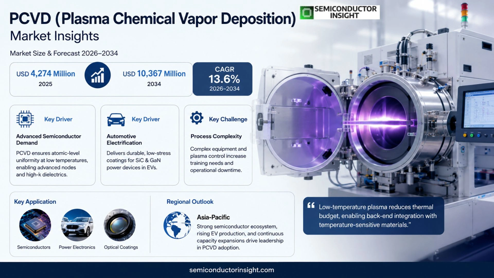
PCVD (Plasma Chemical Vapor Deposition) market was valued at USD 4,274 million in 2025 and will increase to USD 10,367 million by 2034, showing a CAGR of 13.6% over the forecast period.
PCVD, or Plasma Chemical Vapor Deposition, refers to a family of thin‑film deposition processes that employ radio‑frequency or other plasma sources to activate precursor gases. The activated species enable formation of dielectric layers, passivation films, hard masks, barrier coatings and selected amorphous silicon films on substrates such as wafers, glass, metals, ceramics or three‑dimensional parts while keeping substrate temperatures relatively low.
The sector is expanding because semiconductor manufacturers seek lower thermal budgets and higher film uniformity for advanced packaging and three‑dimensional integration. Leading suppliers,including Applied Materials, ASM International, Oxford Instruments and NAURA,have announced new low‑temperature PECVD platforms targeting 300 mm high‑throughput lines in early 2024. Meanwhile firms such as KLA and SAMCO are emphasizing process‑package bundles that combine PECVD tools with defect‑inspection services for MEMS and photonic devices. These initiatives reflect a shift from pure equipment sales toward integrated solutions that address film stress control, edge profile consistency and downstream compatibility.
MARKET DRIVERS
Advanced Semiconductor Demand
The relentless push toward sub‑10 nm logic devices forces chipmakers to adopt deposition techniques that deliver atomic‑level uniformity. PCVD (Plasma Chemical Vapor Deposition) meets this requirement by generating high‑density plasma at relatively low substrate temperatures, preserving delicate gate stacks while still producing dense films. This capability is reshaping process windows for high‑k dielectrics and metal gates, where any variation directly impacts yield.
Automotive Electrification
Electric‑vehicle powertrains rely on power electronics that must operate under harsh thermal cycles and exposure to salts. PCVD’s ability to deposit wear‑resistant, low‑stress coatings on silicon carbide and gallium nitride substrates gives OEMs a pathway to extend component life without resorting to bulky heat‑sink designs. Consequently, suppliers are integrating PCVD modules into assembly lines that serve both consumer‑grade and automotive‑grade markets.
➤ “The low‑temperature plasma environment reduces thermal budget, enabling back‑end integration with temperature‑sensitive materials.”
Beyond chips and vehicles, the optical coating sector is leveraging PCVD to fabricate antireflective layers for advanced lenses. The technique’s precision translates into higher optical performance, which in turn fuels demand from medical imaging and augmented‑reality manufacturers that cannot compromise on throughput.
MARKET CHALLENGES
Process Complexity
PCVD equipment integrates RF generators, intricate gas‑handling manifolds, and real‑time plasma diagnostics. Operators must master plasma chemistry while managing rapid cycle times, a combination that inflates both training costs and downtime. Manufacturers that lack dedicated engineering teams often face steep learning curves, limiting the technology’s adoption in smaller fabs.
Other Challenges
Regulatory Compliance
Environmental regulations governing fluorinated precursors and by‑products tighten in major regions. Companies must install abatement systems and conduct continuous emissions monitoring, adding layers of capital expense and procedural overhead that can deter entry‑level players.
MARKET RESTRAINTS
High Equipment Costs
State‑of‑the‑art PCVD reactors command multi‑million‑dollar price tags, a figure that strains capital budgets for emerging fabs. The return on investment hinges on sustained high‑volume production; any fluctuation in demand can stretch payback periods beyond acceptable thresholds for many investors.
MARKET OPPORTUNITIES
Emerging Flexible Electronics
Wearable health monitors and roll‑to‑fit displays demand deposition on polymeric substrates that cannot endure traditional high‑temperature processes. PCVD’s low‑temperature plasma chemistry enables conformal barrier layers on bends and folds, opening a niche where conventional CVD methods falter. Early adopters that establish supply chains for flexible PCVD tooling stand to capture a growing share of the next‑generation consumer electronics market.
PCVD (Plasma Chemical Vapor Deposition) Market Trends
Shift Toward Integrated Platform Value
PCVD (Plasma Chemical Vapor Deposition) Market has moved beyond pure film‑formation capability. Suppliers now package the tool with process recipes, upgrade paths, and on‑site service teams to guarantee that a specific dielectric stack can be delivered within a tight thermal budget. This transition is driven by three‑dimensional chip architectures, where film stress, defect density, and edge profile directly affect yield. Customers therefore evaluate a purchase on the basis of total‑system throughput and consistency rather than raw deposition rate. The shift has already raised the average contract size, because manufacturers bundle hardware with long‑term process support, creating a more predictable revenue stream for equipment makers.
Other Trends
Emerging Applications in Energy and Photonics
Research laboratories and pilot lines are expanding the use of plasma‑based deposition to thin‑film photovoltaics, large‑area transparent conductors, and photonic waveguides. Low‑temperature PECVD enables functional carbon and silicon nitride layers on flexible substrates that cannot survive conventional furnace cycles. This has opened a niche where equipment volume is modest but margins are attractive, as end users seek rapid iteration cycles and short time‑to‑market. The same capability is being leveraged for heterojunction solar cells, where a high‑quality passivation layer deposited at ≤200 °C improves cell efficiency without compromising substrate integrity. Consequently, the demand base is no longer limited to hyperscale fabs; it now includes specialty‑volume producers and OEMs of optical components.
Regional Concentration and Competitive Landscape
Manufacturing capacity for PCVD tools remains clustered in the United States, Japan, South Korea, and China, while the bulk of capital spending is concentrating in Asian advanced‑packaging hubs. The escalation of AI‑driven server chips and high‑bandwidth memory has heightened the need for low‑damage dielectric layers, reinforcing the relevance of high‑throughput 300 mm platforms. Established vendors such as Applied Materials, ASM International, and KLA retain leadership in high‑end single‑wafer and cluster systems, backed by long‑term customer qualification programs. Chinese equipment makers are gaining traction by offering rapid iteration cycles, localized support, and competitive pricing, allowing them to capture a growing share of the regional spend. The competitive dynamic is therefore evolving into a dual track: premium players focus on breakthrough film stacks for leading‑edge logic, while cost‑effective manufacturers target the expanding middle‑tier and research segments.
COMPETITIVE LANDSCAPE
Key Industry Players
PCVD Market – Competitive Overview
Applied Materials continues to shape the PCVD arena through its expansive portfolio that couples low‑temperature plasma sources with high‑throughput wafer‑scale platforms. The company leverages its deep relationships with leading foundries to embed deposition tools within end‑to‑end process flows, emphasizing film‑stress control, defect mitigation, and seamless hand‑off to downstream etch and bonding stages. This systems‑focused approach translates into recurring revenue streams from upgrades, process licences, and on‑site service contracts, reinforcing Applied Materials’ position as the benchmark for large‑volume, advanced‑packaging customers.
Beyond the headline makers, a cluster of specialised vendors fuels diversification across applications. Oxford Instruments and SENTECH Instruments excel in niche research and MEMS segments, offering batch‑type and custom‑geometry reactors prized for their flexibility. KLA’s recent entry into plasma‑diagnostics‑enabled deposition underscores a trend toward integrated metrology that shortens qualification cycles. Meanwhile, firms such as Denton Vacuum and SAMCO provide cost‑effective single‑wafer solutions targeting mid‑size fabs and photovoltaic manufacturers, allowing them to adopt low‑budget PCVD routes without sacrificing film uniformity. This mosaic of capabilities creates a layered competitive structure where high‑end platform providers coexist with agile specialists catering to emerging device categories.
List of Key PCVD Companies Profiled
- Applied Materials, Inc.
- Lam Research Corporation
- ASM International N.V.
- Oxford Instruments plc
- KLA Corporation
- SENTECH Instruments GmbH
- Plasma‑Therm LLC
- Denton Vacuum LLC
- ACM Research, Inc.
- ULVAC, Inc.
- SAMCO Inc.
- Sumitomo Precision Products Co., Ltd.
- WONIK IPS Co., Ltd.
- JUSUNG ENGINEERING Co., Ltd.
- NAURA Technology Group Co., Ltd.
Segment Analysis:
| Segment Category | Sub-Segments | Key Insights |
| By Type |
|
RF Plasma
|
| By Application |
|
Integrated Circuits and Advanced Packaging
|
| By End User |
|
Foundries
|
| By Process Advantage |
|
Low‑Temperature Processing
|
| By Market Dynamics |
|
Platform‑Level Competition
|
Regional Analysis: PCVD (Plasma Chemical Vapor Deposition) Market
Asia-Pacific
Displays, power electronics, and MEMS devices are each exploring plasma‑enhanced layers to achieve tighter tolerances, prompting equipment makers to tailor reactors for niche thickness regimes and material stacks.
Localized sourcing of high‑purity gases and precision quartz components reduces lead times, allowing manufacturers to respond to market fluctuations without extensive inventory buffers.
Harmonized safety standards across China, Japan, and Korea simplify cross‑border equipment certification, encouraging multinational collaborations on process development.
Venture capital groups targeting clean‑tech and advanced manufacturing have earmarked a growing share of their portfolios for plasma‑based process innovators.
North America
North America remains a hub for high‑value research, where university labs and corporate R&D centers co‑develop plasma chemistries aimed at automotive and aerospace sectors. The continent’s robust IP framework gives firms confidence to invest in proprietary deposition recipes, while a mature customer base seeks equipment that can integrate with existing fabs. Strategic alliances between equipment vendors and semiconductor giants are reshaping the value chain, prompting a shift toward modular reactor designs that can be reconfigured for multiple product lines. Although cost pressures are evident, the emphasis on reliability and long‑term service contracts sustains a premium market segment for advanced PCVD (Plasma Chemical Vapor Deposition) solutions.
Europe
European players leverage strong environmental regulations to promote greener plasma processes, replacing hazardous wet‑chemistry steps with dry‑film alternatives. The region’s industrial clusters in Germany and the Benelux nations foster collaborative pilots that test equipment under real‑world production conditions. Policy incentives for low‑carbon manufacturing encourage manufacturers to adopt plasma techniques that lower energy consumption. Consequently, equipment suppliers are tailoring system architectures to meet stringent emission standards, creating a niche where compliance and performance intersect.
South America
In South America, emerging semiconductor assembly lines are beginning to explore plasma deposition as a means to enhance yield without massive capital outlay. Local governments are offering tax relief for technology upgrades, which spurs interest among midsized producers. The market narrative is shifting from cost avoidance to value creation, as firms recognize the role of refined thin‑film layers in extending product lifecycles. Partnerships with Asian equipment makers provide access to calibrated tools, accelerating the region’s learning curve.
Middle East & Africa
The Middle East & Africa region is gradually positioning itself as a downstream processing hub, capitalizing on inexpensive energy and strategic ports. Pilot projects in solar‑cell fabrication are experimenting with plasma‑based passivation layers to boost efficiency. While the ecosystem is still nascent, joint ventures with established Asian vendors deliver technical know‑how, and regional investment funds are earmarking capital for clean‑technology manufacturing corridors. This early‑stage activity hints at a longer‑term shift toward higher value‑added production within PCVD (Plasma Chemical Vapor Deposition) Market.
Report Scope
This market research report provides a comprehensive analysis of the PCVD (Plasma Chemical Vapor Deposition) Market , covering the forecast period 2026–2034. It offers detailed insights into market dynamics, technological advancements, competitive landscape, and key trends shaping the industry.
Key focus areas of the report include:
- Market Overview: The report begins with an overview outlining its current market scenario, key growth indicators, and industry transformation drivers. It discusses macroeconomic factors, demand–supply balance, regulatory landscape, and the strategic role of semiconductors in powering advancements across industries such as automotive, telecommunications, consumer electronics, and industrial automation.
- Market Size & Forecast: Historical data and future projections for revenue, unit shipments, and market value across major regions and segments.
- Segmentation Analysis: Detailed breakdown by product type, technology, application, and end-user industry to identify high-growth segments and investment opportunities.
- Regional Insights: Insights into market performance across North America, Europe, Asia-Pacific, Latin America, and the Middle East & Africa, including country-level analysis where relevant.
- Competitive Landscape: Profiles of leading market participants, including their product offerings, R&D focus, manufacturing capacity, pricing strategies, and recent developments such as mergers, acquisitions, and partnerships.
- Technology Trends & Innovation: Assessment of emerging technologies, integration of AI/IoT, semiconductor design trends, fabrication techniques, and evolving industry standards.
- Market Drivers & Restraints: Evaluation of factors driving market growth along with challenges, supply chain constraints, regulatory issues, and market-entry barriers.
- Stakeholder Insights: Insights for component suppliers, OEMs, system integrators, investors, and policymakers regarding the evolving ecosystem and strategic opportunities.
Primary and secondary research methods are employed, including interviews with industry experts, data from verified sources, and real-time market intelligence to ensure the accuracy and reliability of the insights presented.
FREQUENTLY ASKED QUESTIONS:
What is the current market size of PCVD (Plasma Chemical Vapor Deposition) Market?
-> PCVD (Plasma Chemical Vapor Deposition) market will increase to USD 10,367 million by 2034, showing a CAGR of 13.6% over the forecast period.
Which key companies operate in PCVD (Plasma Chemical Vapor Deposition) Market?
-> Key players include Applied Materials, Inc.; Lam Research Corporation; ASM International N.V.; Oxford Instruments plc; KLA Corporation; SENTECH Instruments GmbH; Plasma‑Therm LLC; Denton Vacuum LLC; CVD Equipment Corporation; ACM Research, Inc.; ULVAC, Inc.; SAMCO Inc.; Sumitomo Precision Products Co., Ltd.; WONIK IPS Co., Ltd.; JUSUNG ENGINEERING Co., Ltd.; TES Co., Ltd.; NAURA Technology Group Co., Ltd.; Piotech Inc.; SKY Technology Development Co., Ltd.; NOBODY Materials Science & Technology Co., Ltd.; Syskey Technology Co., Ltd.; Dah Young Vacuum Equipment Co., Ltd..
What are the key growth drivers?
-> Key growth drivers include the rapid expansion of advanced packaging and 3D integration, increasing demand for low‑temperature, low‑damage dielectric films in AI‑driven server and high‑bandwidth memory production, growth of power and compound semiconductor applications, rising MEMS and photonic device volumes, and the broadened use of PCVD for photovoltaic and large‑area thin‑film solutions.
Which region dominates the market?
-> Asia‑Pacific dominates the PCVD market, driven by concentrated semiconductor fab and advanced packaging investments in China, Japan, South Korea, and Taiwan, which together account for the largest share of equipment consumption.
What are the emerging trends?
-> Emerging trends include the shift toward low‑temperature high‑throughput single‑wafer and cluster platforms, integration of PCVD within heterogeneous integration and advanced packaging process chains, development of DLC and low‑k dielectric solutions for energy‑related applications, and the increasing competitive presence of Chinese suppliers offering faster iteration and cost‑effective local service.

Get Sample Report PDF for Exclusive Insights
Report Sample Includes
- Table of Contents
- List of Tables & Figures
- Charts, Research Methodology, and more...
 Download Sample Report PDF