
Patterned Wafer Optical Defect Inspection Equipment Market Insights
Global Patterned Wafer Optical Defect Inspection Equipment market size was valued at USD 2.80 billion in 2026. The market is projected to grow from USD 3.05 billion in 2026 to USD 6.08 billion by 2034, exhibiting a CAGR of 9.0% during the forecast period.
Patterned Wafer Optical Defect Inspection Equipment comprises advanced optical systems vital for semiconductor manufacturing quality control. These tools detect microscopic defects on patterned wafers through non-contact, high-speed imaging, aiding yield improvement and process optimization amid chip miniaturization and complexity. Primary types include Bright Field Inspection Systems, suited for precise patterned wafer analysis due to stringent technical demands, and Dark Field Inspection Systems, differing in illumination and imaging principles.
The market experiences robust growth driven by surging semiconductor demand, advancements in AI, IoT, and advanced packaging, alongside China’s semiconductor testing sector eyeing a 14% CAGR over the next five years from policy support and localization efforts. While challenges like talent shortages persist, opportunities abound. Key players like KLA Corporation, Applied Materials, Hitachi High-Tech, Onto Innovation, and Wuhan Jingce Electronic Group dominate with innovative portfolios. For instance, domestic leader Wuhan Jingce Electronic Group has surged via indigenous tech and strategic mergers, bolstering global competition.
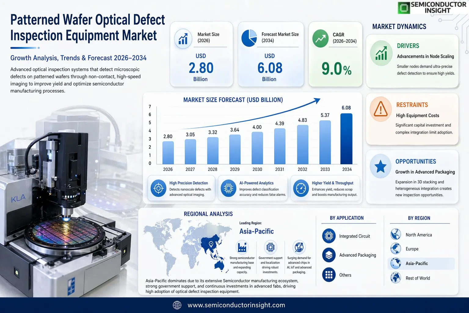
MARKET DRIVERS
Advancements in Semiconductor Node Scaling
Patterned Wafer Optical Defect Inspection Equipment Market is propelled by the relentless push toward smaller process nodes, such as 5nm and 3nm, demanding ultra-precise defect detection to ensure yield rates above 90% in high-volume manufacturing. Optical inspection systems leverage advanced illumination and imaging technologies to identify nanoscale defects on patterned wafers, directly supporting the semiconductor industry’s growth projected at a CAGR of 8.5% through 2030.
Integration of AI and Machine Learning
AI-driven algorithms enhance defect classification accuracy by up to 30%, reducing false positives and enabling real-time analysis in Patterned Wafer Optical Defect Inspection Equipment Market. This integration aligns with the surge in complex chip designs for AI chips and 5G infrastructure, where traditional methods fall short.
➤ Major foundries like TSMC and Samsung report 20-25% yield improvements using advanced optical inspection tools for EUV-patterned wafers.
Furthermore, rising demand for memory and logic devices amplifies the need for reliable inspection, fostering innovation in broadband plasma illumination for multi-layer defect visibility in Patterned Wafer Optical Defect Inspection Equipment Market.
MARKET CHALLENGES
Detecting Sub-10nm Defects
Identifying defects below 10nm on densely patterned wafers remains a core challenge in Patterned Wafer Optical Defect Inspection Equipment Market, as diffraction limits constrain optical resolution despite DUV and EUV enhancements. Throughput pressures in fabs handling 100,000+ wafers monthly exacerbate this issue.
Other Challenges
High Equipment Costs and Complexity
Capital expenditure for state-of-the-art systems exceeds $50 million per unit, straining budgets for mid-tier manufacturers and complicating integration with existing 300mm wafer lines in Patterned Wafer Optical Defect Inspection Equipment Market.Supply chain vulnerabilities for precision optics and sensors further delay deployments, with lead times stretching to 12-18 months amid global shortages.
MARKET RESTRAINTS
Capital Intensity and Economic Volatility
Patterned Wafer Optical Defect Inspection Equipment Market faces restraints from high upfront costs, often surpassing $100 million for full fab inspection suites, limiting adoption among smaller players. Economic downturns, like those impacting chip demand in 2023, reduce capex by 15-20%.Regulatory hurdles for cleanroom compliance and export controls on advanced tech slow market penetration, particularly in emerging regions.Dependence on a few suppliers for critical components, such as high-NA lenses, creates bottlenecks, restraining overall market expansion to a modest 7% CAGR in the near term.
MARKET OPPORTUNITIES
Expansion into Advanced Packaging
Growth in heterogeneous integration and 3D stacking opens avenues for specialized optical inspection in Patterned Wafer Optical Defect Inspection Equipment Market, with advanced packaging projected to capture 25% of semiconductor production by 2028.Emerging markets in Asia-Pacific, driven by new fabs in India and Vietnam, present untapped demand, potentially adding $2 billion in equipment sales over five years.Innovations in hyperspectral imaging and cloud-based analytics offer differentiation, enabling retrofit upgrades that boost resolution by 40% without full replacements.
Patterned Wafer Optical Defect Inspection Equipment Market Trends
Advancements in Optical Detection Technologies
Patterned Wafer Optical Defect Inspection Equipment Market is experiencing significant evolution driven by the ongoing miniaturization of chips and increasing complexity in semiconductor manufacturing processes. Optical defect inspection equipment plays a pivotal role in quality management, encompassing design, production, and detection to enhance wafer production yields, reduce costs, and optimize operational efficiency. This technology addresses system-level defects by precisely measuring transistor structures through advanced instruments, complemented by electrical testing for performance verification across the production lifecycle from design to final testing. Within this domain, optical detection stands out for its speed, non-contact nature, non-destructive approach, and seamless online integration, making it widely adopted in semiconductor fabrication for patterned wafers.
Other Trends
Expansion of Bright Field Inspection Systems
Bright field inspection systems within Patterned Wafer Optical Defect Inspection Equipment Market are gaining prominence due to their stringent technical requirements tailored specifically for defect detection on patterned wafers. Unlike dark field systems, which differ in illumination and imaging principles, bright field systems excel in capturing intricate details essential for advanced nodes. This shift supports the industry’s push towards higher precision as wafer patterns become more sophisticated, enabling manufacturers to maintain high yields amid escalating process complexities.
Rise of Domestic Players and Regional Opportunities in Asia
In Patterned Wafer Optical Defect Inspection Equipment Market, domestic enterprises such as Wuhan Jingce Electronic Group are rapidly ascending through endogenous technology development and strategic mergers, bolstered by national policies and demands for local substitution in key semiconductor testing segments. Asia, particularly China, presents optimistic development prospects fueled by supportive industrial environments, though challenges like talent shortages and supply chain maturation persist. The surge in applications for artificial intelligence, Internet of Things, and new energy vehicles further broadens opportunities, driving demand for reliable optical inspection solutions from leading global players including KLA Corporation, Applied Materials, and Hitachi High-Tech. These dynamics underscore a competitive landscape where innovation in optical systems aligns with global trends in integrated circuits and advanced packaging, ensuring sustained market growth through enhanced defect management capabilities.
COMPETITIVE LANDSCAPE
Key Industry Players
Top Players in Patterned Wafer Optical Defect Inspection Equipment Market
Patterned Wafer Optical Defect Inspection Equipment Market is dominated by a few established global leaders, with KLA Corporation holding the largest market share due to its comprehensive portfolio of advanced optical inspection systems, including bright field and dark field technologies tailored for patterned wafers. This oligopolistic structure features intense competition among top-tier players like Applied Materials and Hitachi High-Tech, who leverage integrated solutions for semiconductor yield enhancement. In 2026, the global top five players collectively commanded a significant revenue share, driven by demand in integrated circuits and advanced packaging applications. These leaders benefit from technological superiority in high-resolution, non-destructive detection, aligning with chip miniaturization trends and process complexity in semiconductor manufacturing.
Beyond the frontrunners, niche and emerging players contribute to market diversity, particularly in regional segments like Asia-Pacific. Companies such as Onto Innovation and ASML provide specialized metrology and inspection tools, while Chinese firms including Wuhan Jingce Electronic Group and Shanghai Micro Electronics Equipment are gaining traction through domestic substitution strategies and rapid technological advancements. Players like Skyverse Technology and Suzhou TZTEK Technology focus on cost-effective optical systems for bright field inspection, addressing system-level defects and supporting yield optimization. This competitive landscape reflects a blend of innovation-driven incumbents and agile challengers, with ongoing mergers, R&D investments, and expansions shaping future dynamics amid AI, IoT, and advanced packaging growth.
List of Key Patterned Wafer Optical Defect Inspection Equipment Companies Profiled
- KLA Corporation
- Applied Materials
- Hitachi High-Tech
- ASML
- Onto Innovation
- NanoSystem Solutions
- Skyverse Technology
- Wuhan Jingce Electronic Group
- RSIC
- Shanghai Micro Electronics Equipment
- Suzhou TZTEK Technology
- Camtek Ltd.
- Hermes Microvision (ASML)
- Toray Engineering
- Screen Holdings
Segment Analysis:
| Segment Category | Sub-Segments | Key Insights |
| By Type |
|
Bright Field Inspection System is the leading segment owing to its stringent technical requirements tailored for patterned wafer defect detection.
|
| By Application |
|
Integrated Circuit dominates as the primary application driving demand for optical defect inspection.
|
| By End User |
|
Semiconductor Foundries lead adoption due to their high-volume production needs.
|
| By Wafer Size |
|
300mm Wafers emerges as the frontrunner aligned with modern fabrication standards.
|
| By Process Node |
|
Advanced Nodes (Sub-10nm) commands leadership amid escalating complexity in chip design.
|
Regional Analysis: Patterned Wafer Optical Defect Inspection Equipment Market
Asia-Pacific
Innovation thrives in Asia-Pacific with integration of AI and machine learning into optical defect inspection systems, enabling precise detection of subtle pattern irregularities. Leading fabs adopt multi-beam laser scanning for enhanced resolution, addressing challenges in EUV lithography wafers. Collaborative R&D between equipment makers and chip producers accelerates deployment of adaptive algorithms, boosting throughput without sacrificing accuracy in high-mix production environments.
Global leaders like KLA-Tencor and Applied Materials maintain strong footprints, alongside regional giants such as Tokyo Electron. These firms offer tailored inspection platforms optimized for Asia-Pacific’s diverse node portfolios, from mature to advanced processes. Strategic partnerships with local foundries ensure rapid service response, fostering loyalty and market penetration amid fierce competition.
Favorable government policies, including subsidies for semiconductor infrastructure, encourage adoption of advanced patterned wafer optical defect inspection equipment. Export controls and domestic technology mandates stimulate local manufacturing of inspection tools, reducing reliance on imports. Standards for defect metrology align with international benchmarks, promoting seamless integration across global supply chains.
Escalating chip complexity and capacity expansions propel demand for sophisticated optical inspection solutions. The shift to heterogeneous integration heightens need for versatile systems capable of handling 3D structures. Rising fab utilization rates underscore the critical role of inspection in maintaining quality, positioning Asia-Pacific for continued dominance in the market.
North America
North America excels in innovation within Patterned Wafer Optical Defect Inspection Equipment Market, spearheaded by U.S.-based developers of cutting-edge optical technologies. Home to pioneering firms, the region emphasizes R&D for next-gen inspection platforms featuring hyperspectral imaging and deep learning analytics. Strong IP ecosystems and university collaborations drive breakthroughs in defect root-cause analysis, influencing global standards. While production volumes trail Asia-Pacific, North America’s focus on design and software enhancements supplies high-value systems worldwide. Investments in domestic fabs by tech giants further stimulate demand, balancing export-oriented growth with localized advancements amid supply chain diversification efforts.
Europe
Europe demonstrates steady growth in Patterned Wafer Optical Defect Inspection Equipment Market, bolstered by specialized semiconductor clusters in Germany, the Netherlands, and France. Research institutions advance optical metrology for patterned wafers, prioritizing sustainability and precision in defect detection. Regional players integrate inspection tools with smart manufacturing frameworks, enhancing yield in automotive and industrial chip production. EU-funded initiatives promote collaboration across borders, fostering adoption of AI-driven systems. Emphasis on regulatory compliance drives demand for traceable inspection processes, positioning Europe as a hub for high-reliability applications despite moderate fab capacities.
South America
South America represents an emerging landscape in Patterned Wafer Optical Defect Inspection Equipment Market, with Brazil leading nascent semiconductor efforts. Investments in electronics assembly and nascent fab developments spur interest in cost-effective optical inspection solutions for patterned wafers. Regional demand aligns with consumer electronics growth, focusing on mature nodes where defect management improves output quality. Partnerships with international suppliers facilitate technology transfer, building local expertise. Challenges like infrastructure gaps are offset by strategic incentives, laying groundwork for expanded utilization as the ecosystem matures.
Middle East & Africa
The Middle East & Africa region shows promising traction in Patterned Wafer Optical Defect Inspection Equipment Market, driven by diversification strategies in the UAE and Saudi Arabia. Sovereign wealth funds back new semiconductor ventures, incorporating advanced optical inspection for wafer patterning integrity. Africa’s growing tech hubs prioritize accessible systems for assembly operations, emphasizing ease of integration. Collaborative ventures with global experts bridge skill gaps, supporting defect-free production in emerging device fabrication. Geopolitical investments signal potential for accelerated adoption, enhancing regional resilience in electronics supply.
Report Scope
This market research report provides a comprehensive analysis of Patterned Wafer Optical Defect Inspection Equipment Market, covering the forecast period 2026–2032. It offers detailed insights into market dynamics, technological advancements, competitive landscape, and key trends shaping the industry.
Key focus areas of the report include:
- Market Overview: The report begins with an overview outlining its current market scenario, key growth indicators, and industry transformation drivers. It discusses macroeconomic factors, demand–supply balance, regulatory landscape, and the strategic role of semiconductors in powering advancements across industries such as automotive, telecommunications, consumer electronics, and industrial automation.
- Market Size & Forecast: Historical data and future projections for revenue, unit shipments, and market value across major regions and segments.
- Segmentation Analysis: Detailed breakdown by product type, technology, application, and end-user industry to identify high-growth segments and investment opportunities.
- Regional Insights: Insights into market performance across North America, Europe, Asia-Pacific, Latin America, and the Middle East & Africa, including country-level analysis where relevant.
- Competitive Landscape: Profiles of leading market participants, including their product offerings, R&D focus, manufacturing capacity, pricing strategies, and recent developments such as mergers, acquisitions, and partnerships.
- Technology Trends & Innovation: Assessment of emerging technologies, integration of AI/IoT, semiconductor design trends, fabrication techniques, and evolving industry standards.
- Market Drivers & Restraints: Evaluation of factors driving market growth along with challenges, supply chain constraints, regulatory issues, and market-entry barriers.
- Stakeholder Insights: Insights for component suppliers, OEMs, system integrators, investors, and policymakers regarding the evolving ecosystem and strategic opportunities.
Primary and secondary research methods are employed, including interviews with industry experts, data from verified sources, and real-time market intelligence to ensure the accuracy and reliability of the insights presented.
FREQUENTLY ASKED QUESTIONS:
What is the current market size of Patterned Wafer Optical Defect Inspection Equipment Market?
-> Global Patterned Wafer Optical Defect Inspection Equipment market was valued at USD million in 2026 and is projected to reach USD million by 2032, at a % CAGR during the forecast period.
Which key companies operate in Patterned Wafer Optical Defect Inspection Equipment Market?
-> Key players include KLA Corporation, Applied Materials, Hitachi High-Tech, ASML, Onto Innovation, NanoSystem Solutions, Skyverse Technology, Wuhan Jingce Electronic Group, RSIC, Shanghai Micro Electronics Equipment, among others.
What are the key growth drivers?
-> Key growth drivers include chip miniaturization, process complexity, national policy support, domestic substitution demand in China, and rise of artificial intelligence, Internet of Things, and new energy vehicles.
Which region dominates the market?
-> Asia, particularly China, is the fastest-growing region at a predicted 14% CAGR over the next five years, while the U.S. holds significant market share.
What are the emerging trends?
-> Emerging trends include optical detection advancements like bright field and dark field systems for patterned wafers, high-resolution electron beam inspection, non-contact non-destructive testing, and online integration for improved yield and efficiency.

Get Sample Report PDF for Exclusive Insights
Report Sample Includes
- Table of Contents
- List of Tables & Figures
- Charts, Research Methodology, and more...






