
MARKET INSIGHTS
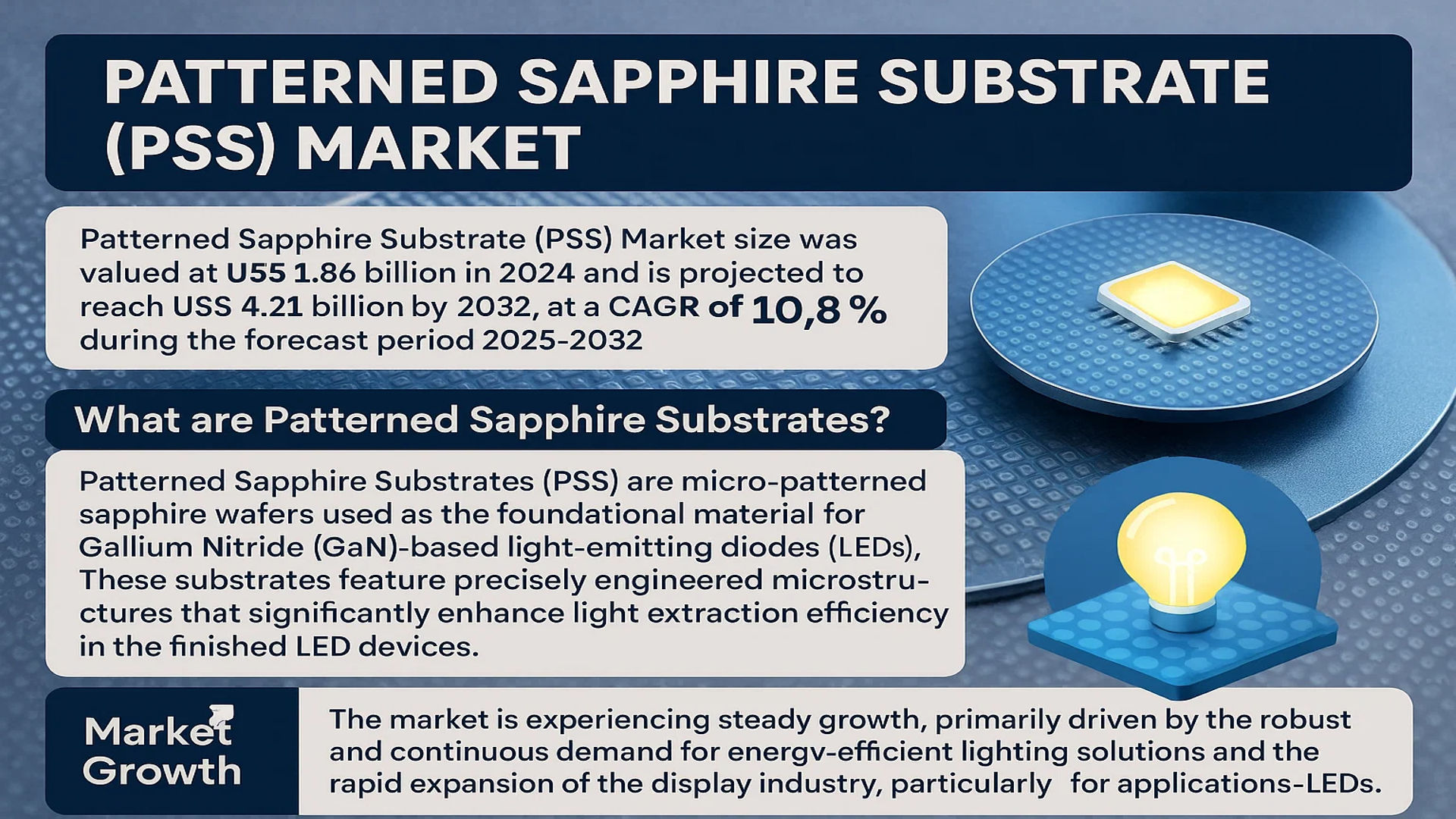
The global Patterned Sapphire Substrate (PSS) Market size was valued at US$ 1.86 billion in 2024 and is projected to reach US$ 4.21 billion by 2032, at a CAGR of 10.8% during the forecast period 2025-2032.
Patterned Sapphire Substrates (PSS) are micro-patterned sapphire wafers used as the foundational material for Gallium Nitride (GaN)-based light-emitting diodes (LEDs). These substrates feature precisely engineered microstructures that significantly enhance light extraction efficiency in the finished LED devices. Furthermore, PSS technology addresses critical challenges in LED manufacturing, including crystal dislocations and refractive index mismatch, which are paramount for achieving high brightness and performance.
The market is experiencing steady growth, primarily driven by the robust and continuous demand for energy-efficient lighting solutions and the rapid expansion of the display industry, particularly for applications like micro-LEDs. While the majority of PSS products are manufactured using dry plasma etching due to its superior precision and uniformity, the industry is also witnessing advancements in wet chemical etching processes. Key players such as CRYSCORE, Sanan Optoelectronics, and Huacan Semitek dominate the market, with the global top five players holding a collective revenue share of approximately 55% in 2024. The 4-inch substrate segment currently holds the largest market share, but the 6-inch segment is anticipated to witness the highest growth rate due to its cost-efficiency in high-volume production.
MARKET DYNAMICS
MARKET DRIVERS
Growing Demand for High-Efficiency LEDs to Drive Patterned Sapphire Substrate Adoption
The global push toward energy-efficient lighting solutions is significantly accelerating the demand for high-brightness LEDs, which extensively utilize Patterned Sapphire Substrates (PSS) to enhance light extraction efficiency. PSS technology addresses critical limitations in conventional LED manufacturing by reducing crystal dislocations and minimizing refractive index mismatches, resulting in up to 60% improvement in luminous efficacy compared to non-patterned substrates. The LED market, valued at approximately $75 billion globally, continues to expand due to governmental regulations phasing out inefficient lighting and increasing adoption in automotive, display, and general illumination applications. This sustained growth directly correlates with increased PSS consumption, particularly as manufacturers transition to larger wafer sizes to improve production economies.
Advancements in Manufacturing Technologies to Boost Market Growth
Technological innovations in dry plasma etching processes have revolutionized PSS production by enabling superior pattern uniformity and precision at nanoscale dimensions. The dominance of dry etching over wet chemical methods—accounting for over 85% of global PSS production—stems from its ability to create consistent patterns with aspect ratios exceeding 1.5:1, which significantly enhances light output in finished LED devices. Recent developments include the adoption of inductively coupled plasma (ICP) etching systems that achieve etch rates surpassing 400 nm/min while maintaining exceptional pattern fidelity. These advancements reduce production costs by approximately 20% per wafer while improving yield rates, making PSS more accessible for mass-market LED applications.
Expansion of Micro-LED and Display Applications to Fuel Market Expansion
The emergence of micro-LED technology for next-generation displays represents a substantial growth opportunity for the PSS market. Micro-LED displays require extremely small pixel sizes below 50 micrometers, necessitating substrates with exceptional pattern precision and thermal stability—attributes inherent to patterned sapphire. The global micro-LED display market is projected to grow at a compound annual growth rate exceeding 80% through 2030, driven by demand for high-brightness applications in augmented reality devices, smartwatches, and large-scale video walls. PSS manufacturers are developing specialized patterns with feature sizes below 3 micrometers to meet these requirements, creating new revenue streams beyond conventional lighting applications.
Furthermore, increasing investments in compound semiconductor fabrication facilities across Asia-Pacific regions, particularly in China and Taiwan, are accelerating production capacity expansion. Over 15 new LED production lines became operational in 2023 alone, collectively representing approximately 3 million additional monthly wafer capacity requiring PSS substrates.
MARKET RESTRAINTS
High Manufacturing Costs and Capital Intensity to Limit Market Penetration
The sophisticated manufacturing processes required for PSS production present significant economic barriers to market entry and expansion. Establishing a state-of-the-art PSS fabrication facility requires capital investment exceeding $50 million for basic production capacity, with advanced facilities reaching investment thresholds of $150 million or more. The dry plasma etching equipment alone constitutes approximately 40% of total capital expenditure, with additional costs arising from cleanroom requirements, sapphire crystal procurement, and precision patterning technologies. These substantial investments create challenging payback periods typically exceeding five years, particularly for new market entrants competing against established manufacturers with optimized production processes and economies of scale.
Technical Complexities in Pattern Uniformity to Hinder Market Development
Maintaining pattern consistency across large-area sapphire substrates presents persistent technical challenges that restrain market growth. Sapphire’s extreme hardness (9 on Mohs scale) and chemical inertness require specialized etching techniques that can produce patterns with depth variations of less than 5% across entire wafers. Current manufacturing processes struggle with pattern distortion at wafer edges, particularly as the industry transitions toward 6-inch and larger wafer sizes. This non-uniformity can reduce LED yields by up to 15% compared to center regions, creating significant production inefficiencies. Additionally, pattern replication becomes increasingly challenging as feature sizes decrease below 2 micrometers for micro-LED applications, requiring breakthrough innovations in mask alignment and plasma distribution systems.
Competition from Alternative Substrate Technologies to Constrain Growth
Emerging substrate technologies pose competitive threats to patterned sapphire’s market dominance in LED manufacturing. Silicon substrates offer potential cost advantages of approximately 30% compared to sapphire, benefiting from established semiconductor manufacturing infrastructure and larger wafer compatibility. Although silicon substrates currently face challenges with lattice mismatch and thermal expansion differences, ongoing research has reduced the defect density to commercially viable levels for certain LED applications. Similarly, gallium nitride-on-silicon (GaN-on-Si) technology continues to advance, with several major LED manufacturers allocating significant R&D resources to develop alternative approaches that could potentially bypass the need for patterned sapphire substrates entirely within the next decade.
MARKET CHALLENGES
Supply Chain Vulnerabilities and Raw Material Constraints to Challenge Market Stability
The PSS industry faces significant supply chain challenges related to high-purity sapphire crystal availability and geographic concentration of raw material processing. Over 75% of global sapphire crystal production originates from limited geographical regions, creating potential vulnerabilities in supply continuity and price stability. Synthetic sapphire production requires extremely high temperatures exceeding 2,000°C and specialized crystal growth equipment, with lead times for capacity expansion typically exceeding 18 months. Recent fluctuations in energy prices have increased production costs by approximately 15-20% for sapphire growers, which inevitably translates to higher substrate costs throughout the value chain. These factors combine to create periodic supply constraints that can disrupt LED manufacturing operations and increase price volatility.
Other Challenges
Intellectual Property Barriers
Complex patent landscapes surrounding patterning technologies create significant barriers to innovation and market entry. Over 450 active patents protect various aspects of PSS manufacturing processes, pattern designs, and application methods. Navigating this intellectual property landscape requires substantial legal resources and risks infringement claims that can delay product development by several years. Smaller manufacturers particularly face challenges in developing non-infringing patterning approaches while maintaining competitive performance characteristics.
Technical Workforce Shortages
The specialized nature of PSS manufacturing creates critical workforce challenges, particularly in regions with limited semiconductor industry presence. Plasma etching engineers, crystal growth specialists, and precision patterning technicians require extensive training and experience, with compensation packages often exceeding $120,000 annually for qualified personnel. The global semiconductor industry workforce shortage is projected to reach 300,000 professionals by 2030, potentially limiting capacity expansion plans for PSS manufacturers despite growing market demand.
MARKET OPPORTUNITIES
Emerging Applications in Power Electronics and RF Devices to Create New Growth Frontiers
Beyond traditional LED applications, patterned sapphire substrates are finding new opportunities in high-frequency radio frequency (RF) devices and power electronics components. Sapphire’s excellent electrical insulation properties and high thermal conductivity make it suitable for GaN-based RF amplifiers operating at frequencies above 5 GHz, particularly for 5G infrastructure and satellite communication systems. The global RF GaN market is projected to exceed $2.5 billion by 2028, representing a potential addressable market expansion of approximately 30% for advanced substrate providers. Additionally, the increasing adoption of electric vehicles is driving demand for high-power switching devices that benefit from sapphire’s thermal management capabilities, creating complementary revenue streams beyond optoelectronics.
Advanced Pattern Designs and Heterogeneous Integration to Enable Premium Applications
Innovations in pattern architecture present significant opportunities for value creation and market differentiation. Three-dimensional patterned structures with multi-level features enable unprecedented light extraction efficiencies approaching 90% in certain configurations, compared to conventional patterns achieving 60-70% efficiency. These advanced designs command price premiums of 40-60% over standard patterns while addressing the increasingly stringent efficiency requirements of automotive and specialty lighting applications. Furthermore, the development of through-sapphire vias (TSVs) enables heterogeneous integration of different semiconductor materials on a single substrate, opening possibilities for integrated optoelectronic systems that combine LEDs with silicon drivers and sensors on patterned sapphire platforms.
Geographic Expansion and Manufacturing Localization to Mitigate Supply Chain Risks
Current geographic concentration of PSS manufacturing creates opportunities for strategic expansion into underserved regions. While over 80% of global production currently occurs in East Asia, increasing concerns about supply chain resilience are driving interest in establishing manufacturing capabilities in North America and Europe. Government initiatives supporting domestic semiconductor production, including substantial funding programs, are creating favorable conditions for capacity expansion in these regions. The recent commitment of over $50 billion in semiconductor incentives across multiple countries presents significant opportunities for manufacturers establishing or expanding local production facilities, potentially reshaping the global PSS supply chain landscape over the coming decade.
PATTERNED SAPPHIRE SUBSTRATE (PSS) MARKET TRENDS
Transition to Larger Wafer Sizes to Emerge as a Dominant Trend
A significant trend shaping the global PSS market is the industry-wide transition from smaller 2-inch and 4-inch wafer formats to larger 6-inch substrates. This shift is driven by the relentless pursuit of manufacturing economies of scale within the LED industry. Larger wafers allow for a substantially higher number of LED chips to be produced per epitaxial run, which directly translates to reduced production costs per chip. While 2-inch wafers held a considerable market share historically, the demand for 4-inch and 6-inch wafers is accelerating rapidly. This transition, however, presents substantial technical challenges for PSS manufacturers, who must maintain exceptional pattern uniformity and crystal quality across the entire larger surface area. The ability to consistently produce high-quality 6-inch PSS is becoming a key differentiator among leading suppliers and is critical for meeting the high-volume demands of major LED fabricators.
Other Trends
Advancements in Patterning and Etching Technologies
The evolution of patterning technologies is a core trend enhancing the performance and efficiency of PSS. While dry plasma etching remains the dominant manufacturing process due to its superior control over precision and uniformity, accounting for a significant majority of global production, ongoing R&D is focused on optimizing these techniques. Innovations are aimed at creating more complex and efficient nano-scale patterns, such as photonic crystal structures, which can further boost light extraction efficiency beyond the 20-30% improvement traditionally offered by standard PSS. Furthermore, manufacturers are investing in advanced lithography equipment to achieve finer feature sizes and reduce pattern defects, which is crucial for next-generation micro-LED and mini-LED applications that demand even higher performance standards.
Expansion into High-Growth Application Segments Beyond General Lighting
While the LED sector remains the primary application, accounting for over 90% of PSS consumption, the market is experiencing a notable trend of diversification into high-growth niche segments. The rapid adoption of mini-LED and micro-LED technologies in premium display applications, such as high-end televisions, augmented reality (AR)/virtual reality (VR) devices, and automotive displays, is creating new, high-value demand streams. These advanced display technologies require LEDs with superior brightness, efficiency, and reliability, all of which are enhanced by high-quality PSS. Consequently, PSS manufacturers are developing specialized substrate solutions tailored to the unique requirements of these applications, moving beyond their traditional focus on general lighting. This strategic expansion is opening new revenue opportunities and providing a buffer against the cyclicality of the general lighting market.
COMPETITIVE LANDSCAPE
Key Industry Players
Companies Focus on Technological Innovation and Capacity Expansion to Maintain Market Position
The global Patterned Sapphire Substrate (PSS) market exhibits a semi-consolidated competitive structure, dominated by several key manufacturers primarily based in Asia, particularly China and Taiwan, due to the region’s stronghold in LED manufacturing. CRYSCORE emerges as a prominent player, leveraging its advanced dry plasma etching technology which accounts for the majority of PSS production globally. The company’s significant market share is attributed to its consistent product quality, high uniformity standards, and strong relationships with major LED manufacturers across Asia and North America.
Sanan Optoelectronics and Huacan Semitek also command substantial market presence, with both companies integrating vertically across the LED value chain. Their growth is driven by continuous R&D investments in pattern optimization and substrate size scalability, particularly in the transition toward larger 6-inch substrates that offer better economies of scale for high-volume LED production. These companies benefit from their proximity to China’s extensive electronics manufacturing ecosystem, which consumes approximately 70% of global PSS output.
Meanwhile, Sinopatt and Zoomking are strengthening their positions through strategic capacity expansions and technological partnerships. Both companies have recently announced investments in new production facilities to meet the growing demand for PSS in emerging applications beyond traditional lighting, including micro-LED displays and UV-LEDs for sterilization purposes. Their competitive strategy focuses on achieving finer pattern pitches below 2μm, which enables higher light extraction efficiency in next-generation LED devices.
The competitive landscape is further characterized by ongoing efforts to improve production yield rates and reduce manufacturing costs. While dry etching remains dominant due to its precision advantages, several players are reinvestigating wet chemical etching approaches to potentially lower production expenses for specific application segments. However, the market continues to favor plasma-etched substrates for high-performance applications because of their superior pattern consistency and edge definition, which directly impact LED efficacy and longevity.
List of Key Patterned Sapphire Substrate Companies Profiled
- CRYSCORE (China)
- Sinopatt (China)
- Zoomking (China)
- Xvzhou Meixing (China)
- Zhaochi (China)
- Sanan Optoelectronics (China)
- Huacan Semitek (China)
- Aucksun Optoelectronics Technology (China)
Segment Analysis:
By Type
4-Inch Segment Dominates the Market Due to its Optimal Balance of Cost and Performance in LED Manufacturing
The market is segmented based on type into:
- 2-Inch
- 4-Inch
- 6-Inch
By Application
LED Segment Leads Due to PSS Being the Industry Standard Substrate for High-Brightness and High-Efficiency Light-Emitting Diodes
The market is segmented based on application into:
- LED
- Others
By Manufacturing Process
Dry Plasma Etching Segment Holds the Largest Share Owing to Superior Pattern Precision and Uniformity
The market is segmented based on manufacturing process into:
- Dry Plasma Etching
- Wet Chemical Etching
By Region
Asia-Pacific is the Largest Market Driven by its Dominant Position in Global LED Production and Semiconductor Fabrication
The market is segmented based on region into:
- North America
- Europe
- Asia-Pacific
- South America
- Middle East & Africa
Regional Analysis: Patterned Sapphire Substrate (PSS) Market
Asia-Pacific
The Asia-Pacific region dominates the global PSS market, accounting for over 70% of both production and consumption. This supremacy is driven by the massive concentration of LED manufacturing, particularly in China, Taiwan, South Korea, and Japan. China is the undisputed leader, home to major global players like Sanan Optoelectronics and Huacan Semitek, and serves as the world’s primary hub for GaN-based LED fabrication. The region’s growth is fueled by massive government investments in semiconductor and display industries, rapid urbanization driving demand for energy-efficient lighting, and a robust electronics supply chain. While cost-competitive manufacturing is a key strength, leading companies are increasingly investing in R&D to advance dry etching technologies for finer patterns and higher yields, aiming to move up the value chain.
North America
The North American market, while smaller in volume compared to Asia-Pacific, is characterized by high-value, technologically advanced applications. Demand is primarily driven by the robust optoelectronics and semiconductor sectors in the United States, with a strong focus on R&D and innovation rather than mass production. The market caters to specialized applications beyond general lighting, including high-brightness LEDs for automotive headlights, advanced display technologies, and emerging applications in optogenetics and sensors. The presence of leading semiconductor equipment manufacturers supports the adoption of advanced dry plasma etching processes. However, the region’s market growth is tempered by the high cost of production and the offshoring of volume LED manufacturing to Asia.
Europe
Europe’s PSS market is a niche but technologically sophisticated segment, supported by strong research institutions and a focus on high-performance applications. Germany and the Benelux countries are key centers for research into novel PSS patterning techniques and their integration into next-generation optoelectronic devices. The market is driven by the region’s stringent energy efficiency regulations, which bolster demand for high-lumen-per-watt LEDs, and its strong automotive industry, which requires reliable LEDs for interior and exterior lighting. European players often focus on collaboration with research institutes to develop proprietary patterning technologies, competing on innovation and quality rather than volume or cost.
South America
The South American PSS market is in an early stage of development, characterized by limited local production and a reliance on imports to meet domestic demand. Brazil is the most significant market in the region, driven by its industrial base and urbanization efforts. Growth is primarily fueled by the gradual adoption of LED lighting in municipal, commercial, and industrial projects to reduce energy consumption. However, market expansion faces significant headwinds from economic volatility, which impacts investment in local manufacturing capabilities, and a lack of a integrated semiconductor ecosystem, making the region a consumer rather than a producer of PSS-based products.
Middle East & Africa
The PSS market in the Middle East and Africa is emerging, with growth potential linked to infrastructure development and urbanization projects, particularly in Gulf Cooperation Council (GCC) nations like the UAE and Saudi Arabia. Demand is generated by large-scale construction and smart city initiatives that incorporate energy-efficient LED lighting solutions. Israel presents a unique case with a strong technology sector that engages in R&D for specialized optoelectronic applications. However, across most of the region, the market is constrained by the absence of local manufacturing, making it entirely import-dependent. Long-term growth is tied to economic diversification plans and increased investment in technological infrastructure.
Report Scope
This market research report provides a comprehensive analysis of the global Patterned Sapphire Substrate (PSS) market, covering the forecast period 2025–2032. It offers detailed insights into market dynamics, technological advancements, competitive landscape, and key trends shaping the industry.
Key focus areas of the report include:
- Market Size & Forecast: Historical data and future projections for revenue, unit shipments, and market value across major regions and segments.
- Segmentation Analysis: Detailed breakdown by product type, technology, application, and end-user industry to identify high-growth segments and investment opportunities.
- Regional Outlook: Insights into market performance across North America, Europe, Asia-Pacific, Latin America, and the Middle East & Africa, including country-level analysis where relevant.
- Competitive Landscape: Profiles of leading market participants, including their product offerings, R&D focus, manufacturing capacity, pricing strategies, and recent developments such as mergers, acquisitions, and partnerships.
- Technology Trends & Innovation: Assessment of emerging technologies, integration of AI/IoT, semiconductor design trends, fabrication techniques, and evolving industry standards.
- Market Drivers & Restraints: Evaluation of factors driving market growth along with challenges, supply chain constraints, regulatory issues, and market-entry barriers.
- Stakeholder Analysis: Insights for component suppliers, OEMs, system integrators, investors, and policymakers regarding the evolving ecosystem and strategic opportunities.
Primary and secondary research methods are employed, including interviews with industry experts, data from verified sources, and real-time market intelligence to ensure the accuracy and reliability of the insights presented.
FREQUENTLY ASKED QUESTIONS:
What is the current market size of Global Patterned Sapphire Substrate (PSS) Market?
->Patterned Sapphire Substrate (PSS) Market size was valued at US$ 1.86 billion in 2024 and is projected to reach US$ 4.21 billion by 2032, at a CAGR of 10.8% during the forecast period 2025-2032.
Which key companies operate in Global Patterned Sapphire Substrate (PSS) Market?
-> Key players include CRYSCORE, Sinopatt, Zoomking, Sanan Optoelectronics, Huacan Semitek, Aucksun Optoelectronics Technology, Xvzhou Meixing, and Zhaochi, among others.
What are the key growth drivers?
-> Key growth drivers include rising demand for energy-efficient LED lighting, adoption in display technologies, and advancements in semiconductor manufacturing processes.
Which region dominates the market?
-> Asia-Pacific dominates the market, with China accounting for over 65% of global production and consumption, followed by Taiwan and South Korea.
What are the emerging trends?
-> Emerging trends include transition to larger wafer sizes (6-inch and 8-inch), development of nano-patterning technologies, and integration of PSS in micro-LED and advanced display applications.

Get Sample Report PDF for Exclusive Insights
Report Sample Includes
- Table of Contents
- List of Tables & Figures
- Charts, Research Methodology, and more...
 Download Sample Report PDF





