
MARKET INSIGHTS
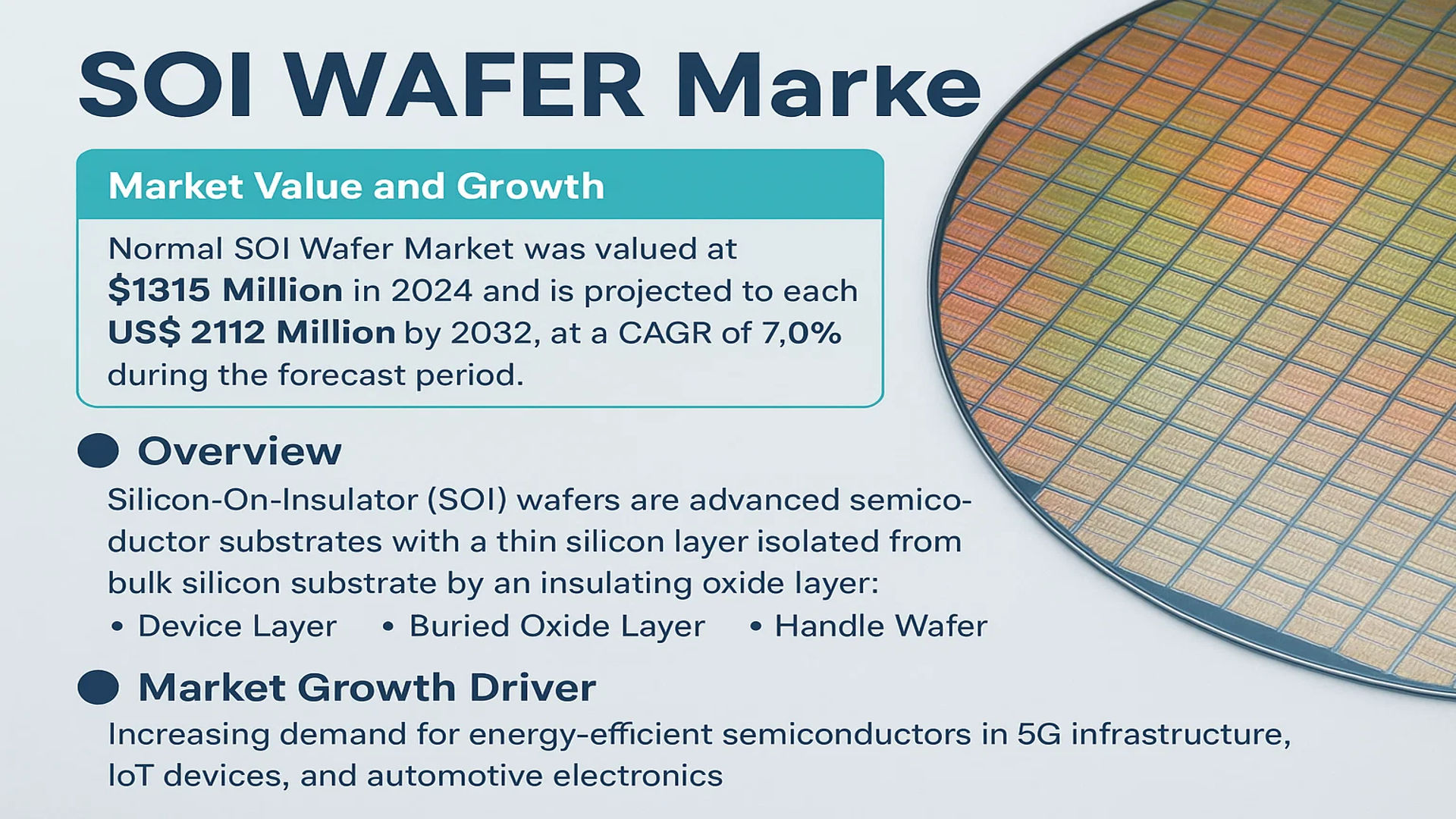
The global Normal SOI Wafer Market was valued at 1315 million in 2024 and is projected to reach US$ 2112 million by 2032, at a CAGR of 7.0% during the forecast period.
Silicon-On-Insulator (SOI) wafers are advanced semiconductor substrates where a thin silicon layer is isolated from the bulk silicon substrate by an insulating oxide layer. This unique structure enhances performance in applications requiring low power consumption, reduced leakage currents, and improved radiation hardness compared to traditional bulk silicon wafers. The key layers include the device layer (for transistor fabrication), buried oxide layer (for electrical isolation), and handle wafer (for mechanical support).
Market growth is driven by increasing demand for energy-efficient semiconductors in 5G infrastructure, IoT devices, and automotive electronics. The 300mm wafer segment dominates due to high-volume manufacturing needs, while RF applications are growing rapidly with 5G deployment. Key players like Soitec and Shin-Etsu control over 60% of the market, with strategic expansions in Asia-Pacific to meet regional demand.
MARKET DYNAMICS
MARKET DRIVERS
Advancements in Semiconductor Technologies Accelerating SOI Wafer Adoption
The global semiconductor industry’s rapid evolution is a key driver for the SOI wafer market. With increasing demand for high-performance, energy-efficient chips across applications like 5G, IoT, and AI, SOI technology offers significant advantages over traditional bulk silicon. Its superior performance in reducing power consumption while maintaining high speed makes it ideal for modern electronics. The growing adoption of 300mm SOI wafers in foundries worldwide reflects this trend, with production volumes increasing by approximately 18% annually since 2021. Leading semiconductor companies are increasingly integrating SOI solutions into their advanced node manufacturing processes.
5G Infrastructure Deployment Fueling RF-SOI Demand
The global rollout of 5G networks presents a major growth opportunity for RF-SOI wafers, which are essential components in 5G front-end modules. With over 2 million 5G base stations expected to be deployed worldwide by 2025, the demand for high-frequency, low-loss SOI substrates continues to rise. RF-SOI offers superior linearity and isolation characteristics crucial for 5G antennas and power amplifiers. Major foundries have reported RF-SOI wafer shipments growing at a compound annual rate of 12-15% to meet this demand, with particular strength in millimeter-wave applications.
Automotive Semiconductor Boom Driving SOI Market Expansion
The automotive industry’s digital transformation is creating substantial demand for SOI wafers, particularly in electric vehicle power management and advanced driver assistance systems (ADAS). SOI technology’s ability to withstand high temperatures and voltages makes it ideal for automotive applications. With the global automotive semiconductor market projected to reach $100 billion by 2026, SOI wafer manufacturers are seeing growing orders from Tier 1 suppliers. Power-SOI solutions, in particular, are experiencing strong adoption for battery management systems in EVs, with some manufacturers reporting 25-30% annual growth in this segment.
MARKET RESTRAINTS
High Production Costs Limiting Market Penetration
While SOI technology offers numerous advantages, its higher production costs compared to conventional silicon remain a significant barrier to broader adoption. The specialized manufacturing processes required for SOI wafers can increase substrate costs by 2-3 times versus bulk silicon. This cost premium is particularly challenging in price-sensitive consumer electronics markets, where manufacturers must carefully balance performance benefits against bill-of-materials considerations. Some semiconductor companies hesitate to transition designs to SOI due to these economic factors, despite the technology’s technical merits.
Complex Manufacturing Processes Creating Supply Challenges
The SOI wafer production process involves sophisticated technologies like ion implantation and wafer bonding, requiring substantial capital investment and specialized expertise. Establishing new production capacity can take 18-24 months, creating challenges in responding to sudden demand spikes. Recent industry reports indicate that lead times for certain SOI wafer types have extended to 6-9 months amid strong demand, potentially hampering market growth. Furthermore, the complexity of SOI manufacturing results in lower yields compared to bulk silicon, particularly for advanced node applications.
MARKET CHALLENGES
Intense Competition from Alternative Semiconductor Materials
The SOI wafer market faces increasing competition from emerging semiconductor materials like silicon carbide (SiC) and gallium nitride (GaN), particularly in power electronics applications. While SOI offers advantages in certain use cases, these alternative materials provide superior performance in high-power, high-temperature environments. The power semiconductor market’s rapid adoption of wide-bandgap materials presents a competitive challenge for SOI technology, requiring continuous innovation to maintain market share. Some industry analysts project that SiC and GaN could capture 30-40% of the power device market by 2030, potentially limiting SOI’s growth potential in this segment.
Other Challenges
Design Complexity and Ecosystem Development
Transitioning to SOI-based designs requires specialized expertise and IP development, creating barriers for smaller semiconductor companies. While the ecosystem for bulk silicon design tools and IP is well-established, SOI-specific resources remain more limited. This design complexity can increase development costs and time-to-market for new SOI-based products, particularly in application areas where the technology is still maturing.
MARKET OPPORTUNITIES
Emerging Photonics Applications Creating New Growth Avenues
The growing photonics market presents significant opportunities for SOI wafer manufacturers, particularly in data center and telecommunications applications. Silicon photonics leverages SOI substrates to integrate optical components with electronic circuits, enabling high-speed data transmission with lower power consumption. With hyperscale data centers increasingly adopting co-packaged optics solutions, the demand for photonics-enabled SOI wafers is expected to grow at over 20% annually through 2030. Several leading foundries have recently expanded their SOI photonics capabilities to capitalize on this trend.
Advanced Packaging Technologies Opening New Applications
The semiconductor industry’s shift toward advanced packaging architectures like 3D ICs and chiplets creates new opportunities for SOI technology. SOI wafers’ excellent thermal and electrical isolation properties make them attractive for heterogeneous integration applications. Manufacturers are developing specialized SOI solutions for 2.5D and 3D packaging, particularly in high-performance computing and AI accelerator markets. These emerging applications could drive significant growth for the SOI market beyond traditional front-end semiconductor manufacturing.
NORMAL SOI WAFER MARKET TRENDS
Strong Adoption in 5G and IoT Applications Drives Market Expansion
The growing deployment of 5G networks and Internet of Things (IoT) devices is significantly boosting the demand for Silicon-On-Insulator (SOI) wafers. These wafers play a critical role in advanced semiconductor applications where low power consumption and high-frequency performance are essential. RF SOI wafers, in particular, are increasingly being used in 5G infrastructure due to their superior signal integrity and reduced energy loss. Additionally, the miniaturization trend in consumer electronics and edge computing devices has further accelerated the adoption of SOI-based components. While the transition to higher wafer sizes (such as 300mm) is gaining traction, manufacturers continue to optimize existing technologies to enhance production efficiency.
Other Trends
Automotive and Power Electronics Demand Surge
The automotive industry’s shift towards electric vehicles (EVs) and advanced driver-assistance systems (ADAS) is fueling the need for SOI wafers in power semiconductor devices. These wafers offer better thermal management and higher reliability compared to traditional bulk silicon, making them ideal for high-voltage applications in EVs. Moreover, the increasing adoption of wide-bandgap semiconductors (such as SiC and GaN) is complementing the growth of SOI wafers in the power sector, as they enhance switching efficiency and reduce energy losses. Regional mandates for energy-efficient electronics are also pushing manufacturers to invest in SOI-based solutions.
Rising Investments in Semiconductor Manufacturing
The global semiconductor industry is witnessing record investments in fabrication facilities (fabs), particularly in regions like North America and Asia-Pacific. Governments worldwide are actively supporting domestic semiconductor production to reduce reliance on imports, leading to new SOI wafer production plants. Meanwhile, manufacturers are scaling up 200mm and 300mm wafer production to meet the rising demand from integrated device manufacturers (IDMs). Innovations in bonding techniques and defect reduction in SOI fabrication are also enhancing yield rates, ensuring cost-effective production. While supply chain disruptions remain a challenge, strategic collaborations between foundries and material suppliers are stabilizing raw material availability.
COMPETITIVE LANDSCAPE
Key Industry Players
Semiconductor Giants Innovate to Capitalize on the Expanding SOI Market
The global Normal SOI Wafer market is characterized by intense competition, with leading semiconductor manufacturers and specialized wafer producers vying for market dominance. Soitec, a French semiconductor materials company, currently leads the market with its proprietary Smart Cut™ technology, which enables high-volume production of superior quality SOI wafers. The company’s strong presence in Europe, North America, and Asia positions it as a key supplier for major foundries and IDMs.
Another significant player, Shin-Etsu Chemical, leverages its vertical integration in silicon production to offer competitively priced SOI wafers, particularly in the Japanese and Asian markets. Meanwhile, SUMCO Corporation and GlobalWafers are strengthening their positions through capacity expansions and technological partnerships. These companies are actively developing advanced 300mm SOI wafers to meet the growing demand from high-performance computing and 5G RF applications.
The competitive intensity is further amplified by regional specialists like China’s Shanghai Advanced Silicon Technology and Shenyang Silicon Technology, which are rapidly gaining traction in domestic markets through government-supported semiconductor initiatives. These manufacturers are focusing on improving yield rates and reducing production costs to compete with established international players.
Investment in R&D remains a critical differentiator, with companies like IceMos Technology developing specialized SOI solutions for niche applications such as power electronics and MEMS. While the market shows consolidation trends among top players, smaller specialized manufacturers continue to thrive in specific applications where customized SOI solutions are required.
List of Key Normal SOI Wafer Manufacturers
- Soitec (France)
- Shin-Etsu Chemical Co., Ltd. (Japan)
- SUMCO Corporation (Japan)
- GlobalWafers Co., Ltd. (Taiwan)
- NSIG (Okmetic) (Finland)
- IceMos Technology (U.K.)
- Wafer Works Corporation (Taiwan)
- Shenyang Silicon Technology (China)
- Zhonghuan Advanced Semiconductor Materials (China)
- Shanghai Advanced Silicon Technology (China)
- WaferPro (U.S.)
- SEIREN KST (Japan)
- PlutoSemi (China)
Segment Analysis:
By Type
300 mm Segment Leads Due to High Demand in Advanced Semiconductor Manufacturing
The market is segmented based on wafer size into:
- 150mm and Below
- 200mm
- 300mm
By Application
RF Devices Segment Dominates with Increasing 5G and IoT Adoption
The market is segmented based on application into:
- Power Devices
- MEMS
- RF Devices
- Optoelectronic Devices
- Others
By End User
Consumer Electronics Industry Accounts for Largest Adoption
The market is segmented based on end user into:
- Consumer Electronics
- Automotive
- Telecommunications
- Industrial
- Others
By Technology
Smart Cut Technology Preferred for Superior Performance Characteristics
The market is segmented based on manufacturing technology into:
- Smart Cut
- Bonded SOI
- SIMOX
- Others
Regional Analysis: Normal SOI Wafer Market
Asia-Pacific
The Asia-Pacific region dominates the global Normal SOI Wafer market, accounting for the highest revenue share due to strong semiconductor manufacturing ecosystems in China, Japan, and South Korea. With China’s rapid adoption of SOI wafers in 5G infrastructure and IoT applications, the country leads regional growth. Japan remains a technological hub, leveraging SOI wafers for advanced automotive and industrial semiconductors. While cost sensitivity still favors conventional wafers in some areas, government initiatives like China’s 14th Five-Year Plan are accelerating the transition to SOI-based solutions. Key challenges include supply chain dependencies and shifting trade policies affecting wafer imports.
North America
North America’s SOI wafer demand is driven by high-performance computing (HPC), aerospace, and defense applications, where the low-power advantages of SOI technology are critical. The U.S. holds the largest market share in the region, supported by investments in AI infrastructure and partnerships between semiconductor firms like GlobalWafers and research institutions. While environmental regulations are less stringent compared to Europe, emphasis on energy-efficient chips is growing. However, reliance on Asian suppliers for raw materials creates vulnerability, prompting initiatives to strengthen domestic manufacturing capabilities under the CHIPS and Science Act.
Europe
Europe focuses on MEMS and RF applications for automotive and industrial automation, with strict environmental standards promoting SOI wafer adoption. France’s Soitec leads innovation through partnerships with STMicroelectronics. The EU’s Horizon Europe program funds R&D in semiconductor materials, but higher production costs compared to Asia remain a barrier. Recent geopolitical tensions have exposed supply chain risks, prompting efforts to localize production. Germany and the Benelux countries are key markets, though growth is slower due to competition from cheaper bulk silicon alternatives in cost-sensitive segments.
South America
South America’s SOI wafer market is nascent, with Brazil showing early adoption in medical devices and renewable energy systems. Limited local manufacturing forces reliance on imports, primarily from Asia and North America. Economic instability and underdeveloped semiconductor ecosystems hinder large-scale adoption. Nevertheless, pilot projects in Argentina and Chile indicate potential, particularly for MEMS sensors in agriculture and mining. Infrastructure gaps and low R&D investment delay widespread commercialization, though gradual industrialization offers long-term opportunities.
Middle East & Africa
The MEA region is emerging as a niche market, with Israel and the UAE leading in aerospace and telecommunications applications. Local production is minimal, but partnerships with global players like Tower Semiconductor (Israel) signal growing interest. High costs and limited technical expertise slow adoption, though sovereign wealth funds in GCC countries are investing in technology hubs to diversify economies beyond oil. Africa’s market remains untapped except for South Africa’s medical and automotive sectors, where SOI wafers are imported for specialized applications.
Report Scope
This market research report provides a comprehensive analysis of the global Normal SOI Wafer market, covering the forecast period 2025–2032. It offers detailed insights into market dynamics, technological advancements, competitive landscape, and key trends shaping the semiconductor substrate industry.
Key focus areas of the report include:
- Market Size & Forecast: Historical data and future projections for revenue, unit shipments, and market value across major regions and segments. The global Normal SOI Wafer market was valued at USD 1,315 million in 2024 and is projected to reach USD 2,112 million by 2032, growing at a CAGR of 7.0%.
- Segmentation Analysis: Detailed breakdown by wafer size (150mm and Below, 200mm, 300mm) and application (Power Devices, MEMS, RF Devices, Optoelectronic Devices, Others) to identify high-growth segments.
- Regional Outlook: Insights into market performance across North America, Europe, Asia-Pacific, Latin America, and Middle East & Africa. Asia-Pacific dominates with major contributions from China, Japan and South Korea.
- Competitive Landscape: Profiles of leading manufacturers including Soitec, Shin-Etsu, SUMCO, GlobalWafers and NSIG (Okmetic), covering their product portfolios, market shares, and strategic developments.
- Technology Trends & Innovation: Assessment of SOI wafer fabrication techniques, emerging applications in 5G and IoT devices, and advancements in semiconductor manufacturing processes.
- Market Drivers & Restraints: Analysis of factors such as growing demand for high-performance semiconductors, while addressing challenges like high manufacturing costs and complex fabrication processes.
- Stakeholder Analysis: Strategic insights for semiconductor manufacturers, foundries, equipment suppliers, and investors regarding market opportunities and competitive positioning.
The research employs both primary and secondary methodologies, including interviews with industry experts and analysis of verified market data, to ensure accuracy and reliability of findings.
FREQUENTLY ASKED QUESTIONS:
What is the current market size of Global Normal SOI Wafer Market?
-> Normal SOI Wafer Market was valued at 1315 million in 2024 and is projected to reach US$ 2112 million by 2032, at a CAGR of 7.0% during the forecast period.
Which key companies operate in Global Normal SOI Wafer Market?
-> Key players include Soitec, Shin-Etsu, SUMCO, GlobalWafers, NSIG (Okmetic), IceMos Technology, and Wafer Works Corporation, among others.
What are the key growth drivers?
-> Primary growth drivers include increasing demand for high-performance semiconductors, expansion of 5G networks, and growing adoption in IoT devices.
Which region dominates the market?
-> Asia-Pacific leads the market, accounting for over 45% of global demand, driven by semiconductor manufacturing in China, Japan and South Korea.
What are the emerging trends?
-> Emerging trends include advancements in wafer bonding techniques, development of ultra-thin SOI wafers, and increasing adoption in automotive electronics.

Get Sample Report PDF for Exclusive Insights
Report Sample Includes
- Table of Contents
- List of Tables & Figures
- Charts, Research Methodology, and more...
 Download Sample Report PDF







