LED Epitaxial Wafer Market Insights
LED Epitaxial Wafer market is projected to grow from USD 1,141 million in 2026 to USD 2,029 million by 2034, exhibiting a CAGR of 8.7% during the forecast period.
LED epitaxial wafers are core semiconductor material products positioned upstream in the LED value chain. In essence, they are bare epitaxial wafers on which multilayer light‑emitting structures are grown on substrates such as sapphire, GaAs, GaP, silicon or GaN via MOCVD or LPE processes before being supplied to downstream chip makers for photolithography and metallisation.
The market is gaining momentum because manufacturers are expanding customized growth services for visible‑light, UV, IR and Mini‑/Micro‑LED applications. Key players such as Resonac Corporation, Nichia Corporation and Ennostar Corporation are investing in larger‑diameter wafer platforms and defect‑density reduction technologies to meet automotive lighting and high‑resolution display demands.
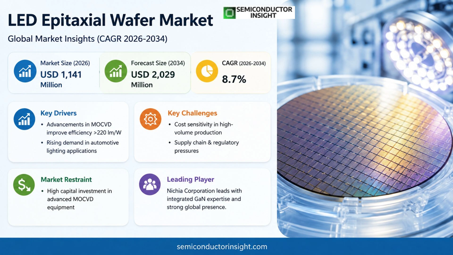
MARKET DRIVERS
Technological Advancements in Substrate Engineering
Recent breakthroughs in metal‑organic chemical vapor deposition (MOCVD) have sharpened thickness uniformity to below 1 µm, allowing manufacturers to push luminous efficacy beyond 220 lm/W. This level of precision reduces reject rates, making large‑area wafers financially viable for premium automotive and horticultural lighting applications. As a result, producers are expanding capacity to capture the incremental value created by higher‑efficiency devices.
Growing Adoption in Automotive Lighting
The shift toward OLED‑free tail‑lights and matrix‑LED headlamps is compelling automakers to source wafers with tighter spectral control. In 2023, automotive‑grade LED epitaxial wafers accounted for roughly 30 % of total shipments, up from 22 % the previous year, indicating that vehicle manufacturers are willing to pay a premium for performance‑optimized substrates. This trend feeds directly into higher‑margin orders for wafer suppliers.
➤ Industry insiders note that the convergence of higher driving currents and advanced chip‑on‑wafer designs is redefining the cost structure of LED Epitaxial Wafer Market.
In parallel, the data‑center lighting segment is embracing high‑density LED arrays that demand wafers with minimal defect density. Suppliers that can guarantee sub‑10‑ppm dislocation levels are gaining preferential placement in multi‑year contracts, reinforcing the upward trajectory of demand across multiple end‑markets.
MARKET CHALLENGES
Cost Sensitivity in High‑Volume Production
While yield improvements have narrowed the gap between premium and commodity wafers, the price differential remains a decisive factor for volume manufacturers. A 5 % increase in wafer price can erode the profitability of large‑scale LED modules, prompting buyers to renegotiate pricing or explore alternative material sources such as sapphire substrates that offer lower entry costs.
Other Challenges
Supply Chain Volatility
The reliance on specialty gases and ultra‑pure silicon precursors creates exposure to geopolitical disruptions. Recent logistics bottlenecks in East Asia have extended lead times by up to 45 days, forcing end‑users to hold higher inventory buffers and consequently tightening cash flow.
Regulatory Hurdles
Stringent environmental regulations governing the use of certain phosphors and the disposal of hazardous by‑products are tightening in major markets. Compliance costs are rising, and firms that lack robust waste‑management protocols risk penalties that can offset gains from higher wafer performance.
MARKET RESTRAINTS
Capital Intensity of Advanced Deposition Equipment
State‑of‑the‑art MOCVD reactors exceed $30 million in capital outlay, a barrier that limits new entrants and concentrates production within a handful of global players. The long amortization periods compel existing manufacturers to adopt conservative capacity‑expansion strategies, dampening rapid scale‑up.
Financing constraints become more pronounced when macroeconomic conditions tighten, as lenders scrutinize the long‑term return profile of wafer production lines that typically require 3‑5 years to achieve break‑even.
Furthermore, the necessity for clean‑room environments that meet Class 100 standards adds operational overhead, increasing per‑wafer cost and restricting price flexibility in price‑sensitive segments.
MARKET OPPORTUNITIES
Expansion into Smart‑City Lighting Infrastructure
Municipal initiatives to retrofit streetlights with adaptive LED systems are projected to generate a sizable demand surge for high‑performance wafers. Cities are budgeting for installations that integrate sensors and IoT connectivity, necessitating substrates that sustain higher current densities while maintaining color stability. Suppliers that align product roadmaps with these specifications can capture a share of the multi‑billion‑dollar smart‑city lighting spend.
Another avenue lies in the miniaturization of wearable health‑monitoring devices, where ultra‑thin, flexible LED arrays require epitaxial wafers fabricated on novel carrier materials. Early‑stage collaborations between wafer fabs and flexible‑electronics firms are already yielding prototype modules, pointing to a nascent but high‑margin niche.
Finally, the emergence of vertical farming as a commercial agricultural model is spurring demand for full‑spectrum LEDs tuned to specific plant growth cycles. Wafer manufacturers that can tailor bandgap engineering to produce precise photon outputs will find a receptive market willing to pay premiums for yield‑enhancing lighting solutions.
LED Epitaxial Wafer Market Trends
Shift Toward High‑Value Display and Automotive Segments
LED Epitaxial Wafer Market recorded revenue of roughly US$1.14 billion in 2025. Forecasts indicate the market will reach about US$2.03 billion by 2034, reflecting an average annual increase near 8.7 percent. This expansion is not rooted in conventional lighting alone; instead, manufacturers are channeling capacity into Mini‑LED, Micro‑LED, and automotive headlamp applications that demand larger wafers, tighter uniformity, and custom wavelength stacks. The higher device efficiency and miniaturization trends in consumer electronics and vehicle illumination raise the bar for epitaxial quality, prompting buyers to seek suppliers that can deliver defect‑free, high‑yield substrates. As a result, pricing pressure eases for commoditized sizes while premium‑grade wafers command stronger margins.
Other Trends
Supply‑Side Consolidation and Integrated Services
Leading producers have broadened their portfolios beyond bare wafers to include foundry‑type services that merge epitaxial growth with downstream chip processing. Companies in Japan, South Korea, and mainland China now operate multi‑platform lines covering GaAs, GaP, and GaN, and they are investing heavily in MOCVD and LPE tool upgrades. This vertical integration reduces hand‑off loss, improves yield predictability, and creates a sticky customer base. The competitive arena has migrated from a sole focus on brightness to a suite of attributes,wafer size, defect density, and compatibility with downstream photolithography. Firms that can co‑develop custom layer structures while offering volume manufacturing are gaining pricing power and reinforcing market concentration around a handful of technologically mature players.
Demand Diversification Across Industries
Beyond display panels, emerging uses such as ultraviolet disinfection, infrared sensing for automotive safety, and short‑wave infrared (SWIR) communications are reshaping the order book for epitaxial wafers. Policy incentives in China, Europe, and the United States encouraging energy‑efficient lighting and advanced optics amplify this effect. Consequently, the geographic spread of end‑use demand now mirrors a more balanced global footprint, with strong pull from North America and Europe for high‑reliability chips, while Asian manufacturers satisfy mass‑market volume needs. The combined impact of these application pulls is a market that grows at a measured pace overall but exhibits accelerated momentum in high‑margin niches, compelling suppliers to prioritize R&D investments that address wavelength precision and large‑area uniformity.
COMPETITIVE LANDSCAPE
Key Industry Players
Competitive dynamics shaping LED Epitaxial Wafer sector
Nichia Corporation commands the largest share of LED Epitaxial Wafer market, leveraging its deep GaN expertise and a vertically integrated production line that spans sapphire‑based substrates to monolithic RGB devices. By offering a portfolio that covers visible, UV and IR wavelengths, Nichia can satisfy the divergent needs of automotive lighting, high‑brightness display backlights, and emerging micro‑LED panels. Its ability to combine low defect density with wafer sizes up to 6‑inch gives downstream chip makers a reliable foundation for high‑volume manufacturing, reinforcing Nichia’s pricing leverage and cementing long‑term customer relationships.
Beyond the dominant players, several niche firms are gaining traction by targeting specialized wavelength bands or advanced process architectures. Resonac (formerly Sony) excels in high‑performance GaAs and GaP platforms for infrared sensing, while Nitride Semiconductors Co., Ltd. focuses on ultra‑high‑efficiency UV epitaxial layers for sterilization equipment. Korean outfits such as Ennostar Corporation and PROWTech differentiate themselves through template‑based epitaxy that enables rapid scaling to 8‑inch wafers for micro‑LED displays. European entrants like Soft‑EPi and the UK‑based BOE HC Semitek are building foundry services around mini‑LED and micro‑LED monolithic RGB growth, attracting premium customers seeking co‑development. Chinese manufacturers,including Xiamen Changelight, Sanan Optoelectronics and SensLite,provide a breadth of size options and price points, capitalising on domestic demand for automotive lighting and consumer electronics. The overall structure resembles an oligopoly at the high‑end (large‑wafer, low‑defect GaN) and a fragmented field of specialized suppliers serving emerging applications.
List of Key LED Epitaxial Wafer Companies Profiled
- Nichia Corporation
- Resonac Corporation
- Nitride Semiconductors Co., Ltd.
- Ennostar Corporation
- PROWTech
- Soft‑EPi
- BOE HC Semitek Corporation
- Xiamen Changelight Co., Ltd.
- Sanan Optoelectronics Co., Ltd.
- SensLite Corporation
- Seoul Semiconductor Co., Ltd.
- Cree, Inc. (Wolfspeed)
- Sumitomo Osaka Cement Co., Ltd.
- Signify (Philips Lighting)
- Hikvision Electronics (Epitaxy Division)
Segment Analysis:
| Segment Category | Sub-Segments | Key Insights |
| By Type |
|
GaN‑Based Wafer is the dominant type driving broad application reach. – Suppliers emphasize low defect density and high uniformity to support advanced displays. – Integration with downstream chip processes is a decisive factor for customer loyalty. – Continuous R&D on substrate compatibility expands design flexibility. |
| By Application |
|
Micro LED Displays emerge as the most demanding application. – Requires exceptionally high wafer uniformity across large diameters. – Emphasis on red efficiency and monolithic RGB structures. – Foundry‑style services create strategic partnerships with display manufacturers. |
| By End User |
|
Display and Backlight Providers drive the highest value chain engagement. – Seek customized epitaxial structures to achieve superior color rendering. – Prioritize wafer suppliers that can co‑develop and offer integrated foundry services. – Long‑term contracts are built around reliability and yield consistency. |
| By Emission Band |
|
Visible Light Wafer remains the core driver for mainstream lighting and display markets. – Offers the broadest substrate compatibility and established supply chains. – Continuous improvements in luminous efficiency and thermal management are focal points. – Enables smooth transition to higher‑performance display formats. |
| By Growth Technique |
|
MOCVD Platform is recognized as the technological backbone for high‑performance wafers. – Delivers precise compositional control essential for multi‑color emission. – Supports scaling to larger wafer diameters demanded by advanced displays. – Ongoing equipment upgrades reinforce yield and reliability advantages. |
Regional Analysis: LED Epitaxial Wafer Market
Asia‑Pacific
Recent plant start‑ups in China, Taiwan, and South Korea have lifted regional throughput, allowing suppliers to meet the rising demand for high‑brightness LEDs used in automotive lighting. Capacity additions are paired with incremental automation, which drives per‑wafer cost efficiencies without compromising wafer integrity.
The region’s proximity to critical raw‑material sources, such as high‑purity gallium and indium, reduces exposure to logistics bottlenecks. Vertically integrated players mitigate disruption risk by controlling substrate preparation, epitaxial growth, and downstream polishing within a single corporate structure.
Incentive frameworks that target green‑technology manufacturing reward investments in energy‑efficient LED solutions. Subsidies for research in novel quantum‑well designs encourage collaboration between academia and industry, accelerating the arrival of next‑generation wafer architectures.
Tier‑1 display manufacturers dominate the demand curve, yet a rising cohort of automotive OEMs seeks customized epitaxial stacks for vehicle lighting. This diversification forces wafer providers to adopt flexible production schedules and develop application‑specific quality metrics.
North America
In North America, LED Epitaxial Wafer market is shaped by a concentration of high‑end R&D hubs and a customer base that prizes reliability above all. End‑users such as aerospace lighting contractors demand stringent defect‑density tolerances, prompting wafer producers to embed advanced inspection tools within their lines. While overall volume lags behind Asia‑Pacific, pricing power remains strong, as buyers are willing to pay premiums for traceability and compliance with rigorous safety standards. Strategic alliances between U.S. fabless firms and Asian manufacturers are common, allowing North American designers to tap into cost‑effective supply while retaining control over specifications.
Europe
European activity in LED Epitaxial Wafer arena reflects a balance between sustainability mandates and a mature automotive sector. Regulations that limit light‑pollution and encourage energy‑saving illumination have spurred investment in high‑efficiency wafer processes, particularly in Germany and France. At the same time, the continent’s push toward electric‑vehicle adoption creates a steady flow of orders for specialized wafer geometries. Companies operating in Europe frequently differentiate themselves through advanced metrology services, catering to OEMs that require tight process windows and consistent performance across multiple production cycles.
South America
South America presents a nascent but steadily growing market for LED epitaxial wafers, driven largely by expanding residential lighting projects and government‑backed energy‑efficiency programs. Brazil and Mexico lead procurement activities, often sourcing wafers from established Asian suppliers while establishing local assembly capabilities. The region’s cost‑sensitivity forces vendors to offer tiered pricing structures, and many are experimenting with bundled services that include wafer handling and basic packaging to reduce total ownership cost for end‑users.
Middle East & Africa
The Middle East & Africa segment remains underpenetrated, yet recent large‑scale infrastructure initiatives,especially smart‑city developments in the United Arab Emirates and renewable‑energy installations in South Africa,are creating pockets of demand for high‑brightness LED solutions. Procurement strategies here lean on long‑term supply contracts, with buyers seeking reliability and after‑sales technical support to mitigate the scarcity of local technical expertise. Suppliers that can provide comprehensive training and remote diagnostic tools are gaining a foothold, positioning themselves for future growth as regional policies increasingly endorse energy‑saving lighting standards.
Report Scope
This market research report provides a comprehensive analysis of the LED Epitaxial Wafer Market , covering the forecast period 2026–2034. It offers detailed insights into market dynamics, technological advancements, competitive landscape, and key trends shaping the industry.
Key focus areas of the report include:
- Market Overview: The report begins with an overview outlining its current market scenario, key growth indicators, and industry transformation drivers. It discusses macroeconomic factors, demand–supply balance, regulatory landscape, and the strategic role of semiconductors in powering advancements across industries such as automotive, telecommunications, consumer electronics, and industrial automation.
- Market Size & Forecast: Historical data and future projections for revenue, unit shipments, and market value across major regions and segments.
- Segmentation Analysis: Detailed breakdown by product type, technology, application, and end-user industry to identify high-growth segments and investment opportunities.
- Regional Insights: Insights into market performance across North America, Europe, Asia-Pacific, Latin America, and the Middle East & Africa, include country‑level analysis where relevant.
- Competitive Landscape: Profiles of leading market participants, including their product offerings, R&D focus, manufacturing capacity, pricing strategies, and recent developments such as mergers, acquisitions, and partnerships.
- Technology Trends & Innovation: Assessment of emerging technologies, integration of AI/IoT, semiconductor design trends, fabrication techniques, and evolving industry standards.
- Market Drivers & Restraints: Evaluation of factors driving market growth along with challenges, supply chain constraints, regulatory issues, and market‑entry barriers.
- Stakeholder Insights: Insights for component suppliers, OEMs, system integrators, investors, and policymakers regarding the evolving ecosystem and strategic opportunities.
Primary and secondary research methods are employed, including interviews with industry experts, data from verified sources, and real‑time market intelligence to ensure the accuracy and reliability of the insights presented.
FREQUENTLY ASKED QUESTIONS:
What is the current market size of LED Epitaxial Wafer Market?
-> LED Epitaxial Wafer market is projected to grow from USD 1,141 million in 2026 to USD 2,029 million by 2034, exhibiting a CAGR of 8.7%
Which key companies operate in LED Epitaxial Wafer Market?
-> Key players include Resonac Corporation, Nichia Corporation, Nitride Semiconductors Co., Ltd., Ennostar Corporation, PROWTech, Soft-EPi, BOE HC Semitek Corporation, Xiamen Changelight Co., Ltd., Sanan Optoelectronics Co., Ltd., and SensLite Corporation.
What are the key growth drivers?
-> Key growth drivers include increasing adoption of Micro LED and Mini LED displays, expansion of automotive lighting and advanced driver‑assistance systems, growth of UV disinfection and infrared sensing markets, and supportive energy‑efficiency policies in China, Europe and the United States.
Which region dominates the market?
-> Asia (East Asia) holds the largest share of production capacity and demand, with China, Japan, South Korea and Taiwan leading the market.
What are the emerging trends?
-> Emerging trends include micro‑LED display integration, monolithic RGB epitaxy, UV curing solutions, infrared & SWIR sensing platforms, and AR/VR near‑eye display applications.

Get Sample Report PDF for Exclusive Insights
Report Sample Includes
- Table of Contents
- List of Tables & Figures
- Charts, Research Methodology, and more...