MARKET INSIGHTS
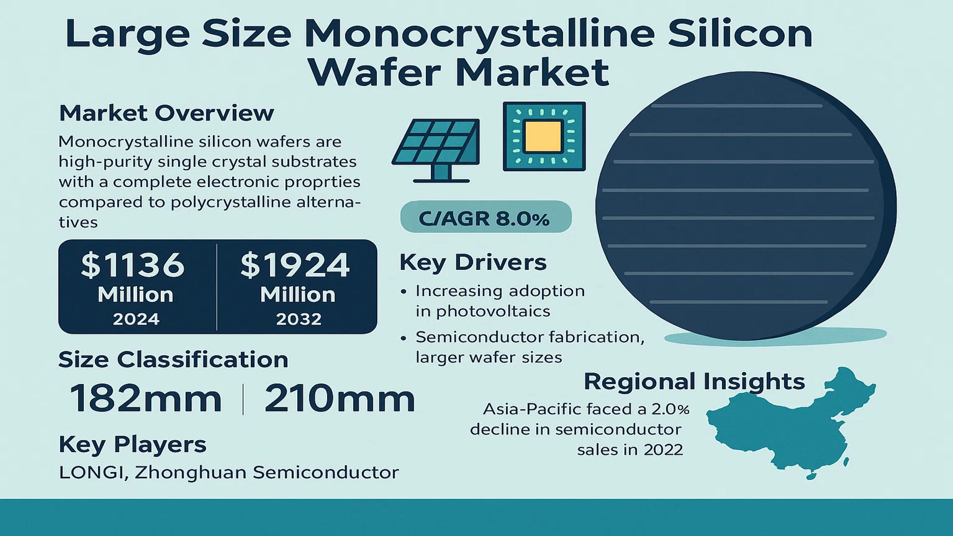
The global Large Size Monocrystalline Silicon Wafer Market was valued at 1136 million in 2024 and is projected to reach US$ 1924 million by 2032, at a CAGR of 8.0% during the forecast period. While the semiconductor industry experienced a slowdown in 2022, with global revenues growing only 4.4% to USD 580 billion, demand for advanced silicon wafers remains robust due to their critical role in electronics and solar applications.
Monocrystalline silicon wafers are high-purity single-crystal substrates with a complete lattice structure, offering superior electronic properties compared to polycrystalline alternatives. These wafers are classified by size, with 182mm and 210mm being the dominant formats in the market. Their uniform crystal orientation makes them ideal for high-efficiency solar cells and precision semiconductor devices.
The market growth is driven by increasing adoption in photovoltaics, where monocrystalline silicon achieves conversion efficiencies exceeding 22%, and semiconductor fabrication, where larger wafer sizes improve manufacturing economies of scale. However, Asia-Pacific—the largest regional market—faced a 2.0% decline in semiconductor sales in 2022, reflecting broader supply chain adjustments. Key players like LONGi and Zhonghuan Semiconductor are expanding production capacities to meet demand, with the 210mm wafer segment gaining traction for next-generation solar modules.
MARKET DYNAMICS
MARKET DRIVERS
Rising Demand for High-Efficiency Solar Panels Accelerates Market Growth
The global shift towards renewable energy sources has significantly increased demand for large size monocrystalline silicon wafers, which form the backbone of high-efficiency solar panels. Monocrystalline silicon wafers offer superior efficiency (typically 20-25%) compared to polycrystalline alternatives, making them the material of choice for premium solar applications. The photovoltaic industry accounted for over 65% of total wafer demand in 2024, with projections indicating this share will grow to nearly 72% by 2030. Recent technological advancements have further enhanced wafer performance, with leading manufacturers achieving conversion efficiencies above 24% in mass production settings.
Semiconductor Industry Expansion Creates Sustained Demand
The relentless growth of the semiconductor industry continues to drive wafer market expansion. Large diameter wafers (200mm and above) are becoming increasingly critical for advanced semiconductor manufacturing, particularly for memory chips and power devices. The global semiconductor market, valued at approximately $580 billion in 2022, maintains stable wafer demand despite cyclical fluctuations. Emerging technologies such as 5G, AI chips, and IoT devices all rely on high-quality monocrystalline silicon substrates, ensuring long-term market sustainability. The transition to larger wafer sizes (210mm versus traditional 182mm) further boosts material requirements per unit.
Government Clean Energy Policies Stimulate Market Growth
Global decarbonization initiatives are providing strong policy support for monocrystalline silicon wafer manufacturers. The European Union’s REPowerEU plan aims to install over 600 GW of solar capacity by 2030, while similar programs in the U.S. (Inflation Reduction Act) and China are driving unprecedented solar deployment. These policies typically include local content requirements that benefit domestic wafer producers. International collaboration on renewable energy targets has created a robust policy environment that assures long-term market stability and attracts billions in manufacturing investments.
MARKET RESTRAINTS
High Manufacturing Costs Challenge Market Penetration
While monocrystalline silicon wafers offer superior performance, their production involves sophisticated and capital-intensive processes. The Czochralski growth method, used for producing single-crystal ingots, requires precise temperature control and high-purity polysilicon feedstock. Energy consumption accounts for approximately 30-40% of total production costs, making wafer manufacturers particularly vulnerable to electricity price fluctuations. These cost factors create barriers for new market entrants and limit adoption in price-sensitive applications, despite the technology’s performance advantages.
Complex Supply Chain Dynamics Create Volatility
The wafer manufacturing ecosystem relies on highly specialized equipment and materials from concentrated supply sources. Over 75% of polysilicon production capacity resides in China, creating potential supply bottlenecks. Trade policies and export controls in key manufacturing regions have introduced unpredictability in raw material availability. Furthermore, the semiconductor industry’s “silicon cycle” creates alternating periods of shortage and oversupply, challenging wafer producers to maintain stable operations. These supply chain complexities force manufacturers to maintain high inventory levels, tying up working capital.
MARKET CHALLENGES
Technical Limitations in Wafer Size Transition
The industry transition to larger wafer sizes (210mm) presents significant technical challenges that could delay market adoption. Increasing wafer diameter requires complete redesign of production processes, from crystal growth to slicing and polishing. Thin wafer handling becomes more difficult as sizes increase, with breakage rates potentially rising by 15-20% during the learning phase. Equipment compatibility issues affect downstream manufacturers who must retrofit entire production lines. These technical hurdles slow industry-wide adoption and require substantial capital investment from both wafer producers and their customers.
Other Challenges
Quality Consistency
Maintaining defect-free crystal structure across larger wafers demands tighter process controls. Even minor variations in oxygen content or crystal orientation can impact downstream device performance.
Environmental Regulations
Stricter controls on chemical handling and wastewater treatment increase compliance costs. The wafer manufacturing process utilizes several hazardous chemicals requiring specialized disposal protocols.
MARKET OPPORTUNITIES
Emerging Applications in Power Electronics Create New Markets
The rapid electrification of transportation and industrial systems is creating robust demand for power electronics applications. Monocrystalline silicon wafers are increasingly used in high-power IGBTs and MOSFETs for electric vehicles and renewable energy systems. The electric vehicle market alone is projected to require 35% more power semiconductors by 2030. Advanced wafer designs featuring specialized dopant profiles and crystal orientations are enabling breakthrough performance in these applications, opening new high-value market segments beyond traditional solar and semiconductor uses.
Vertical Integration Strategies Enhance Profitability
Leading manufacturers are capitalizing on opportunities to expand along the value chain. By integrating wafer production with downstream cell manufacturing, companies can capture additional margin while ensuring quality control. Several top-tier solar manufacturers have already achieved nearly 80% vertical integration. This strategy not only improves cost competitiveness but also provides insulation against supply chain disruptions. Recent expansions in Southeast Asia and North America demonstrate how geographic diversification complements vertical integration to create resilient business models in the wafer industry.
LARGE SIZE MONOCRYSTALLINE SILICON WAFER MARKET TRENDS
Shift Towards Larger Wafer Sizes to Drive Efficiency and Cost Reduction
The semiconductor and photovoltaic industries are undergoing a significant transformation with the increasing adoption of larger wafer sizes, particularly 210mm and 182mm variants, to enhance manufacturing efficiency and reduce production costs. The global large size monocrystalline silicon wafer market is projected to grow from $1,136 million in 2024 to $1,924 million by 2032, exhibiting a CAGR of 8.0%. This shift is largely driven by solar energy companies optimizing panel efficiency, where larger wafers reduce kerf loss and improve power output per module. In semiconductor production, the transition minimizes edge loss, enhancing yield per wafer. While 182mm wafers currently dominate with over 60% market share, 210mm wafers are gaining traction due to their superior cost-per-watt advantages in photovoltaics.
Other Trends
Accelerated Demand from Photovoltaic Applications
The global push for clean energy has significantly boosted photovoltaic applications, accounting for nearly 45% of wafer demand. Countries accelerating solar installations—such as China’s target of 1,200 GW renewable capacity by 2030—are fueling demand for high-efficiency monocrystalline wafers. Innovations like TOPCon (Tunnel Oxide Passivated Contact) and heterojunction solar cells further enhance wafer utilization, with efficiency rates surpassing 24% for commercial modules. However, supply chain disruptions and polysilicon price volatility remain challenges for manufacturers balancing cost and scalability.
Semiconductor Industry Expansion and Technological Integration
Advancements in 5G, IoT, and AI are escalating the need for high-purity monocrystalline silicon wafers in semiconductor fabrication. With the automotive sector’s shift toward electric vehicles (EVs) and autonomous driving, silicon carbide (SiC) wafers are emerging as a critical segment. The semiconductor wafer market grew by 4.4% in 2022, with analog and logic chips driving demand. While Asia Pacific remains the largest consumer, regional diversification is intensifying, with Europe and North America investing in localized production to mitigate geopolitical supply risks. Collaborative R&D between wafer suppliers and foundries is also optimizing defect-free wafer yields for next-gen chips.
COMPETITIVE LANDSCAPE
Key Industry Players
Leading Manufacturers Focus on Capacity Expansion and Technological Advancements
The global large-size monocrystalline silicon wafer market features a highly competitive landscape, dominated by established manufacturers with significant production capacities and technological expertise. Longi, headquartered in China, has emerged as a market leader, commanding approximately 25% of the global monocrystalline silicon wafer production capacity in 2024. The company’s dominance stems from its continuous investments in R&D and aggressive capacity expansions across Asia.
Meanwhile, Zhonghuan Semiconductor and Jinko Solar hold significant market shares, driven by their vertically integrated business models and strong presence in both domestic Chinese and international markets. These companies have been rapidly transitioning their production lines to accommodate larger wafer sizes, particularly the 210mm format, to cater to the growing demand for high-efficiency solar panels.
The photovoltaic segment accounts for over 70% of large-size monocrystalline silicon wafer demand, creating intense competition among solar manufacturers. Canadian Solar and Trina Solar have been particularly active in securing long-term wafer supply agreements to ensure stable production, with both companies announcing capacity expansion plans exceeding 10GW annually through 2026.
Smaller regional players like Solargiga Energy and Gokin Solar are focusing on niche markets and specialized applications to differentiate themselves. However, they face increasing pressure from larger competitors who benefit from economies of scale, with production costs for leading manufacturers being 15-20% lower than smaller rivals.
List of Key Large Size Monocrystalline Silicon Wafer Companies
- Longi (China)
- Zhonghuan Semiconductor (China)
- Jinko Solar (China)
- JA Solar (China)
- Canadian Solar (Canada)
- Trina Solar (China)
- Risen Energy (China)
- GCL-Poly Energy Holdings (China)
- Solargiga Energy Holding (China)
- Gokin Solar (China)
- Vritra Technologies (India)
- JYT Corporation (China)
- Shuangliang Eco-energy (China)
Segment Analysis:
By Type
210mm Opposite Side Width Dominates Owing to Higher Efficiency and Cost-Effectiveness in Large-Scale Production
The large size monocrystalline silicon wafer market is segmented by type into:
- 182mm Opposite Side Width
- 210mm Opposite Side Width
By Application
Photovoltaic Segment Leads Due to Rising Solar Energy Adoption Globally
The market is segmented based on application into:
- Semiconductor
- Photovoltaic
- Other
By End-User
Solar Panel Manufacturers Account for Majority Demand Driven by Renewable Energy Policies
The market is segmented by end-user into:
- Solar panel manufacturers
- Semiconductor device manufacturers
- Research institutions
- Others
By Production Technology
Czochralski Process Remains Dominant Due to Superior Crystal Quality
The market is segmented by production technology into:
- Czochralski process
- Float zone process
- Others
Regional Analysis: Large Size Monocrystalline Silicon Wafer Market
Asia-Pacific
Dominating the global market with over 60% share, Asia-Pacific remains the epicenter for large-size monocrystalline silicon wafer production and consumption. China leads this growth, accounting for approximately 70% of regional demand, driven by massive solar panel manufacturing and semiconductor fabrication plants. The region benefits from well-established supply chains, governmental subsidies for renewable energy projects, and increasing investments in photovoltaic capacity expansion. Key players like LONGi and Zhonghuan Semiconductor have accelerated production of 210mm wafers to meet the booming demand from solar installers across India, Japan, and Southeast Asia. While cost competitiveness remains paramount, technology transitions toward higher efficiency PERC and TOPCon solar cells are reshaping wafer specifications across the region.
North America
The North American market prioritizes technological innovation and quality standards, with the U.S. accounting for 85% of regional wafer demand. Semiconductor applications dominate here, particularly for advanced nodes below 7nm where wafer defect rates critically impact yields. Recent CHIPS Act allocations of $52 billion for domestic semiconductor manufacturing are stimulating new fab constructions, consequently driving specialty wafer demand. While photovoltaic adoption grows steadily through utility-scale solar projects, regulatory complexities and trade tariffs on imported wafers create supply chain uncertainties. Manufacturers are increasingly collaborating with national labs to develop wafer technologies optimizing both solar conversion efficiency and semiconductor performance metrics.
Europe
European markets demonstrate strong demand for premium-quality wafers compliant with stringent sustainability protocols. Germany and France collectively account for over 50% of regional consumption, with emphasis on wafer traceability and low-carbon production methods. The EU’s Green Deal initiatives have accelerated photovoltaic installations, particularly bifacial solar systems requiring high-purity monocrystalline wafers. Semiconductor applications focus on automotive and industrial IoT sectors, where 200mm wafer demand persists for legacy chips. European wafer manufacturers face challenges competing with Asian pricing but maintain competitiveness through superior crystal quality and circular economy practices in silicon recycling.
South America
Emerging as a notable consumer market, Brazil and Chile drive regional demand through expanding solar farms and microgrid projects. Approximately 65% of wafers are imported from China, with local assembly focusing on standard solar modules. The lack of domestic ingot pulling capabilities creates supply chain vulnerabilities, though new industrial policies aim to develop vertically integrated manufacturing. Economic volatility occasionally disrupts project timelines, but the region’s exceptional solar irradiation levels ensure long-term growth potential for wafer suppliers establishing local partnerships.
Middle East & Africa
The region demonstrates accelerating adoption, particularly in Gulf Cooperation Council countries implementing ambitious renewable energy programs. Saudi Arabia’s Vision 2030 projects have stimulated demand for premium 210mm wafers in utility-scale solar installations. South Africa maintains the most developed semiconductor wafer ecosystem in Africa, serving automotive and mining sectors. While infrastructure limitations and financing challenges persist in other African markets, declining module prices and donor-funded rural electrification projects are creating new opportunities for wafer manufacturers to establish footholds in this high-growth frontier.
Report Scope
This market research report provides a comprehensive analysis of the Global Large Size Monocrystalline Silicon Wafer Market, covering the forecast period 2025–2032. It offers detailed insights into market dynamics, technological advancements, competitive landscape, and key trends shaping the industry.
Key focus areas of the report include:
- Market Size & Forecast: Historical data and future projections for revenue, unit shipments, and market value across major regions and segments. The global market was valued at USD 1,136 million in 2024 and is projected to reach USD 1,924 million by 2032, growing at a CAGR of 8.0%.
- Segmentation Analysis: Detailed breakdown by product type (182mm and 210mm wafer sizes), technology, application (semiconductor, photovoltaic, and others), and end-user industry to identify high-growth segments and investment opportunities.
- Regional Outlook: Insights into market performance across North America, Europe, Asia-Pacific, Latin America, and the Middle East & Africa, including country-level analysis. Asia-Pacific dominates with over 60% market share due to strong semiconductor manufacturing presence.
- Competitive Landscape: Profiles of leading market participants including Longi, Zhonghuan Semiconductor, JA Solar, Jinko Solar, and Trina Solar, covering their product offerings, R&D focus, manufacturing capacity expansions, and recent strategic developments.
- Technology Trends & Innovation: Assessment of emerging wafer fabrication techniques, efficiency improvements in photovoltaic applications, and integration of advanced semiconductor manufacturing processes.
- Market Drivers & Restraints: Evaluation of factors driving market growth (rising solar energy adoption, semiconductor industry expansion) along with challenges (high production costs, supply chain constraints).
- Stakeholder Analysis: Insights for wafer manufacturers, semiconductor foundries, solar panel producers, investors, and policymakers regarding strategic opportunities in the evolving market ecosystem.
Primary and secondary research methods are employed, including interviews with industry experts, data from semiconductor industry associations, and verified market intelligence sources to ensure accuracy and reliability.
FREQUENTLY ASKED QUESTIONS:
What is the current market size of Global Large Size Monocrystalline Silicon Wafer Market?
-> Large Size Monocrystalline Silicon Wafer Market was valued at 1136 million in 2024 and is projected to reach US$ 1924 million by 2032, at a CAGR of 8.0% during the forecast period.
Which key companies operate in this market?
-> Key players include Longi, Zhonghuan Semiconductor, JA Solar, Jinko Solar, Trina Solar, Canadian Solar, and GCL-Poly Energy Holdings, among others.
What are the key growth drivers?
-> Key growth drivers include rising solar energy adoption, semiconductor industry expansion, and increasing demand for high-efficiency photovoltaic cells.
Which region dominates the market?
-> Asia-Pacific dominates the market with over 60% share, led by China’s strong semiconductor and solar manufacturing base.
What are the emerging trends?
-> Emerging trends include transition to larger wafer sizes (210mm), thinner wafers with higher efficiency, and integration with advanced semiconductor packaging technologies.

Get Sample Report PDF for Exclusive Insights
Report Sample Includes
- Table of Contents
- List of Tables & Figures
- Charts, Research Methodology, and more...


