Key Statistics
Key Takeaways
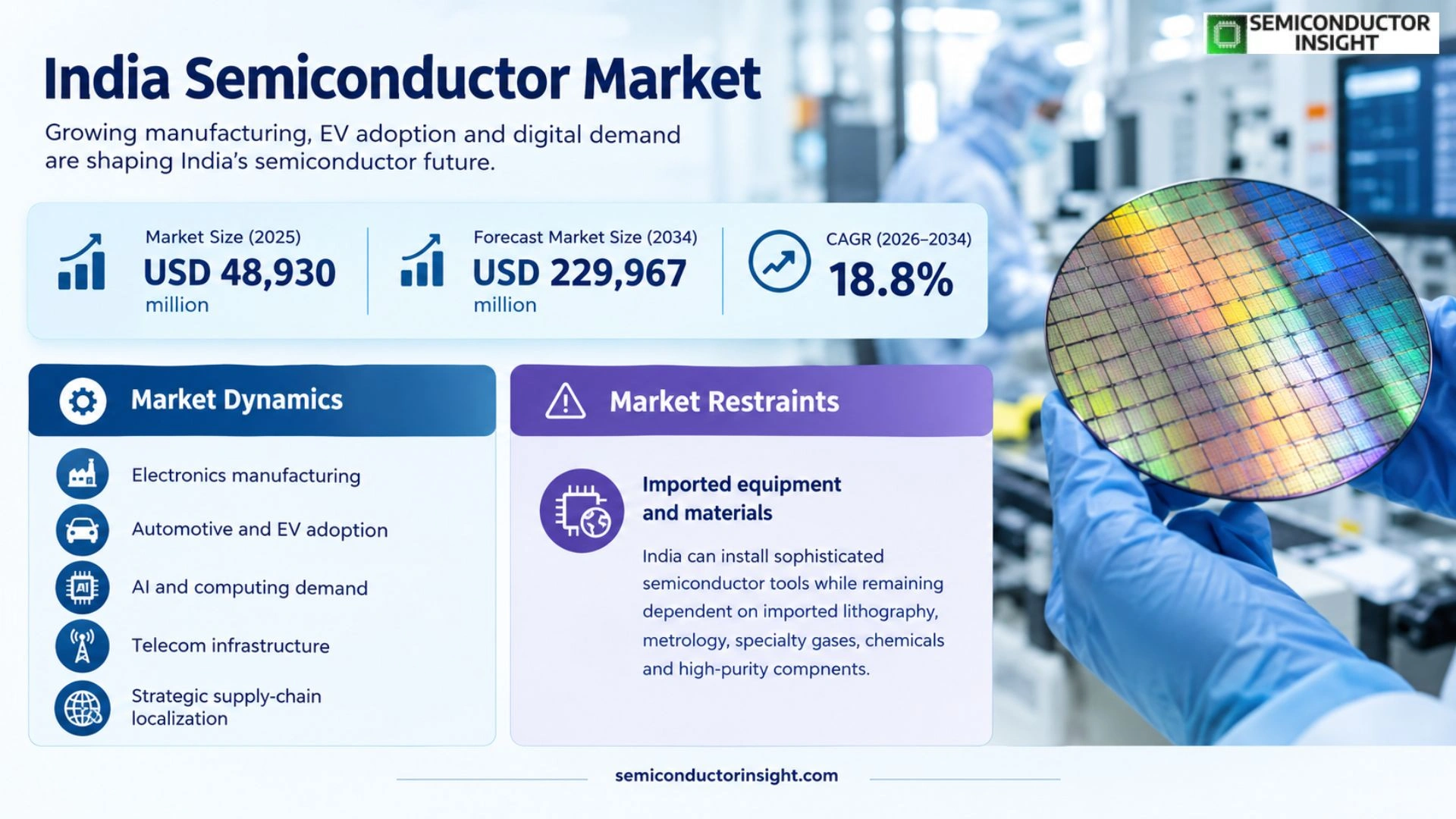
- USD 48,930 million in 2025 and 18.8% CAGR. India is moving from semiconductor consumption toward local fabrication, packaging, testing and design capacity.
- ICs remain the demand anchor. Computing, telecom, automotive, industrial and consumer electronics create the broadest component requirement, while process technology is central to domestic manufacturing capability.
- ₹1.6 lakh crore across 10 approved projects. The February 2026 project pipeline included 2 fabs and 8 packaging units, giving the ecosystem a broader industrial base.
- Gujarat is the leading production cluster. Dholera targets 50,000 wafer starts per month, while Micron and CG Semi add large-scale packaging and test in Sanand.
- Localization remains the main restraint. High-value equipment, specialty materials, gases and production know-how remain globally concentrated even as Indian capacity expands.
India Semiconductor Market Overview
India semiconductor market is USD 48,930 million in 2025 and USD 229,967 million by 2034, representing an 18.8% CAGR for 2026–2034. Asia Pacific is the largest regional context in the supplied scope, while India’s own ecosystem is being built around fabrication, assembly, test, packaging, design and downstream electronics manufacturing.
Base year: 2025 · Forecast period: 2026–2034 · Historical data: 2019–2024 · Values in USD million unless otherwise stated.
The market covers integrated circuits, optoelectronics, discrete semiconductors and sensors, with demand across consumer electronics, automotive, industrial, telecommunications, computing and healthcare. The commercial structure is changing because India is adding manufacturing capability to an ecosystem that already has substantial engineering and chip-design depth. This broadens the addressable value chain from imported component consumption into local packaging, assembly, testing, selected fabrication, materials support, equipment services and semiconductor-linked systems engineering.
The technology architecture is multi-layered. Semiconductor value is created through device design, wafer processing, fabrication, packaging, assembly, test, module integration and system qualification. India’s near-term economics are therefore not dependent on one cutting-edge process node. Mature-node, specialty, power, sensor and mixed-signal products can create commercial output while advanced front-end projects develop. Packaging and test can also monetize imported wafers while domestic fabrication capacity ramps, allowing the ecosystem to expand in stages rather than waiting for full vertical localization.
Government policy is now translating into physical infrastructure. The Semicon India Programme began with a ₹76,000 crore outlay, while the July 2026 Semicon 2.0 decision increased long-term support to ₹1,27,500 crore and explicitly widened the policy focus toward design, equipment, materials, Indian intellectual property and supply-chain resilience. For suppliers, that means each new semiconductor project creates adjacent opportunities in utilities, chemicals, gases, cleanroom services, metrology, packaging materials, maintenance, logistics and technical workforce development.
Segment Analysis: By Type
The supplied type segmentation contains four categories: integrated circuits, optoelectronics, discrete semiconductors and sensors. Integrated circuits provide the broadest demand base, while discrete devices and sensors provide important localization opportunities in power, automotive and industrial applications. The segment mix is therefore diversified by both device architecture and end use, which reduces the market’s dependence on a single semiconductor product family.
| Type | Function / Definition | Market position / demand characteristics |
|---|---|---|
| Integrated Circuits (ICs) | Integrated circuits combine processing, memory, control, power management or signal functions on semiconductor die and support the largest range of electronic applications. In India, demand spans computing, communications, automotive, industrial automation, consumer products and healthcare. Qualification depends on electrical performance, reliability, packaging, thermal characteristics and lifecycle support. The breadth of the category makes it the natural anchor for the market because one design or manufacturing capability can support several downstream industries across multiple 2025–2034 product cycles. | ICs provide the broadest commercial demand and remain the main device class around which local design, assembly and manufacturing capabilities can scale. India’s policy architecture also connects design-linked incentives with fabrication and packaging, making ICs central to both domestic supply and engineering exports. The competitive advantage increasingly rests on qualification, process stability, customer support and supply continuity rather than merely on unit cost, especially for automotive, telecom and industrial customers with long product lifetimes. |
| Optoelectronics | Optoelectronic devices convert, detect or modulate optical signals and serve communications, sensing, imaging and specialized industrial applications. The segment requires application-specific materials, packaging and test methods, so technical qualification can be more important than raw manufacturing volume. India’s opportunity is strongest where optical components can be integrated into modules, sensors or communications hardware and where local engineering can shorten development cycles. The commercial path includes both component manufacturing and specialized assembly rather than only high-volume wafer output. | Optoelectronics creates higher-value niches because customers often specify wavelength, efficiency, packaging and environmental performance rather than buying generic parts. This supports suppliers that can combine component knowledge with application engineering. India’s communications and sensing demand provides downstream opportunities, while global technology partnerships can supply upstream expertise. The market implication is that a focused optoelectronic capability can become commercially meaningful without requiring the same scale as a mainstream logic portfolio. |
| Discrete Semiconductors | Discrete semiconductors provide switching, rectification, amplification and power-conversion functions and are widely used in vehicles, chargers, industrial equipment, power supplies and appliances. Their economics are often tied to reliable electrical and thermal performance rather than transistor density. That makes mature processes, robust packaging and application-specific qualification commercially valuable. India’s expanding power-electronics and automotive ecosystems create a route for domestic suppliers to capture value in products that do not depend on the newest logic process generation. | Discrete devices are an important localization opportunity because they can support large installed bases of power electronics and industrial equipment without requiring the economics of the most advanced logic fabs. Suppliers can differentiate through voltage ratings, thermal performance, switching behavior, packaging and lifecycle support. The market implication is a broader domestic base that can serve automotive and industrial customers while reducing reliance on imported finished components in selected high-volume applications. |
| Sensors | Semiconductor sensors translate physical conditions such as pressure, temperature, motion, light or other variables into electrical signals. Indian demand is tied to automotive electronics, industrial automation, healthcare devices, connected systems and consumer products. Sensor commercialization depends on calibration, packaging, signal conditioning and environmental qualification, so the value proposition is often a combination of device and engineering support. As electronics become more instrumented, each additional sensing point increases component content and creates opportunities for localized specialty semiconductor production. | Sensors are a strategic growth niche because their demand follows the number of measured variables in vehicles, factories and connected products. Local suppliers can gain an advantage by providing calibration, module integration and application support alongside the sensor itself. That raises switching costs and can protect margins even when the underlying device technology is not cutting edge. The market implication is a pathway from semiconductor components into higher-value modules and system-level solutions. |
Technology differentiation
Process technology, packaging technology and fabrication technology interact throughout the Indian semiconductor value chain. A wafer process determines device structure and performance, packaging controls thermal and electrical behavior, and fabrication technology determines how the selected design is converted into repeatable production. The market opportunity therefore spans multiple technical layers. A supplier can create value by improving yield at a mature node, raising package reliability, localizing test services or supporting imported tools, even when the supplier is not building the most advanced transistor geometry.
India’s domestic capability is likely to remain mixed by application. Advanced computing and communications can require smaller geometries and sophisticated packaging, while automotive, power, sensing and industrial products can remain commercially attractive at mature or specialty processes with longer lifecycles. This diversity allows several investment models to coexist. The commercial question becomes whether a process can secure qualified customers, stable yields and reliable supply, not simply whether its nominal node number is smaller in 2025 or 2030.
Segment Analysis: By Application
Application demand spans consumer electronics, automotive, industrial, telecommunications, computing and healthcare. Consumer electronics supplies broad unit demand; automotive and industrial systems raise qualification and lifecycle requirements; telecommunications and computing increase demand for performance, memory, connectivity and power management. The purchasing mechanism therefore differs by application, with short-cycle consumer platforms contrasting with longer, qualification-heavy industrial and automotive programmes.
| Application | Demand characteristics |
|---|---|
| Consumer Electronics | Purchasing is driven by smartphones, appliances, televisions, wearables and personal electronics, where production volumes can change quickly with product cycles. Local manufacturing increases the number of nearby customers but does not automatically displace imported chips, so suppliers need to combine price, lead time, customization and reliable quality. Greenfield electronics factories are especially valuable because each new line introduces new component qualification events during 2025–2034. |
| Automotive | Automotive demand is driven by power management, sensing, control units, connectivity and electrification. Components face stricter temperature, reliability and traceability requirements than many consumer applications, creating longer qualification cycles. Indian suppliers that achieve automotive-grade quality can capture durable design wins because platforms can run for several model years. The commercial trigger is therefore a vehicle platform or subsystem award rather than a simple spot purchase, making early qualification strategically valuable. |
| Industrial | Industrial systems use semiconductors in drives, instrumentation, automation, power conversion and process control. Buyers emphasize stable supply, documentation and lifecycle support because equipment can remain installed for many years. Demand can be less volatile than consumer electronics but more specification-heavy. Local engineering and application support can therefore improve competitiveness, especially where customers want modified packages, customized devices or shorter service response rather than the absolute lowest unit price. |
| Telecommunications | Telecom equipment requires processors, RF devices, power management, optical components and control semiconductors. Network investment is cyclical, but the technical qualification barrier is high because failures affect large installed systems. Indian suppliers can participate through specialized ICs, power devices, sensors, packaging and module integration. Local supply becomes commercially attractive when it reduces lead time, improves resilience or supports equipment tailored to India’s operating conditions, power availability and deployment economics. |
| Computing | Computing demand includes processors, memory, connectivity, storage controllers, power-management devices and supporting components in PCs, servers and data centres. AI and accelerated computing increase semiconductor intensity at the system level. India’s most immediate opportunities include design, packaging, test, thermal and power support, and specialized devices around global compute platforms. The market implication is that local firms can capture value even before the country fabricates every advanced compute die domestically. |
| Healthcare | Medical electronics use sensors, controllers, power devices and communications components in imaging, monitoring and diagnostic systems. Purchasers value reliability, calibration, documentation and long availability, so qualified suppliers can maintain relationships across multiple equipment generations. Indian semiconductor and electronics companies can use local engineering support as a differentiator, especially where medical-device manufacturers need component changes or customized modules while maintaining controlled validation and long product lifecycles. |
Regional Analysis
The supplied scope lists North America, Europe, Asia Pacific, Middle East and Africa, and South Africa. For an India-specific market these are best interpreted as external ecosystem and customer contexts rather than Indian sub-national regions. The domestic manufacturing story itself is concentrated in Gujarat and Assam for large production projects, while design and engineering remain distributed across established technology centres. The regional picture therefore describes where India connects into the global semiconductor value chain.
How does India connect to the global semiconductor regional system?
India is building semiconductor capacity inside an already mature international network. North America supplies design, equipment, software and customer relationships; Europe contributes high-specification manufacturing technology; Asia Pacific provides the largest concentration of fabs, memory, packaging and electronics manufacturing; and Middle East and African markets provide downstream system demand. The commercial strategy is therefore integration: India gains value when domestic design and manufacturing can plug into established global standards while gradually localizing selected inputs and processes.
| Region | Position | Growth outlook | Demand profile | What decides supplier selection |
|---|---|---|---|---|
| Asia Pacific | Largest regional context | Highest strategic relevance | Fabs, packaging, electronics and supply chain | Process compatibility, cost, logistics, qualification and supply resilience matter because India must integrate into dense Asian networks. |
| North America | Major external ecosystem | Design and technology led | Compute, telecom, equipment and systems | IP discipline, quality, reliability, customer qualification and support determine access. |
| Europe | High-specification partner | Capability-transfer led | Equipment, industrial and precision applications | Traceability, process control, tool compatibility and long-term support are key. |
| Middle East & Africa | Emerging external market | Infrastructure and project led | Telecom, energy, industrial and digital systems | Distribution reach, application support and dependable delivery shape supplier selection. |
| South Africa | Focused reference market | Industrial-project linked | Mining, energy, telecom and industrial electronics | Robustness, lifecycle support and service availability matter more than pure volume. |
Competitive Landscape
Competition in India is an ecosystem contest involving semiconductor manufacturers, packaging and test companies, design houses, electronics manufacturers and global technology partners. Tata Electronics and Micron are building high-visibility manufacturing capacity, while CG Semi, CDIL, SPEL and other local participants contribute packaging or semiconductor manufacturing capability. HCL Technologies, Wipro, ASM Technologies and Saankhya Labs add engineering and design capacity. The most defensible positions will combine capital, technology partnerships, qualification capability and reliable production.
Tata Electronics has a strategically important position because its plans connect front-end fabrication with downstream semiconductor assembly and a broader electronics manufacturing base. Micron’s Sanand facility creates an export-oriented memory assembly and test anchor. CG Semi adds specialized OSAT capacity. These projects create not only production output but also an ecosystem of suppliers, technicians, maintenance companies and quality specialists, increasing the opportunity for second-tier domestic firms to capture value around the primary plants.
The competitive field also contains companies that do not own leading-edge fabrication but remain important to the semiconductor ecosystem. Design and engineering firms can monetize intellectual property and verification, while electronics manufacturers create downstream demand that improves the economics of domestic semiconductor content. This means market leadership cannot be judged by semiconductor wafer output alone. Qualification wins, engineering depth, customer relationships and access to large electronics programmes can become as strategically important as fab ownership.
Global suppliers remain essential partners because India’s domestic ecosystem does not yet replicate every equipment, materials and process technology layer. The commercial opportunity for local suppliers is therefore strongest where they can complement global technology: maintenance, utilities, cleanroom services, packaging materials, test, calibration, logistics and specialized engineering. Partnerships reduce the learning curve, but they also raise quality expectations because domestic facilities must operate to internationally familiar process and documentation standards.
Competitive differentiation should increasingly come from reliability and lifecycle support rather than price alone. Automotive and industrial customers require long availability and traceability, while consumer customers emphasize cost and refresh speed. Companies that can serve several application categories with stable manufacturing and local engineering can diversify their revenue base and reduce exposure to any one product cycle. The market implication is a multi-tier ecosystem where global anchors, domestic specialists and engineering firms play complementary roles.
| Tier | Companies / ecosystem role | Basis of competition |
|---|---|---|
| Manufacturing anchors | Tata Electronics; Micron Technology | Capital, fabrication or assembly capacity, global partnerships, customer qualification and ability to execute large projects. |
| Specialized semiconductor suppliers | Bharat Electronics; CDIL; SPEL Semiconductor | Device specialization, packaging/test capability, domestic customer access, lifecycle support and targeted manufacturing. |
| Engineering and design | HCL Technologies; Wipro; ASM Technologies; Saankhya Labs | Design, verification, embedded systems, semiconductor engineering and integration services rather than full wafer production. |
| Technology partners | Global equipment, materials and IP providers | Process technology, lithography, metrology, manufacturing know-how, equipment service and access to established global standards. |
The supplied company list includes HCL Technologies, Vedanta Ltd, Tata Electronics, Wipro, Micron Technology, Bharat Electronics Limited, ASM Technologies, Saankhya Labs, Continental Device India Pvt. Ltd., Dixon Technologies, ISMC Digital and SPEL Semiconductor, plus other key players. Because the list spans manufacturers, engineering firms and ecosystem participants, the competitive tiering above deliberately separates direct semiconductor suppliers from companies whose commercial role is design, electronics manufacturing or technology support. That distinction avoids treating every listed organization as an identical supplier category.
Companies covered in this report
| Company | Role Covered |
|---|---|
| HCL Technologies | Engineering and semiconductor-design services |
| Vedanta Ltd | Semiconductor ecosystem investment and materials/manufacturing ambitions |
| Tata Electronics | Semiconductor manufacturing and advanced packaging capacity |
| Wipro | Technology engineering and semiconductor-related services |
| Micron Technology | Memory assembly and test manufacturing in India |
| Bharat Electronics Limited (BEL) | Electronics and semiconductor-related manufacturing for strategic applications |
| ASM Technologies | Engineering, design and semiconductor services |
| Saankhya Labs | Semiconductor and communications-chip design |
| Continental Device India Pvt. Ltd. (CDIL) | Discrete semiconductor and device manufacturing |
| Dixon Technologies (India) Ltd. | Electronics manufacturing and downstream semiconductor demand |
| ISMC Digital | Semiconductor manufacturing project participant |
| SPEL Semiconductor | Semiconductor assembly and test services |
Production Capacity Analysis / Supply-Side Analysis
India’s supply-side expansion is now supported by project-level evidence rather than policy statements alone. Dholera provides the largest planned front-end capacity at 50,000 wafer starts per month, Micron’s Sanand facility adds large-scale DRAM and NAND assembly and test, Tata’s Assam unit is planned at 48 million units per day, and CG Semi’s Sanand unit is planned at 15 million units per day. These projects create demand for utilities, process chemicals, gases, maintenance, packaging materials, test equipment and skilled technicians.
The Dholera fab is associated with a ₹91,000 crore investment, 50,000 wafer starts per month, a 66.166-hectare SEZ footprint and an employment objective of 21,000 people. The project is therefore an industrial cluster, not merely a cleanroom. Supporting businesses will be needed for power quality, water treatment, chemicals, gases, waste management, tool maintenance, metrology and logistics. The commercial implication is that each unit of wafer capacity generates ancillary demand several steps upstream and downstream, creating a broad supplier opportunity.
Micron’s Sanand facility opened on 28 February 2026 and converts advanced DRAM and NAND wafers into finished memory and storage products. Micron describes more than 500,000 square feet of cleanroom space for the first phase and approximately USD2.75 billion of combined investment with government partners. Government information also cites ₹22,516 crore of approved investment and around 14 million units per week of production capacity. This gives India a significant export-oriented anchor for memory assembly, test, materials, logistics and technical services.
Tata Semiconductor Assembly and Test’s Assam project is designed around ₹27,000 crore of investment and 48 million units per day of planned capacity, with 15,000 direct and 11,000–13,000 indirect jobs cited in government approval information. CG Semi’s Sanand project adds ₹7,600 crore and 15 million units per day of planned capacity. The combination of Gujarat and Assam reduces geographic concentration and creates two major packaging clusters, which is commercially valuable for supply resilience and workforce development.
Upstream localization remains the main supply-side constraint. A fab can operate with imported lithography tools, specialty chemicals, gases, substrates and spare parts, but dependence on international inputs leaves production exposed to logistics disruption and supplier concentration. Domestic companies can capture value first in support categories where qualification requirements are achievable: utilities, maintenance, packaging materials, waste treatment, equipment service and local logistics. The market implication is that semiconductor supply-chain localization is broader than semiconductor fabrication itself.
Workforce capability is another capacity constraint. Semiconductor plants require technicians, process engineers, quality specialists, equipment engineers and managers who understand high-purity production, statistical process control and equipment uptime. Policy targets can finance training, but factory learning requires actual production experience across 2026–2034. The commercial opportunity is therefore growing for training companies, equipment service providers and technical contractors that can shorten the ramp from installed capacity to stable yield and customer-qualified output.
Market Dynamics
The market is pulled by electronics manufacturing, automotive and EV adoption, AI and computing demand, telecom infrastructure and strategic supply-chain localization. Policy support lowers investment barriers, while large fab and OSAT projects create new local production nodes. The main counterforces are capital intensity, imported materials and equipment, workforce scarcity and qualification timelines. The result is a high-growth ecosystem market in which execution quality and supply-chain depth determine how quickly announced capacity becomes commercially useful.
Market Drivers
| Factor | Relative impact | Geographic relevance | Impact timeline | Commercial interpretation |
|---|---|---|---|---|
| Government ecosystem support | High | India-wide | 2021–2034 | ₹76,000 crore initial programme and ₹1,27,500 crore Semicon 2.0 support reduce project risk and broaden the investment base. |
| Electronics manufacturing | High | National production clusters | 2025–2034 | More local electronics assembly raises semiconductor content and creates customer proximity for domestic suppliers. |
| Automotive and EV electronics | Medium-High | Automotive clusters | 2025–2034 | Sensors, power devices and controllers gain importance as vehicle electronics content rises. |
| AI, computing and telecom | High | National and export linked | 2026–2034 | AI and connected infrastructure raise demand for processors, memory, networking, power and supporting semiconductors. |
Government ecosystem support
India’s semiconductor policy has moved from a single incentive pool toward a broader ecosystem programme. The original ₹76,000 crore Semicon India structure targeted manufacturing, while the 15 July 2026 Semicon 2.0 decision announced a ₹1,27,500 crore outlay covering design, equipment, materials and Indian IP. This changes the supplier opportunity because support now extends into more stages of the value chain. The market effect is a larger and potentially longer investment pipeline spanning fabs, OSAT, materials and design through 2034.
Electronics manufacturing
Semiconductor demand follows electronics production because each system requires processing, memory, power, sensing and connectivity components. Greenfield electronics factories create new qualification events, while expanding installed production increases recurring replacement and support demand. The commercial response is localization around the final assembly base: domestic package and test operations can reduce logistics friction and enable customization even when wafers or some ICs remain imported. The market implication is that semiconductor consumption can rise alongside electronics output before complete vertical integration is achieved.
Automotive and EV electronics
Vehicle electrification increases semiconductor intensity through traction control, battery management, sensing, power conversion, connectivity and digital control. Automotive customers also create longer lifecycles because safety and reliability qualification are demanding. Suppliers therefore respond with robust packaging, traceability and application support. The market implication is a durable demand stream for discrete, sensor, analog and mixed-signal devices that can complement higher-volume consumer electronics demand and give domestic semiconductor suppliers additional design-win opportunities.
AI, computing and telecom
AI infrastructure increases semiconductor content across compute, memory, networking, power management and thermal management. India can participate in this expansion through design, packaging, testing and supporting components even when the most advanced accelerator dies remain externally sourced. The commercial response is to build capability around global platforms. The market implication is that local value capture can occur in multiple layers, increasing the addressable market for domestic suppliers and technical services as AI deployment scales.
Market Restraints
| Factor | Relative impact | Geographic relevance | Impact timeline | Evidence-based interpretation |
|---|---|---|---|---|
| Imported equipment and materials | High | National | 2025–2034 | Fabs and OSAT sites remain connected to internationally concentrated tools, gases, chemicals, wafers and specialty inputs. |
| Capital and execution risk | High | Fab and OSAT clusters | 2025–2034 | Large projects require long ramp periods, qualified customers, utilities and high utilization. |
| Workforce constraints | Medium-High | Major semiconductor clusters | 2025–2034 | Production requires specialized engineers, technicians, quality staff and equipment specialists. |
| Qualification timelines | Medium | Automotive, telecom, industrial | 2025–2034 | Domestic suppliers need reliability and lifecycle evidence before displacing established global components. |
Imported equipment and materials
India can install sophisticated semiconductor tools while remaining dependent on imported lithography, metrology, specialty gases, chemicals and high-purity components. The immediate commercial response is localization of support services, inventory and selected consumables while maintaining qualified international inputs. The restraint is therefore not an absence of manufacturing capability but exposure to upstream concentration. The market implication is that supply-chain resilience will improve incrementally and will require investment beyond the cleanroom itself.
Capital and execution risk
Semiconductor projects require large investments before reliable yield and customer qualification are established. A fab can be physically complete while utilization remains low if customer demand, process maturity or product qualification lags. Investors and suppliers therefore value anchor customers, credible technology partners and phased capacity ramps. The restraint matters because the 2025–2034 opportunity is large, but the commercial return depends on turning capital into qualified, high-utilization production rather than simply adding installed capacity.
Workforce constraints
Semiconductor production requires skills that are not interchangeable with general electronics assembly. Operators must understand high-purity environments, process windows, statistical control, equipment maintenance and defect reduction, while engineers need experience with specific tools and materials. The commercial response is joint training, international partnerships and supplier-service expansion. The market implication is that workforce capacity can limit throughput even when cleanroom space and equipment are already in place, particularly during simultaneous ramps across Gujarat and Assam.
Qualification timelines
Automotive, industrial and telecom customers often maintain long component-qualification cycles because a failure can cause downtime, recalls or system redesign. New Indian suppliers must therefore prove stable lots, reliability, traceability and lifecycle support before replacing established brands. The commercial implication is that early design wins have disproportionate strategic value because one qualified customer can become a reference that supports additional programs and helps stabilize utilization of new domestic semiconductor capacity.
Market Opportunities
Gujarat semiconductor cluster
Where: Dholera and Sanand. Who benefits: fabs, OSAT companies, equipment services, chemicals, utilities, packaging materials and logistics providers. What changes: 2026 project activity converts policy into clustered production demand. Commercial implication: suppliers can serve multiple semiconductor customers from one ecosystem, improving utilization of service teams and creating reference qualifications that can support expansion through 2028, 2030 and 2034.
Assam packaging cluster
Where: Morigaon, Assam. Who benefits: packaging, test, utilities, workforce and logistics suppliers. What changes: a planned 48 million-unit-per-day operation expands semiconductor production beyond western India. Commercial implication: domestic suppliers can build a second regional hub, reducing geographic concentration while creating an eastern demand center for materials, maintenance and downstream electronics support.
Design and Indian IP
Where: Bengaluru, Hyderabad, Noida and other engineering centers. Who benefits: chip-design firms, IP developers, verification providers and embedded-system companies. What changes: Semicon 2.0 expands policy focus on design and Indian IP. Commercial implication: companies can monetize engineering capability before owning large front-end capacity, building a bridge between software-led semiconductor value and physical manufacturing.
Power, sensing and specialty devices
Where: automotive, industrial and energy clusters nationwide. Who benefits: discrete, sensor, analog and mixed-signal manufacturers. What changes: electrification, automation and infrastructure increase device content. Commercial implication: mature and specialty processes can reach meaningful utilization without requiring the economics of the smallest logic nodes, provided suppliers secure long-cycle qualification and reliable customers.
Supply Chain Analysis
Upstream
Upstream supply remains internationally connected because wafers, lithography, metrology, specialty chemicals and gases are produced by concentrated supplier bases. Indian localization therefore starts with supporting infrastructure rather than complete substitution. Domestic companies can enter through utilities, maintenance, waste treatment, logistics and selected materials where qualification requirements are achievable. The commercial opportunity grows as semiconductor capacity expands from 2025 through 2034 because every production line increases recurring demand for qualified inputs and services.
Manufacturing
Manufacturing is developing through a combination of front-end fabrication and back-end assembly and test. Dholera contributes planned wafer capacity, while Sanand and Assam expand packaging. The layered structure creates a market for process services, test equipment, package materials and engineering. Commercial value is captured at several points, so domestic suppliers can participate without owning the full chain. The market implication is a gradual shift toward deeper local value capture rather than an immediate all-or-nothing localization model.
Channel
The channel layer connects semiconductor suppliers with electronics manufacturers and system integrators. Forecast visibility matters because customers plan component needs months or years ahead, while new design wins can take long qualification cycles. Indian suppliers therefore need inventory discipline, technical support and predictable lead times. Distributors become more valuable when products require application guidance. The commercial implication is that channel strength can determine how quickly a newly qualified domestic semiconductor product translates into recurring volume.
Downstream
Downstream demand is diversified across consumer, automotive, telecom, computing, industrial and healthcare markets. Each application adds different requirements for performance, reliability, cost and lifecycle. This diversity helps the semiconductor market because weakness in one segment can be offset by another, but it also forces suppliers to maintain multiple qualification paths. The commercial opportunity is strongest where a domestic semiconductor product can be reused across several applications, improving manufacturing utilization and reducing dependence on one customer programme.
Recent Developments
- 15 July 2026 Announced
Cabinet approves Semicon 2.0 with ₹1,27,500 crore outlay. The programme expands support into design, equipment, materials, Indian IP and supply-chain resilience; government information also cites 105 startups developing chips. The market significance is a broader long-duration policy platform for 2026–2034 semiconductor investment. Official Source: Press Information Bureau
- 4 July 2026 Completed
CG Semi begins commercial production at Sanand. The OSAT facility became the third major Indian semiconductor facility to begin commercial chip packaging, creating an operating production reference and strengthening supplier, workforce and customer-qualification demand around Gujarat. Official Source: Press Information Bureau
- 16 May 2026 Announced
Tata Electronics and ASML sign agreement supporting the Dholera fab. The relationship connects India’s planned front-end fab with ASML lithography technology. It matters because it ties domestic manufacturing investment to global equipment standards and creates demand for local engineering, utilities and process-support capabilities. Official Source: Press Information Bureau
- 28 February 2026 Completed
Micron opens India’s first semiconductor assembly and test facility. The Sanand facility converts DRAM and NAND wafers into finished memory and storage products and is planned to exceed 500,000 square feet of cleanroom space in its first phase. Micron describes approximately USD2.75 billion of combined investment with government partners. Official Source: Micron Technology
- 4 February 2026 Published
Government reports 10 approved semiconductor projects with about ₹1.6 lakh crore of envisaged investment. The project pipeline included 2 fabs and 8 packaging units. The combination is significant because it creates simultaneous demand for fabrication, packaging, equipment, materials, utilities and technical services rather than relying on one flagship facility. Official Source: Press Information Bureau
Report Scope & Segmentation
| Attribute | Scope definition |
|---|---|
| Study Period | 2019–2034, using the supplied historical scope and the target 2025–2034 overview window. |
| Base Year | 2025; USD48,930 million. |
| Estimated Year | 2025. |
| Forecast Period | 2026–2034. |
| Historical Period | 2019–2024. |
| Market Size | USD48,930 million in 2025 and USD229,967 million in 2034. |
| Growth Rate | 18.8% CAGR for 2026–2034. |
| Unit | USD million unless otherwise stated; capacity figures use their published units. |
| By Type | Integrated Circuits (ICs); Optoelectronics; Discrete Semiconductors; Sensors. |
| By Application | Consumer Electronics; Automotive; Industrial; Telecommunications; Computing; Healthcare. |
| By Technology | Process Technology; Packaging Technology; Fabrication Technology. |
| By End User | Automotive & Transportation; Telecommunications; Consumer Electronics; Industrial Automation & Manufacturing; Healthcare & Medical Devices. |
| By Region | North America; Europe; Asia Pacific; Middle East and Africa; South Africa, as listed in the supplied scope. |
| Key Companies Profiled | HCL Technologies; Vedanta Ltd; Tata Electronics; Wipro; Micron Technology; Bharat Electronics Limited (BEL); ASM Technologies; Saankhya Labs; Continental Device India Pvt. Ltd. (CDIL); Dixon Technologies (India) Ltd.; ISMC Digital; SPEL Semiconductor; Other Key Players. |
| Customization Scope | Analysis may be extended by state cluster, device category, technology, production capacity, end use, customer qualification and supply-chain stage. |
Frequently Asked Questions
What is the India semiconductor market size in 2025?
The India semiconductor market size is USD48,930 million in 2025. This is the starting point for the 2026–2034 overview and is paired with an 18.8% CAGR and a 2034 endpoint of USD229,967 million. The scope covers integrated circuits, optoelectronics, discrete semiconductors and sensors serving consumer electronics, automotive, industrial, telecom, computing and healthcare applications.
What is the India semiconductor market size in 2034?
The market is projected to reach USD229,967 million in 2034 during the 2026–2034 forecast period. The endpoint follows the same compound growth path used across the report, keeping the market-size figures consistent in the Key Statistics, Market Overview, Scope table and FAQ. The forecast reflects expanding domestic manufacturing, electronics demand, semiconductor content and ecosystem investment rather than a single product segment.
What is the CAGR of the India semiconductor market from 2026 to 2034?
The reported CAGR is 18.8% for 2026–2034. This compound rate summarizes the target market trajectory and should not be read as identical annual growth for every device or application. Growth is expected to be supported by semiconductor project approvals, electronics manufacturing, automotive and EV electronics, computing and telecommunications, while capital intensity and imported upstream inputs moderate the pace.
Which product type leads the India semiconductor market?
Integrated circuits are the broadest product category in the supplied scope because they support computing, communications, automotive, industrial, consumer and healthcare systems. Their strategic importance is reinforced by India’s strong design base and by the policy objective of linking design, packaging, testing and fabrication. IC demand is therefore a central mechanism through which new semiconductor capacity can connect to multiple downstream markets.
Why is process technology important in India?
Process technology determines how semiconductor structures are built on wafers and influences performance, power, density, reliability and yield. India’s market is not limited to one node because automotive, industrial, power and sensor applications can use mature or specialty processes while advanced computing requires more sophisticated technologies. The commercial opportunity therefore spans several process levels and depends on qualified customers, stable yield and lifecycle support.
What applications drive India semiconductor demand?
Consumer electronics supplies broad unit demand, while automotive, telecom, computing and industrial systems increasingly add semiconductor content per finished system. Automotive brings long qualification and reliability requirements, while computing and telecom raise the need for processors, memory, connectivity and power management. Healthcare adds a smaller but specification-heavy stream. This diversified application mix creates several routes for domestic semiconductor suppliers to build utilization and design wins.
Where is semiconductor manufacturing growing in India?
Gujarat is the most visible current manufacturing cluster, combining Tata Electronics’ planned Dholera fab with Micron and CG Semi activities in Sanand. Assam adds a large packaging project through Tata Semiconductor Assembly and Test, while Karnataka and other technology centres remain important for design and engineering. The domestic market is therefore developing as a network of specialized hubs rather than a single semiconductor city.
What is the planned capacity of the Dholera fab?
The Tata Electronics Dholera project is planned for 50,000 wafer starts per month and is associated with a ₹91,000 crore investment. Government documents also cite a 66.166-hectare SEZ footprint and an employment objective of 21,000 people. The project’s scale makes it a demand anchor for semiconductor tools, chemicals, gases, utilities, cleanroom services, maintenance, logistics and technical workforce development.
What capacity does Micron have in India?
Micron’s Sanand assembly and test facility converts DRAM and NAND wafers into finished memory and storage products. Its first phase is planned to exceed 500,000 square feet of cleanroom space, while government information cites about 14 million units per week of production capacity and ₹22,516 crore of approved investment. Micron describes approximately USD2.75 billion of combined investment with government partners, positioning Sanand as an export-oriented ecosystem anchor.
What are the biggest restraints on the India semiconductor market?
The biggest constraints are imported equipment and materials, high capital requirements, specialized workforce needs and lengthy customer-qualification cycles. A fab can operate while still relying on globally sourced lithography, metrology, gases and chemicals, so supply-chain autonomy develops gradually. Domestic suppliers also need reliability evidence before replacing incumbents. The commercial response is localization of support categories, dual sourcing, workforce development and early anchor-customer engagement.

Get Sample Report PDF for Exclusive Insights
Report Sample Includes
- Table of Contents
- List of Tables & Figures
- Charts, Research Methodology, and more...
 Download Sample Report PDF