Key Statistics
Key Takeaways
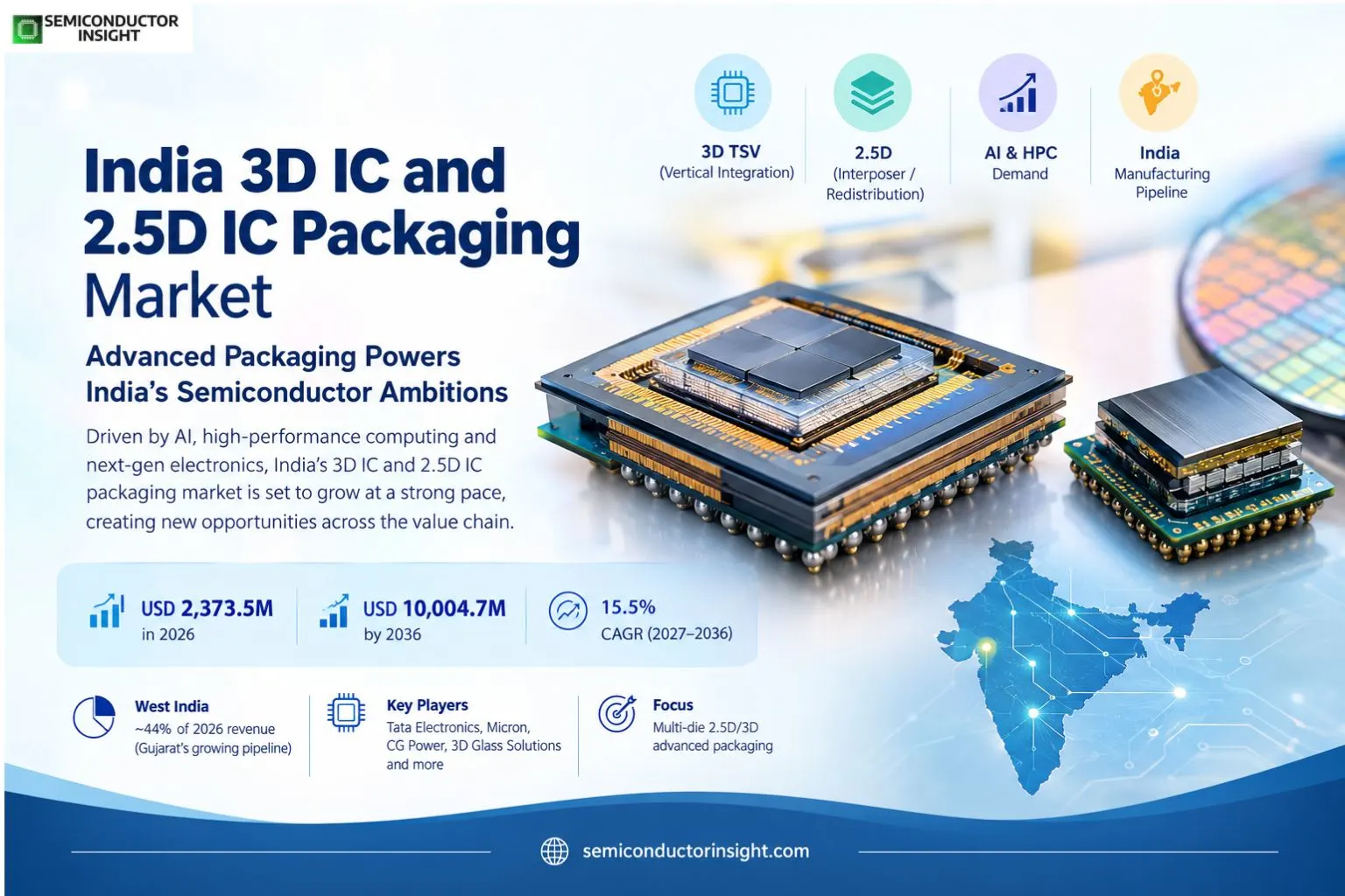
- Revenue outlook: India’s advanced 3D and 2.5D packaging market is valued at USD 2,373.5 million in 2026 and is projected at USD 10,004.7 million by 2036, implying 15.5% annualized growth. The boundary includes 3D TSV and 2.5D/3D wafer-level integration but excludes conventional single-die plastic packaging and separately purchased wafer fabrication equipment.
- Technology mix: 3D TSV architectures lead at an estimated ~58% of 2026 revenue and expand at ~16.2% CAGR, reflecting high-density memory and compute integration. Wafer-level and interposer-based 2.5D/3D packages represent ~42% and serve broader heterogeneous integration applications, with adoption shaped by thermal design and package substrate availability.
- Application concentration: Telecommunication and data-center-adjacent infrastructure account for an estimated ~27% of 2026 demand and grow at ~17.4% CAGR. Consumer electronics follow at ~24%, automotive at ~18%, and industrial smart technologies at ~13%. Each application has different qualification standards, package cost ceilings and production-volume requirements.
- India geography: West India leads with an estimated ~44% share, driven by Gujarat’s manufacturing investments, followed by South India at ~30% through semiconductor design and engineering. East India is a smaller but faster-developing manufacturing location, supported by Assam packaging and Odisha heterogeneous-integration projects.
- Technology constraints: Silicon interposers, through-silicon vias, redistribution layers, die stacking and hybrid bonding demand specialized process control. Official Indian projects range from memory assembly to glass-substrate integration, so announced package capacity must be interpreted by technology rather than treated as uniform 3D integration output.
India 3D IC and 2.5D IC Packaging Market Overview
India 3D IC and 2.5D IC packaging market was valued at USD 2,373.5 million in 2026 and is projected to reach USD 10,004.7 million by 2036, registering a CAGR of 15.5% during 2027–2036. West India holds an estimated ~44% of 2026 revenue, reflecting Gujarat’s expanding assembly, test and wafer-fabrication pipeline; however, the commercial scope is limited to advanced multi-die packaging rather than all domestic semiconductor output.
Advanced 2.5D packaging places multiple dies side by side on a silicon interposer, embedded bridge or redistribution structure; 3D integration stacks active dies vertically and can use through-silicon vias or hybrid bonding. These technologies connect logic, memory and specialized functions at shorter distances than conventional printed-circuit boards. The commercial boundary excludes ordinary leadframe packaging, wafer fabrication sold independently and capital equipment used to build packaging lines.
The distinction between 2.5D and 3D is more than geometry. A silicon interposer allows high-density lateral links between compute and high-bandwidth memory, while vertical stacking can reduce footprint and interconnect length at the cost of greater thermal concentration. Samsung’s I-Cube family illustrates interposer-based integration, its X-Cube addresses vertical stacking, and TSMC offers CoWoS, InFO and SoIC as differentiated package platforms.
India’s manufacturing pipeline now includes several complementary capabilities. Official project records list Tata Electronics in Gujarat and Assam, Micron in Sanand, CG Power with Renesas and Stars Microelectronics, and 3D Glass Solutions in Odisha. These investments vary by product: memory assembly, conventional OSAT, advanced flip-chip and heterogeneous integration have different process flows. Only the portions meeting multi-die 2.5D/3D definitions belong in this market.
Advanced package demand is driven by the rising bandwidth and power needs of AI processors, network equipment and sophisticated electronics. ASE’s FOCoS-Bridge with TSV, announced in May 2025, aims to shorten power delivery paths, while TSMC SoIC and Samsung X-Cube address dense vertical links. Design teams must jointly optimize thermal resistance, signal integrity, package warpage and known-good-die testing rather than selecting a substrate solely on unit price.
Domestic production opportunities are therefore staged. Near-term activity emphasizes engineering, testing, assembly and qualification; advanced glass and interposer projects could support more sophisticated packages over time. India’s Design Linked Incentive and ChipIN programs broaden access to EDA and prototyping, but commercial production still requires imported equipment, substrate supply, reliable bonding processes and customer-approved quality systems.
Segment Analysis: By Type
The two controlling technology families are 3D TSV and 2.5D/3D wafer-level chip-scale packaging. 3D TSV has an estimated ~58% of 2026 revenue and ~16.2% CAGR because high-density vertical integration supports memory and compute stacks. The wafer-level group contributes ~42%, encompassing redistribution and interposer methods for multiple dies that require a different balance of cost, heat and integration density.
| Technology | Integration approach | Market position |
|---|---|---|
| 3D TSV | 3D TSV uses vertical die stacking with through-silicon vias, microbumps or hybrid bonding. Its engineering value is higher interconnect density for memory and compute stacks, alongside thermal and yield challenges. It serves packages where conventional wire bonds or coarse-pitch substrates cannot meet the required interconnect density. For technology 3D TSV, commercialization depends on package yield, test coverage, interconnect integrity and thermal performance under the intended operating conditions. The economic outcome also reflects substrate availability, customer qualification time and whether production volumes justify dedicated assembly equipment. These considerations distinguish a validated advanced package from a laboratory demonstration or an announced investment. | An estimated ~58% of 2026 market revenue belongs to 3D TSV, growing at ~16.2% CAGR. The selection of this technology depends on die dimensions, yield, power delivery, manufacturing readiness and the customer’s package reliability specification. For market position 3D TSV, commercialization depends on package yield, test coverage, interconnect integrity and thermal performance under the intended operating conditions. Within the type profile for 3D TSV, the economic outcome also reflects substrate availability, customer qualification time and whether production volumes justify dedicated assembly equipment. Within the type profile for 3D TSV, these considerations distinguish a validated advanced package from a laboratory demonstration or an announced investment. |
| 2.5D and 3D Wafer-Level Chip-Scale Packaging (WLCSP) | 2.5D and 3D Wafer-Level Chip-Scale Packaging (WLCSP) uses wafer-level redistribution, interposers, bridges and fan-out integration. Its engineering value is heterogeneous logic-memory assemblies that trade footprint, bandwidth and manufacturing complexity. Within the type profile for 2.5D and 3D Wafer-Level Chip-Scale Packaging (WLCSP), it serves packages where conventional wire bonds or coarse-pitch substrates cannot meet the required interconnect density. For technology 2.5D and 3D Wafer-Level Chip-Scale Packaging (WLCSP), commercialization depends on package yield, test coverage, interconnect integrity and thermal performance under the intended operating conditions. Within the type profile for 2.5D and 3D Wafer-Level Chip-Scale Packaging (WLCSP), the economic outcome also reflects substrate availability, customer qualification time and whether production volumes justify dedicated assembly equipment. Within the type profile for 2.5D and 3D Wafer-Level Chip-Scale Packaging (WLCSP), these considerations distinguish a validated advanced package from a laboratory demonstration or an announced investment. | An estimated ~42% of 2026 market revenue belongs to 2.5D and 3D Wafer-Level Chip-Scale Packaging (WLCSP), growing at ~14.4% CAGR. Within the type profile for 2.5D and 3D Wafer-Level Chip-Scale Packaging (WLCSP), the selection of this technology depends on die dimensions, yield, power delivery, manufacturing readiness and the customer’s package reliability specification. For market position 2.5D and 3D Wafer-Level Chip-Scale Packaging (WLCSP), commercialization depends on package yield, test coverage, interconnect integrity and thermal performance under the intended operating conditions. Within the type profile for 2.5D and 3D Wafer-Level Chip-Scale Packaging (WLCSP), within the type profile for 2.5D and 3D Wafer-Level Chip-Scale Packaging (WLCSP), the economic outcome also reflects substrate availability, customer qualification time and whether production volumes justify dedicated assembly equipment. Within the type profile for 2.5D and 3D Wafer-Level Chip-Scale Packaging (WLCSP), within the type profile for 2.5D and 3D Wafer-Level Chip-Scale Packaging (WLCSP), these considerations distinguish a validated advanced package from a laboratory demonstration or an announced investment. |
3D TSV
3D TSV combines vertical die stacking with through-silicon vias, microbumps or hybrid bonding. The most demanding deployments involve higher interconnect density for memory and compute stacks, alongside thermal and yield challenges. Engineers must coordinate substrate routing, microbump placement, thermal interfaces and final test across multiple dies, making package co-design a commercial differentiator for advanced electronics suppliers.
The estimated 2026 revenue share of 3D TSV is ~58%, with modeled growth of ~16.2% per year. Global foundry and OSAT platforms provide much of the established process know-how; Indian firms are expanding the supporting design, reliability and assembly ecosystem. Manufacturing announcements should be interpreted through the specific processes each facility can qualify.
Estimated annual 2.5D/3D packaging revenue by segment (USD million)
The estimates below show distinct views of the same India market and should not be added across regional, technology, application or package-function groupings. Each series is an indicative revenue allocation rather than a company shipment ledger. Growth profiles reflect technology adoption, local qualification and application maturity, while the market total follows the published monetary anchors.
| Segment | 2026 | 2027 | 2028 | 2029 | 2030 | 2031 | 2032 | 2033 | 2034 | 2035 | 2036 |
|---|---|---|---|---|---|---|---|---|---|---|---|
| Indian region | |||||||||||
| West India | 1,044.3 | 1,216.7 | 1,417.4 | 1,651.3 | 1,923.7 | 2,241.2 | 2,610.9 | 3,041.7 | 3,543.6 | 4,128.3 | 4,809.5 |
| South India | 712.0 | 816.7 | 936.8 | 1,074.5 | 1,232.4 | 1,413.6 | 1,621.4 | 1,859.7 | 2,133.1 | 2,446.7 | 2,806.4 |
| North India | 284.8 | 325.5 | 372.1 | 425.3 | 486.1 | 555.7 | 635.1 | 725.9 | 829.7 | 948.4 | 1,084.0 |
| East India | 237.3 | 276.0 | 321.0 | 373.4 | 434.2 | 505.0 | 587.3 | 683.0 | 794.4 | 923.9 | 1,074.5 |
| Central India | 94.9 | 103.8 | 113.4 | 124.0 | 135.5 | 148.1 | 161.9 | 176.9 | 193.4 | 211.4 | 231.0 |
| Integration type | |||||||||||
| 3D TSV | 1,376.6 | 1,599.6 | 1,858.8 | 2,159.9 | 2,509.8 | 2,916.4 | 3,388.9 | 3,937.9 | 4,575.8 | 5,317.1 | 6,178.4 |
| 2.5D and 3D Wafer-Level Chip-Scale Packaging (WLCSP) | 996.9 | 1,140.4 | 1,304.6 | 1,492.5 | 1,707.4 | 1,953.3 | 2,234.6 | 2,556.4 | 2,924.5 | 3,345.6 | 3,827.4 |
| Application | |||||||||||
| Telecommunication | 640.8 | 752.4 | 883.3 | 1,036.9 | 1,217.4 | 1,429.2 | 1,677.9 | 1,969.8 | 2,312.6 | 2,715.0 | 3,187.4 |
| Consumer electronics | 569.6 | 653.9 | 750.7 | 861.8 | 989.4 | 1,135.8 | 1,303.9 | 1,496.9 | 1,718.4 | 1,972.8 | 2,264.7 |
| Automotive | 427.2 | 487.9 | 557.2 | 636.3 | 726.7 | 829.8 | 947.7 | 1,082.2 | 1,235.9 | 1,411.4 | 1,611.8 |
| Industrial sector and smart technologies | 308.6 | 353.9 | 405.9 | 465.6 | 534.1 | 612.6 | 702.6 | 805.9 | 924.4 | 1,060.2 | 1,216.1 |
| Military & aerospace | 237.3 | 273.0 | 313.9 | 361.0 | 415.1 | 477.4 | 549.0 | 631.4 | 726.1 | 835.0 | 960.2 |
| Medical devices | 189.9 | 218.2 | 250.7 | 288.0 | 330.9 | 380.3 | 436.9 | 502.0 | 576.8 | 662.8 | 761.5 |
| Package function | |||||||||||
| Silicon interposer and bridge | 878.2 | 1,014.3 | 1,171.5 | 1,353.1 | 1,562.9 | 1,805.1 | 2,084.9 | 2,408.0 | 2,781.3 | 3,212.4 | 3,710.3 |
| TSV die stacks | 712.0 | 822.4 | 949.9 | 1,097.1 | 1,267.2 | 1,463.6 | 1,690.5 | 1,952.5 | 2,255.1 | 2,604.6 | 3,008.4 |
| Fan-out redistribution integration | 545.9 | 630.5 | 728.3 | 841.1 | 971.5 | 1,122.1 | 1,296.0 | 1,496.9 | 1,728.9 | 1,996.9 | 2,306.4 |
| Other multi-die packages | 237.3 | 274.1 | 316.6 | 365.7 | 422.4 | 487.9 | 563.5 | 650.8 | 751.7 | 868.2 | 1,002.8 |
2.5D and 3D Wafer-Level Chip-Scale Packaging (WLCSP)
2.5D and 3D Wafer-Level Chip-Scale Packaging (WLCSP) combines wafer-level redistribution, interposers, bridges and fan-out integration. The most demanding deployments involve heterogeneous logic-memory assemblies that trade footprint, bandwidth and manufacturing complexity. Within the technology discussion of 2.5D and 3D Wafer-Level Chip-Scale Packaging (WLCSP), engineers must coordinate substrate routing, microbump placement, thermal interfaces and final test across multiple dies, making package co-design a commercial differentiator for advanced electronics suppliers.
The estimated 2026 revenue share of 2.5D and 3D Wafer-Level Chip-Scale Packaging (WLCSP) is ~42%, with modeled growth of ~14.4% per year. Within the technology discussion of 2.5D and 3D Wafer-Level Chip-Scale Packaging (WLCSP), global foundry and OSAT platforms provide much of the established process know-how; Indian firms are expanding the supporting design, reliability and assembly ecosystem. Within the technology discussion of 2.5D and 3D Wafer-Level Chip-Scale Packaging (WLCSP), manufacturing announcements should be interpreted through the specific processes each facility can qualify.
Segment Analysis: By Application
Application demand spans telecommunication, consumer electronics, automotive, industrial smart technologies, military and aerospace, and medical devices. Telecom-linked infrastructure is the largest group at an estimated ~27% of 2026 revenue, while consumer electronics contribute ~24% and automotive ~18%. Differences in reliability, thermal budget and product lifetime make package technology selection application-specific rather than uniform across the electronics sector.
| Application | Demand characteristics |
|---|---|
| Telecommunication | Telecommunication represents an estimated ~27% of 2026 advanced packaging demand, expanding at ~17.4% CAGR. Key product settings include network processors, AI data-center interconnect and infrastructure silicon, with purchase decisions shaped by high-bandwidth memory attachment and dense package routing. Customers assess the full device and package qualification, not just the advertised die stacking technique. |
| Consumer electronics | Consumer electronics represents an estimated ~24% of 2026 advanced packaging demand, expanding at ~14.8% CAGR. Key product settings include premium mobile, PC and wearable system packages, with purchase decisions shaped by miniaturization and reliable wafer-level processing. Within the application profile for Consumer electronics, customers assess the full device and package qualification, not just the advertised die stacking technique. |
| Automotive | Automotive represents an estimated ~18% of 2026 advanced packaging demand, expanding at ~14.2% CAGR. Key product settings include advanced driver-assistance and connected-vehicle electronics, with purchase decisions shaped by long life, thermal cycling and functional safety. Within the application profile for Automotive, customers assess the full device and package qualification, not just the advertised die stacking technique. For end market Automotive, commercialization depends on package yield, test coverage, interconnect integrity and thermal performance under the intended operating conditions. Within the application profile for Automotive, the economic outcome also reflects substrate availability, customer qualification time and whether production volumes justify dedicated assembly equipment. Within the application profile for Automotive, these considerations distinguish a validated advanced package from a laboratory demonstration or an announced investment. |
| Industrial sector and smart technologies | Industrial sector and smart technologies represents an estimated ~13% of 2026 advanced packaging demand, expanding at ~14.7% CAGR. Key product settings include industrial machine vision, automation and edge computing, with purchase decisions shaped by robust assembly and predictable component sourcing. Within the application profile for Industrial sector and smart technologies, customers assess the full device and package qualification, not just the advertised die stacking technique. |
| Military & aerospace | Military & aerospace represents an estimated ~10% of 2026 advanced packaging demand, expanding at ~15.0% CAGR. Key product settings include rugged signal processing and defense electronics, with purchase decisions shaped by traceability, screening and long product support. Within the application profile for Military & aerospace, customers assess the full device and package qualification, not just the advertised die stacking technique. |
| Medical devices | Medical devices represents an estimated ~8% of 2026 advanced packaging demand, expanding at ~14.9% CAGR. Key product settings include imaging systems, portable diagnostics and implantable electronics, with purchase decisions shaped by package integrity and regulated validation. Within the application profile for Medical devices, customers assess the full device and package qualification, not just the advertised die stacking technique. |
AI and high-performance networking intensify demand for high-density package links between logic and memory. Interposers and TSV stacks reduce physical separation but introduce power-delivery, warpage and heat-removal constraints. ASE, TSMC and Samsung offer differentiated platforms, and Indian system integrators must select a proven solution with suitable software and thermal support rather than treating all 2.5D packages as interchangeable.
Automotive, medical and aerospace applications require longer qualification than consumer products. Temperature cycling, mechanical stress, traceability and failure analysis may dominate procurement decisions even where advanced packages offer size or bandwidth advantages. Domestic testing capability can create commercial value before India establishes the entire high-density integration chain, provided suppliers document repeatable yields and reliability.
Regional Analysis
West India leads the domestic advanced packaging market with an estimated ~44% of 2026 revenue, followed by South India at ~30%. North India accounts for ~12%, East India ~10% and Central India ~4%. This distribution reflects the location of relevant manufacturing projects, package engineering and customer demand; the share estimates do not imply that all semiconductor packaging in a state uses 2.5D or 3D integration.
How do Indian regional clusters differ in advanced packaging readiness?
Gujarat’s semiconductor investment pipeline makes West India the largest packaging activity center, while Bengaluru and Hyderabad concentrate much of the design and verification work. The northeast and Odisha are attracting new projects, including one with explicit heterogeneous integration. Capacity announcements should be evaluated by process and qualification status because a conventional OSAT plant and a TSV stacking line serve different markets.
The geographic opportunity depends on access to package substrates, specialized equipment, skilled technicians and customer qualification programs. Advanced integration often requires overseas foundry or OSAT services even when the chip is designed in India. A five-region model therefore describes Indian commercial demand and capability rather than the location of every die in a finished 2.5D or 3D product.
| Region | Position | Growth outlook | Demand profile | What decides supplier selection |
|---|---|---|---|---|
| West India | Largest (~44%) | ~16.5% CAGR | Gujarat advanced assembly investments and the Dholera fab pipeline. The project’s relevance to advanced packaging depends on whether actual 2.5D interposers, redistribution structures or 3D TSV stacks are qualified, not merely on the presence of a semiconductor cleanroom. Procurement also weighs substrate traceability, defect screening and the ability to deliver consistent process yield. | process capability, substrate sourcing and OSAT customer qualification. Within the regional comparison for West India, the project’s relevance to advanced packaging depends on whether actual 2.5D interposers, redistribution structures or 3D TSV stacks are qualified, not merely on the presence of a semiconductor cleanroom. Within the regional comparison for West India, procurement also weighs substrate traceability, defect screening and the ability to deliver consistent process yield. |
| South India | Second largest (~30%) | ~14.7% CAGR | Bengaluru, Hyderabad and Chennai package-design and system-engineering teams. Within the regional comparison for South India, the project’s relevance to advanced packaging depends on whether actual 2.5D interposers, redistribution structures or 3D TSV stacks are qualified, not merely on the presence of a semiconductor cleanroom. Within the regional comparison for South India, procurement also weighs substrate traceability, defect screening and the ability to deliver consistent process yield. | design-for-assembly, interconnect simulation and reliability test. Within the regional comparison for South India, within the regional comparison for South India, the project’s relevance to advanced packaging depends on whether actual 2.5D interposers, redistribution structures or 3D TSV stacks are qualified, not merely on the presence of a semiconductor cleanroom. Within the regional comparison for South India, within the regional comparison for South India, procurement also weighs substrate traceability, defect screening and the ability to deliver consistent process yield. |
| North India | Third largest (~12%) | ~14.3% CAGR | Noida electronics services and an approved Uttar Pradesh manufacturing investment. Within the regional comparison for North India, the project’s relevance to advanced packaging depends on whether actual 2.5D interposers, redistribution structures or 3D TSV stacks are qualified, not merely on the presence of a semiconductor cleanroom. Within the regional comparison for North India, procurement also weighs substrate traceability, defect screening and the ability to deliver consistent process yield. | engineering validation and package test infrastructure. Within the regional comparison for North India, within the regional comparison for North India, the project’s relevance to advanced packaging depends on whether actual 2.5D interposers, redistribution structures or 3D TSV stacks are qualified, not merely on the presence of a semiconductor cleanroom. Within the regional comparison for North India, within the regional comparison for North India, procurement also weighs substrate traceability, defect screening and the ability to deliver consistent process yield. |
| East India | Fourth largest (~10%) | ~16.3% CAGR | Assam assembly investment and Odisha glass-substrate heterogeneous integration. Within the regional comparison for East India, the project’s relevance to advanced packaging depends on whether actual 2.5D interposers, redistribution structures or 3D TSV stacks are qualified, not merely on the presence of a semiconductor cleanroom. Within the regional comparison for East India, procurement also weighs substrate traceability, defect screening and the ability to deliver consistent process yield. | manufacturing ramp and process-transfer validation. Within the regional comparison for East India, within the regional comparison for East India, the project’s relevance to advanced packaging depends on whether actual 2.5D interposers, redistribution structures or 3D TSV stacks are qualified, not merely on the presence of a semiconductor cleanroom. Within the regional comparison for East India, within the regional comparison for East India, procurement also weighs substrate traceability, defect screening and the ability to deliver consistent process yield. For region East India qualification, commercialization depends on package yield, test coverage, interconnect integrity and thermal performance under the intended operating conditions. Within the regional comparison for East India, the economic outcome also reflects substrate availability, customer qualification time and whether production volumes justify dedicated assembly equipment. Within the regional comparison for East India, these considerations distinguish a validated advanced package from a laboratory demonstration or an announced investment. |
| Central India | Fifth largest (~4%) | ~9.3% CAGR | smaller industrial electronics and component procurement clusters. Within the regional comparison for Central India, the project’s relevance to advanced packaging depends on whether actual 2.5D interposers, redistribution structures or 3D TSV stacks are qualified, not merely on the presence of a semiconductor cleanroom. Within the regional comparison for Central India, procurement also weighs substrate traceability, defect screening and the ability to deliver consistent process yield. | access to qualified packages from external vendors. Within the regional comparison for Central India, within the regional comparison for Central India, the project’s relevance to advanced packaging depends on whether actual 2.5D interposers, redistribution structures or 3D TSV stacks are qualified, not merely on the presence of a semiconductor cleanroom. Within the regional comparison for Central India, within the regional comparison for Central India, procurement also weighs substrate traceability, defect screening and the ability to deliver consistent process yield. |
India Advanced Packaging Suppliers and Competitive Landscape
The advanced packaging value chain is divided among foundries, OSAT providers, process-equipment suppliers, package designers and end-user chip companies. TSMC, Samsung, ASE and Intel have established 2.5D and 3D integration platforms, while Indian investments by Tata Electronics, CG Power and Micron build complementary local capabilities. Competitive positioning should be assessed by qualified process technology rather than total company revenue or generic semiconductor output.
TSMC 3DFabric combines CoWoS, InFO and SoIC, addressing different combinations of interposer integration, fan-out and vertical stacking. Samsung offers I-Cube and X-Cube platforms, with distinct lateral and vertical architectures. Customers compare wiring density, thermal resistance, known-good-die yield and production availability, so platform choice often becomes a long-term supply-chain decision rather than a simple assembly price comparison.
ASE VIPack integrates fan-out, embedded bridges and TSV-based 2.5D and 3D technologies. Its FOCoS-Bridge with TSV was announced in May 2025 to improve power delivery and dense interconnect performance for AI packages. Intel Foundry also develops Foveros and EMIB technologies, demonstrating alternative integration routes. Indian package designers must coordinate design rules and verification with the chosen supplier early in development.
India’s CG Power–Renesas–Stars venture plans a mix of QFN, QFP, FC-BGA and FC-CSP packages, while Micron’s Sanand site handles DRAM and NAND assembly and test. These investments contribute to workforce and process capability but should not all be booked as advanced multi-die revenue. The emerging supplier landscape includes specialized glass-substrate and heterogeneous integration projects whose production readiness must be demonstrated separately.
Tier structure
| Tier | Companies | Basis of competition |
|---|---|---|
| Global integration platforms | TSMC, Samsung Electronics, Intel Foundry, ASE Technology | Foundries and OSAT firms with established interposer, bridge, fan-out and vertical stacking processes compete on package density, yield, thermal performance and delivery scale. Their qualification rules and process design kits determine the practical availability of advanced packages to Indian customers. For tier global, commercialization depends on package yield, test coverage, interconnect integrity and thermal performance under the intended operating conditions. Within the supplier tier Global integration platforms, the economic outcome also reflects substrate availability, customer qualification time and whether production volumes justify dedicated assembly equipment. Within the supplier tier Global integration platforms, these considerations distinguish a validated advanced package from a laboratory demonstration or an announced investment. |
| Indian manufacturing pipeline | Tata Electronics, CG Power, Renesas, Micron, 3D Glass Solutions | Domestic investments expand fabrication, conventional assembly, test and selected heterogeneous integration capabilities. They differ materially in process scope, and approved investment figures should not be converted into chiplet package revenue without evidence of actual qualified products. For tier India, commercialization depends on package yield, test coverage, interconnect integrity and thermal performance under the intended operating conditions. Within the supplier tier Indian manufacturing pipeline, the economic outcome also reflects substrate availability, customer qualification time and whether production volumes justify dedicated assembly equipment. Within the supplier tier Indian manufacturing pipeline, these considerations distinguish a validated advanced package from a laboratory demonstration or an announced investment. |
| Design and materials ecosystem | Arm, Cadence, Synopsys, UCIe members, substrate suppliers | Design IP, interconnect standards, EDA tools and package substrates support multi-die co-design. This ecosystem enables package validation and supplier interoperability, but participants do not all sell finished advanced packages; customer contracts and tested manufacturing capabilities determine their commercial roles. For tier ecosystem, commercialization depends on package yield, test coverage, interconnect integrity and thermal performance under the intended operating conditions. Within the supplier tier Design and materials ecosystem, the economic outcome also reflects substrate availability, customer qualification time and whether production volumes justify dedicated assembly equipment. Within the supplier tier Design and materials ecosystem, these considerations distinguish a validated advanced package from a laboratory demonstration or an announced investment. |
Key companies profiled
- TSMC
- Samsung Electronics
- ASE Technology
- Intel Foundry
- Tata Electronics
- CG Power
- Renesas Electronics
- Micron Technology
- 3D Glass Solutions
- Arm
- Cadence Design Systems
- Synopsys
- Applied Materials
- Lam Research
India 3D IC and 2.5D IC Packaging Capacity and Technology Readiness
India is building wafer fabrication and outsourced assembly and test capacity, but the technologies approved under national programs range from conventional packages to specialized heterogeneous integration. The Gujarat and Assam projects provide scale, while Odisha’s glass substrate investment points toward advanced integration. Commercial 2.5D and 3D capacity depends on verified interposer routing, TSV or hybrid bonding, thermal qualification and known-good-die test.
The Government of India lists a Tata Electronics Gujarat fab investment of INR 91,526 crore with a target of 50,000 wafer starts per month, and an Assam packaging project of INR 27,120 crore with stated capacity of 48 million units per day. These figures describe approved projects with different technologies; neither number alone indicates how many 3D TSV packages will be delivered.
Micron opened its Sanand assembly and test site in February 2026, with more than 500,000 square feet of cleanroom space planned for the first phase after ramp-up. CG Power, Renesas and Stars Microelectronics plan a Gujarat OSAT facility with FC-BGA and FC-CSP capability. Such investments improve process control and test capacity, but qualification of advanced interposer or stacked-die products remains product-specific.
Odisha’s approved 3D Glass Solutions project explicitly includes glass panel substrate production and heterogeneous integration, a distinct technical opportunity within advanced packaging. Commercial success depends on substrate flatness, coefficient-of-thermal-expansion control, fine-pitch routing, bonding yield and customer validation. The ability to manufacture glass panels does not by itself establish high-volume 2.5D or 3D packaged IC output.
India 3D and 2.5D Packaging Market Dynamics
The main drivers are AI and high-performance computing, demand for smaller electronic systems, government-supported semiconductor investment and growing availability of design tools. Restraints include expensive process equipment, high-density substrate supply, die stacking yield and thermal stress. Opportunities center on interposer services, glass substrates, advanced test and co-design partnerships that can move India from conventional assembly toward qualified heterogeneous integration.
MARKET DRIVERS
Drivers Impact Analysis*
| Driver | (~) % impact on CAGR forecast | Geographic relevance | Impact timeline |
|---|---|---|---|
| AI and high-bandwidth integration | +2.6% | National telecom and compute buyers | Medium term (2027–2032) |
| Semiconductor manufacturing investments | +1.8% | West and East India | Long term (2027–2036) |
| Design and prototyping support | +1.1% | South and North India | Medium term (2027–2033) |
High-bandwidth logic and memory integration
AI processors and networking devices require denser links between compute dies and memory stacks than conventional board-level connections can provide. TSMC CoWoS and Samsung I-Cube illustrate lateral integration, while 3D stacking can shorten paths further. Indian systems companies benefit through access to qualified imported packages and future domestic engineering opportunities, but thermal and power-delivery constraints must be addressed early.
Public investment expands assembly capability
Approved projects in Gujarat, Assam and Odisha are adding or planning semiconductor facilities with different manufacturing scopes. The new infrastructure can attract materials, test, reliability and design-service providers, creating an ecosystem in which advanced packages become more feasible. Only verified multi-die process capability should be included in the advanced packaging revenue boundary, because conventional assembly remains a separate market.
Package co-design reduces integration risk
EDA access and design-for-test tools help teams coordinate silicon, substrate and thermal requirements before a product reaches assembly. ASE’s integrated design ecosystem and UCIe’s packaging-related specification work show how interface planning can shorten development cycles. Indian firms can specialize in package verification and qualification services while partnering with established global manufacturers for complex bonding operations.
MARKET RESTRAINTS
Restraints Impact Analysis*
| Restraint | (~) % impact on CAGR forecast | Geographic relevance | Impact timeline |
|---|---|---|---|
| Expensive interposers and bonding tools | −1.9% | All regions; highest in AI systems | Medium term (2027–2033) |
| Substrate and materials supply risk | −1.3% | West, South and East India | Long term (2027–2036) |
| Reliability and thermal constraints | −1.0% | Automotive, medical and defense | Medium term (2028–2034) |
Advanced integration carries a steep cost curve
Silicon interposers, TSV etching, fine-pitch redistribution and hybrid bonding require specialized equipment and strict process control. These steps can raise package cost and reduce yield when die quality or substrate flatness is inconsistent. Indian manufacturers must establish repeatable inspection and failure analysis before customers accept volume commitments, especially for complex multi-die AI packages.
Materials and equipment remain globally concentrated
High-density package substrates, bonding equipment and specialized test tools are sourced from a relatively small global supplier base. Even with domestic assembly investment, delays in imported components can extend qualification and ramp schedules. The commercial risk is greatest when a customer has designed around one proprietary interposer platform and cannot transfer the package to an alternate OSAT quickly.
Thermal density complicates stacked-die products
3D packages shorten signal paths but concentrate heat within stacked silicon layers, while large 2.5D interposers can create warpage and mechanical stress. Automotive and medical buyers demand documented reliability across temperature and operating conditions. A successful package therefore requires integrated thermal, mechanical and electrical simulation rather than treating a higher interconnect count as sufficient evidence of suitability.
MARKET OPPORTUNITIES
Glass substrates and alternative interposers
Odisha’s heterogeneous integration and glass-panel substrate project points to opportunities beyond conventional silicon interposers. Glass can offer dimensional stability and fine routing potential, but high-volume adoption requires reliable metallization, via formation and package-level yield. Indian suppliers that validate these steps could enter an advanced packaging niche without first matching every established 3D silicon stacking capability.
Advanced test and reliability services
New fabs and OSAT projects increase demand for inspection, warpage measurement, thermal cycling and known-good-die screening. Independent Indian laboratories and engineering companies can build expertise around these services before full-scale hybrid bonding becomes local. The most valuable offerings will connect measurable package performance to customer qualification records and failure-analysis feedback. For opportunity testing, commercialization depends on package yield, test coverage, interconnect integrity and thermal performance under the intended operating conditions. Within the market opps analysis of Advanced test and reliability services, the economic outcome also reflects substrate availability, customer qualification time and whether production volumes justify dedicated assembly equipment. Within the market opps analysis of Advanced test and reliability services, these considerations distinguish a validated advanced package from a laboratory demonstration or an announced investment.
Design-for-package partnerships
Foundries, OSAT firms and local chip designers can coordinate redistribution routing, thermal interfaces and die placement at the earliest design stage. ASE and TSMC provide examples of platform-based co-design, while Indian EDA support lowers some engineering access barriers. Partnerships with clear process design rules can shorten rework cycles and create repeatable revenue in specialized package design services.
India Advanced IC Packaging Supply Chain Analysis
The value chain starts with known-good silicon dies and specialized substrate materials, continues through TSV formation, redistribution, bonding, encapsulation and final test, and ends with system-level qualification. India’s design teams and new OSAT investments participate in several stages, but interposers, hybrid bonding equipment and advanced test infrastructure remain globally specialized. Supplier qualification is therefore as important as nominal assembly capacity.
Materials and substrates. Interposers and redistribution layers provide the high-density wiring needed to connect separate dies. Silicon, glass and organic substrates have different cost, warpage and routing characteristics, while copper and dielectric process quality affect yield. India’s approved glass substrate project creates a potential domestic entry point, but suppliers must demonstrate stable metallization and through-substrate via performance at scale.
Process integration. Manufacturers align and bond dies using microbumps, hybrid bonding or bridge-based approaches, then protect the assembly and establish power and thermal paths. Samsung, TSMC and ASE offer different process platforms with distinct design rules. A domestic facility needs qualified recipes, equipment uptime and known-good-die control before its package capacity can be counted as commercial advanced integration.
Test and reliability. Electrical testing must identify failures at die level, interconnect level and finished system level. Thermal cycling and mechanical stress can reveal package defects not visible in initial functionality checks. Indian test laboratories can add value by documenting traceability and failure analysis for automotive, medical and industrial customers, which often require longer qualification than consumer electronics buyers.
Customer delivery. Advanced packaged devices reach system makers through chip vendors, foundry and OSAT partnerships, and electronics distributors. Customers compare bandwidth, power consumption, service continuity and yield history, not only unit price. Contract structures should separate package assembly revenue from processor silicon value and equipment sales, preventing the same transaction from being counted multiple times in market totals.
Recent Developments in India 3D and 2.5D IC Packaging
- 28 February 2026 Opened
Micron inaugurated its Sanand memory assembly and test facility, describing combined investment of about USD 2.75 billion and a substantial cleanroom footprint. The opening expands India’s manufacturing skills and test capacity. Its immediate product focus is DRAM and NAND, so advanced 2.5D or 3D integration output must be evaluated separately from conventional memory assembly. Source - February 2026 Published
The Government of India published a project list covering Gujarat fabs and OSAT sites, Tata Electronics assembly in Assam and 3D Glass Solutions in Odisha. The projects span several process technologies and investment levels. This matters because heterogeneous integration readiness cannot be inferred from aggregate semiconductor investment or projected package unit counts. Source - 28 May 2025 Introduced
ASE announced FOCoS-Bridge with TSV, emphasizing shorter power delivery paths and higher interconnect density for AI and high-performance computing. The development demonstrates a commercially relevant advanced packaging option for Indian design teams and customers. Local adoption still depends on access to qualified OSAT capacity, thermal design and appropriate package substrates. For ASE TSV development, commercialization depends on package yield, test coverage, interconnect integrity and thermal performance under the intended operating conditions. Within the development dated 28 May 2025, the economic outcome also reflects substrate availability, customer qualification time and whether production volumes justify dedicated assembly equipment. Within the development dated 28 May 2025, these considerations distinguish a validated advanced package from a laboratory demonstration or an announced investment. Source - 14 May 2025 Expanded
Renesas announced Indian engineering and academic collaborations alongside expanded Bengaluru and Noida operations. The partnerships strengthen design and verification skills that can support complex semiconductor packages. They do not independently demonstrate high-volume TSV or interposer manufacturing, but they widen the talent base available for packaging and test programs. For Renesas development, commercialization depends on package yield, test coverage, interconnect integrity and thermal performance under the intended operating conditions. Within the development dated 14 May 2025, the economic outcome also reflects substrate availability, customer qualification time and whether production volumes justify dedicated assembly equipment. Within the development dated 14 May 2025, these considerations distinguish a validated advanced package from a laboratory demonstration or an announced investment. Source - 19 September 2024 Specified
The UCIe Consortium described the 2.0 specification’s support for 3D packaging, system-level manageability, test and debug. These requirements are important for reliable heterogeneous integration because package interconnects and lifecycle testing must be designed together. Indian engineering teams can use the standard to coordinate die interfaces with international packaging partners. For UCIe development, commercialization depends on package yield, test coverage, interconnect integrity and thermal performance under the intended operating conditions. Within the development dated 19 September 2024, the economic outcome also reflects substrate availability, customer qualification time and whether production volumes justify dedicated assembly equipment. Within the development dated 19 September 2024, these considerations distinguish a validated advanced package from a laboratory demonstration or an announced investment. Source - 1 March 2024 Agreed
CG Power, Renesas and Stars Microelectronics announced their Sanand OSAT venture with a planned INR 7,600 crore investment and a product range including FC-BGA and FC-CSP. The partnership strengthens Indian package manufacturing potential, but conventional and flip-chip package output should be differentiated from verified 2.5D interposer or 3D TSV assembly. Source - 3 October 2023 Launched
ASE introduced an Integrated Design Ecosystem for advanced package co-design, including layout verification, interposer routing and design-rule checking. The platform illustrates how silicon and package engineering are converging. Indian design service providers can use similar workflows to improve first-pass success, while final manufacturing remains tied to qualified package platforms. For ASE design development, commercialization depends on package yield, test coverage, interconnect integrity and thermal performance under the intended operating conditions. Within the development dated 3 October 2023, the economic outcome also reflects substrate availability, customer qualification time and whether production volumes justify dedicated assembly equipment. Within the development dated 3 October 2023, these considerations distinguish a validated advanced package from a laboratory demonstration or an announced investment. Source - 2 May 2023 Recognized
ASE described its VIPack platform spanning fan-out, bridges, interposers and TSV-based 2.5D/3D integration after receiving a technology award. The platform demonstrates the breadth of heterogeneous integration approaches competing for AI, networking and consumer systems. Package selection depends on required bandwidth, heat dissipation, form factor and cost rather than one universal process. Source
REPORT SCOPE & SEGMENTATION
| Attribute | Details |
|---|---|
| Study Period | 2021–2036 |
| Base Year | 2026 |
| Estimated Year | 2027 |
| Forecast Period | 2027–2036 |
| Historical Period | 2021–2025 |
| Market Size 2026 | USD 2,373.5 million |
| Market Size 2027 | USD 2,740.7 million |
| Market Size 2036 | USD 10,004.7 million |
| Growth Rate | CAGR of 15.5% from 2027–2036 |
| Unit | Value (USD million); advanced 2.5D/3D packaging in India |
| Segmentation | By Type, By Application, By Integration Platform and By Indian Region |
| By Type | 3D TSV · 2.5D and 3D Wafer-Level Chip-Scale Packaging (WLCSP) |
| By Application | Automotive · Consumer Electronics · Medical Devices · Military & Aerospace · Telecommunication · Industrial Sector and Smart Technologies |
| By Integration Platform | Silicon Interposer and Bridge · TSV Die Stacks · Fan-Out Redistribution Integration · Other Multi-Die Packages |
| By Region | Five Indian regional clusters, with technology and application breakdown West IndiaGujarat, Maharashtra, Goa South IndiaKarnataka, Telangana, Tamil Nadu, Andhra Pradesh, Kerala North IndiaUttar Pradesh, Delhi NCR, Haryana, Punjab, Rajasthan East IndiaAssam, Odisha, West Bengal, Bihar and Northeast Central IndiaMadhya Pradesh, Chhattisgarh |
| Key Companies Profiled | TSMC, Samsung Electronics, ASE Technology, Intel Foundry, Tata Electronics, CG Power, Renesas Electronics, Micron Technology, 3D Glass Solutions, Arm, Cadence Design Systems, Synopsys, Applied Materials, Lam Research |
| Customization Scope | State-level packaging capacity and qualification review, supplier technology comparison, TSV and interposer segmentation, end-market revenue forecasts and customer-specific process requirements. |
Frequently Asked Questions
What is the size of India’s 3D and 2.5D IC packaging market?
India’s 3D and 2.5D IC packaging market was valued at USD 2,373.5 million in 2026 and is projected to reach USD 10,004.7 million by 2036, expanding at 15.5% annually over the forecast. The scope includes advanced multi-die interposers, TSV stacks and wafer-level integration but excludes conventional single-die packaging and semiconductor manufacturing equipment sold separately.
How do 2.5D and 3D packaging differ?
In 2.5D packaging, multiple dies are arranged laterally on an interposer or bridge, allowing dense communication without vertical active-die stacking. In 3D packaging, dies are stacked and connected through TSVs, microbumps or hybrid bonds. Both approaches can increase bandwidth, but they differ in thermal resistance, substrate requirements, process yield and cost.
Which packaging technology holds the largest share?
3D TSV is the largest technology group at an estimated ~58% of 2026 Indian advanced packaging revenue and grows at ~16.2% CAGR. The 2.5D and 3D wafer-level chip-scale packaging category accounts for ~42%. Selection depends on the required interconnect density, die layout, thermal performance and available manufacturing platform rather than a simple ranking of technologies.
Which applications drive the most packaging demand?
Telecommunication and infrastructure electronics lead with an estimated ~27% of 2026 revenue and ~17.4% CAGR, followed by consumer electronics at ~24% and automotive at ~18%. AI processors and networking systems favor high-density links, while automotive and medical devices impose longer reliability qualifications. These differences shape the packaging process and the supplier approval cycle.
Which Indian region leads advanced packaging activity?
West India leads with an estimated ~44% of 2026 revenue because Gujarat hosts major semiconductor investment and assembly projects. South India follows at ~30% through design and package engineering, while East India is expanding its project pipeline. These shares describe commercial activity and demand, not confirmed 3D TSV output at every announced facility.
Which companies are important in advanced packaging?
TSMC, Samsung Electronics, ASE Technology and Intel Foundry operate established advanced integration platforms. Indian participants include Tata Electronics, CG Power, Renesas, Micron and a heterogeneous integration project associated with 3D Glass Solutions. Their roles differ across foundry fabrication, conventional assembly, test and advanced multi-die processing, so company revenue totals cannot be treated as equivalent packaging market shares.
Why are TSVs and interposers commercially important?
Through-silicon vias provide short vertical electrical paths between stacked dies, while silicon interposers and bridges create dense lateral connections between logic and memory. These structures can improve bandwidth and reduce board-level distance, but they increase process complexity and can create thermal or warpage problems. Qualified test methods and package co-design are essential for reliable commercial adoption.
Does India already have complete 3D packaging manufacturing capacity?
India has announced and opened significant semiconductor fabrication, assembly and test investments, including projects in Gujarat, Assam and Odisha. Their process scopes are different: memory packaging, flip-chip assembly and heterogeneous integration are not interchangeable. The most advanced interposer and hybrid bonding processes remain associated with global foundry and OSAT platforms, making local qualification an important next step.
What are the principal barriers to growth?
Barriers include expensive bonding and inspection equipment, limited high-density substrate supply, thermal management, package warpage and the need to test each die before final integration. Automotive, aerospace and medical applications add demanding qualification cycles. A facility’s planned unit capacity does not guarantee advanced package revenue until specific technologies achieve reliable yield and customer acceptance.
What years and segments are covered?
The study uses 2026 as the base year, 2027 as the estimate year and 2027–2036 as the forecast, with historical context for 2021–2025. It examines 3D TSV and wafer-level 2.5D/3D packaging, six application categories, four integration platforms and five Indian regions. The estimated market shares compare commercial demand and readiness across these dimensions.
Research Sources & Evidence Base
Get Sample Report PDF for Exclusive Insights
Report Sample Includes
- Table of Contents
- List of Tables & Figures
- Charts, Research Methodology, and more...
 Download Sample Report PDF