Key Statistics
Key Takeaways
- Market trajectory: The global silicon carbide focus ring market was valued at USD 124 million in 2025 and is forecast to reach USD 315 million by 2034, expanding at a 10.9% CAGR during 2026–2034 as plasma etch chambers process increasingly demanding wafer structures.
- Wafer diameter: 300mm rings account for an estimated ~63% of 2025 sales, reflecting the installed base of advanced logic and memory tools; 200mm rings retain ~37% through established process equipment and specialty fabrication.
- Primary use: Wafer Etching generates an estimated ~87% of ring revenue, with ~11.2% CAGR, because consumable edge parts protect plasma uniformity during repeated dry etch operations and require scheduled replacement.
- Regional leadership: Asia-Pacific contributes an estimated ~49% of 2025 revenue and grows at ~11.6% CAGR, supported by semiconductor fab investment in Taiwan, South Korea, China and Japan.
- Procurement economics: Plasma erosion resistance, low particle shedding, dimensional tolerance and change-out downtime drive specification decisions; CoorsTek and Kallex publish direct focus-ring product evidence.
Silicon Carbide Focus Ring Market Overview
Silicon carbide focus ring market was valued at USD 124 million in 2025 and is projected to reach USD 315 million by 2034, growing at a CAGR of 10.9% during 2026–2034. Asia-Pacific is the largest regional market, with an estimated ~49% of 2025 revenue, reflecting the concentration of wafer fabrication and plasma etch equipment utilisation.
A silicon carbide focus ring is a precisely machined, plasma-resistant component positioned around the edge of a semiconductor wafer inside a dry etch process chamber. Its purpose is to influence the electric field, ion distribution and gas-flow conditions at the wafer perimeter so that etching remains uniform from centre to edge. The part is exposed to reactive gases, energetic ions and repeated cleaning, which gradually change its surface and dimensions and make replacement a recurring operating expense.
This market covers finished SiC focus and edge rings for 300mm and 200mm wafer-processing systems, including parts sold as qualified chamber consumables or replacements. It excludes the sale of complete plasma etch tools, wafer substrates, electrostatic chucks, other ceramic shields and semiconductor devices fabricated in those tools. Some vendors offer rings alongside nozzles, liners and windows, but those adjacent components are not counted as focus-ring revenue unless they are included in the publisher-defined ring product itself.
CoorsTek describes focus rings as edge-control components that operate with electrostatic chucks in corrosive plasma environments, while Kallex lists SiC edge rings for silicon wafer etching. Both identify resistance to plasma attack and particle generation as critical properties. These characteristics affect the frequency of chamber maintenance and the risk of defects on high-value wafers. A ring that lasts longer can lower the number of scheduled replacements, although its unit price may be higher.
The 300mm format is important because leading-edge logic and memory fabrication generally uses large wafers and multi-chamber etch platforms. Equipment makers tune the ring profile, surface condition and material purity for each plasma process, so a replacement is not always interchangeable across chamber generations. A small geometric difference can change the ion distribution near the wafer bevel, and qualification may require repeat measurements of etch uniformity and particle counts before a supplier is approved.
Consumable demand has two sources: initial installation when a fab adds or refurbishes etch capacity, and repeated replacement as installed tools run production wafers. A high-volume facility may use rings faster than a lightly loaded research chamber, but the interval depends on chemistry, RF power, cleaning and target critical dimensions. Therefore fab equipment spending and semiconductor sales are useful demand indicators, not a direct revenue measure for finished silicon carbide focus rings.
Segment Analysis: By Type
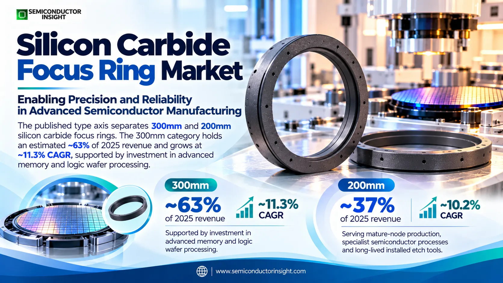
The published type axis separates 300mm and 200mm silicon carbide focus rings. The 300mm category holds an estimated ~63% of 2025 revenue and grows at ~11.3% CAGR, supported by investment in advanced memory and logic wafer processing. The 200mm category contributes ~37% with a growth outlook near ~10.2%, serving mature-node production, specialist semiconductor processes and long-lived installed etch tools.
| Wafer size | Technical function and installed tool base | Market position and replacement economics |
|---|---|---|
| 300mm | Rings for 300mm etch chambers surround a large wafer and help maintain a controlled plasma boundary near the perimeter. They are specified alongside chamber electrode geometry and electrostatic chuck dimensions, often for high-aspect-ratio etching in memory and advanced logic. Tight concentricity, surface condition and contamination control are important because the value of a processed 300mm wafer can be high and process windows narrow. | Largest type: estimated ~63% share in 2025, ~11.3% CAGR. The model assigns USD 78.1 million in 2025, USD 86.9 million in 2026 and USD 204.7 million in 2034 to this wafer format. High-throughput fabs consume replacement rings as part of preventive maintenance, and new etch chambers add initial demand. Qualification may be tool-specific even within the same nominal wafer diameter, so vendors compete through part repeatability, documented material purity and response times for urgent replacement rather than through commodity ceramic pricing alone. |
| 200mm | Rings designed for 200mm tools serve a varied installed base including power semiconductors, analog devices, sensors and specialty processes. Older chamber platforms may remain productive for many years, and suppliers must reproduce dimensions and material behaviour for equipment that is no longer at the centre of a manufacturer’s new product roadmap. Cleaning cycles and the chemistry of individual recipes determine replacement frequency. | Estimated ~37% share in 2025, ~10.2% CAGR. Modeled revenues are USD 45.9 million for 2025, USD 50.6 million for 2026 and USD 110.0 million for 2034. This format remains commercially relevant because mature fabs continue to operate and require consumable spares. Smaller batch sizes and a wider variety of chamber designs can increase manufacturing complexity for ring suppliers. Customers value reverse-engineering capability and consistent fit, particularly when an original equipment maker has discontinued a specific part number. |
Material performance and chamber-specific qualification
Both wafer diameters require resistance to reactive plasma, thermal shock and chemical attack, but a larger ring has different machining and flatness challenges. Silicon carbide can be produced using distinct processing routes, including chemical-vapour-deposited and recrystallised material forms, and the chosen grade must match the plasma chemistry. A supplier’s ability to meet contamination specifications can be more important than the nominal density or hardness of the material alone.
The Type axis refers to the wafer size served, not to the diameter of the ring’s outer edge. Each finished ring is larger than the wafer and its geometry is determined by the chamber interface. Product drawings therefore include inner and outer diameters, height, edge profiles and tolerances; no universal ring size is inferred merely from the 200mm or 300mm wafer label.
Segment Analysis: By Application
By application, the publisher distinguishes Wafer Etching and Others. Wafer Etching represents an estimated ~87% of 2025 revenue and expands near ~11.2% CAGR because edge rings are recurring consumables in plasma-based pattern transfer. The Others category holds ~13% and grows around ~8.8%, reflecting specialised process and engineering uses that do not fit the principal wafer-etching classification.
| Application | Demand characteristics |
|---|---|
| Wafer Etching | Dominant application: ~87% share, ~11.2% CAGR. Modeled values are USD 107.9 million in 2025, USD 120.0 million in 2026 and USD 280.5 million by 2034. Reactive-ion and other plasma etch processes use focus rings to manage the wafer-edge environment and reduce non-uniformity. Rings erode or accumulate process deposits and must be cleaned or replaced to maintain a stable recipe. High-aspect-ratio memory structures and advanced logic steps increase the sensitivity to edge effects, making dimensional repeatability and low particle shedding commercially important. |
| Others | Estimated ~13% share, ~8.8% CAGR. The model allocates USD 16.1 million to 2025, USD 17.5 million to 2026 and USD 34.4 million to 2034. The residual category includes specialised plasma-process setups, engineering evaluation and related chamber-edge applications that require silicon carbide rings but are not classified as mainstream wafer etching. Buyers may purchase lower quantities or customised geometries for laboratory and pilot equipment. The category is not a catch-all for complete deposition systems or other semiconductor consumables. |
The difference between applications is the intensity of repeated plasma exposure. A high-volume etch chamber may undergo frequent part changes because wear changes the boundary condition at the wafer edge, whereas an engineering chamber can retain a ring longer while running fewer wafers. Maintenance planners evaluate cost per usable wafer and downtime, not simply the purchase price of a ceramic component.
Demand is linked to the installed chamber population, recipe severity and utilisation. A new wafer fab can create initial ring orders, but the larger recurring business emerges after the tools reach production. Conversely, an equipment spending slowdown does not immediately eliminate replacement demand from operating fabs, giving the consumable market a different cycle from the market for new etch tools.
Regional Analysis
Asia-Pacific leads with an estimated ~49% of 2025 silicon carbide focus-ring sales and ~11.6% CAGR, followed by North America at ~24% and Europe at ~16%. South America contributes ~6%, while the Middle East & Africa accounts for ~5%. Demand depends on wafer fab installations and operating hours, and a ring sold into an Asian fab may have been manufactured by a supplier headquartered elsewhere.
Where are plasma etch consumables purchased and qualified?
The regional pattern follows wafer-processing capacity rather than the geography of finished chip consumption. Taiwan and South Korea host dense concentrations of advanced manufacturing, China continues to add domestic capacity, and Japan supports memory and specialty semiconductor production. The United States is expanding domestic fabrication while Europe retains important automotive and industrial semiconductor operations. Consumable qualification usually takes place with the fab or tool maker, so local technical support matters.
A focus ring is often purchased through an approved parts channel associated with an etch platform. Some customers source original equipment components, while others qualify specialist ceramics suppliers to reduce cost or improve lifetime. Where plasma conditions are especially demanding, replacement intervals can be short enough that local inventory has meaningful value. Smaller regions may import most rings, making distributor reliability and customs lead time relevant purchasing factors.
| Region | Position | Growth outlook | Demand profile | What decides supplier selection |
|---|---|---|---|---|
| Asia-Pacific | Largest (~49%); modeled 2025 USD 60.8m / 2034 USD 163.2m | Highest outlook (~11.6% CAGR) | 300mm logic and memory fabs; extensive etch tool utilisation | Process compatibility, purity and fast spare delivery |
| North America | Second (~24%); modeled 2025 USD 29.8m / 2034 USD 72.5m | Growth near ~10.4% CAGR | US advanced manufacturing and specialist process development | Tool qualification, traceability and domestic support |
| Europe | Third (~16%); modeled 2025 USD 19.8m / 2034 USD 46.8m | Steady expansion (~10.0% CAGR) | Industrial, automotive and specialty semiconductor fabs | Repeatable geometry and approved maintenance practices |
| South America | Emerging (~6%); modeled 2025 USD 7.4m / 2034 USD 17.8m | Growth near ~10.2% CAGR | Limited domestic wafer fabrication and technical services | Imported parts availability and local integrator relationships |
| Middle East & Africa | Developing (~5%); modeled 2025 USD 6.2m / 2034 USD 14.7m | Growth near ~10.1% CAGR | New semiconductor ecosystem initiatives and research tools | Procurement scale and specialised technical expertise |
Silicon Carbide Focus Ring Suppliers and Competitive Landscape
Focus-ring competition is specialised because customers require high-purity SiC materials, exact chamber geometry and stable plasma behaviour. The supplier landscape includes technical ceramics manufacturers, semiconductor equipment service companies and regional precision-machining firms. Product verification matters: a company that makes generic silicon carbide parts or complete etch tools is not automatically a qualified source of focus rings for a particular process.
CoorsTek and Kallex publish direct evidence of focus and edge rings used in plasma etch chambers. CoorsTek lists chemical-vapour-deposited silicon carbide among the materials it supplies for aggressive chamber environments, while Kallex highlights resistance to ion bombardment, corrosion and thermal deformation. These specifications indicate why procurement teams compare material processing and finishing capability, not just the ring’s dimensional drawing. Suppliers may need to reproduce an approved part’s surface condition over repeated production lots.
The publisher also lists Daewon, Greene Tweed, Tokai Carbon, Worldex, Max Luck Technology and Ferrotec. Their roles in technical ceramics, precision materials or semiconductor equipment supply can be relevant, but an individual product family should be verified before assigning a leadership tier. A broad company revenue figure cannot be substituted for focus-ring sales, and the company list does not provide evidence that each vendor has the same geographic coverage or manufacturing capacity.
Etch equipment manufacturers influence competition through chamber design and spare-part qualification. Lam Research has described replaceable edge-ring systems and control of wafer-edge effects, demonstrating that ring geometry is linked to process performance and maintenance strategy. A specialist replacement supplier can win business by extending component life or improving availability, but changing the part can alter plasma conditions and may require expensive requalification. This favours incumbents with proven process history.
The commercial value of a ring is measured partly in avoided downtime and wafer loss. A low-price component that sheds particles or erodes unevenly can increase scrap or maintenance costs, while an expensive ring may justify its price if it delivers stable performance over more wafers. Suppliers therefore compete through surface finish, high-purity materials, metrology, cleaning compatibility and lead times. Capacity alone does not guarantee customer acceptance in a contamination-sensitive fab.
Tier structure
| Tier | Companies | Basis of competition |
|---|---|---|
| Direct product evidence | CoorsTek; Kallex | Published focus-ring product information identifies plasma etch use, material durability and wafer-edge control. These companies provide directly observable market participation, although their exact shares and shipment volumes are not publicly established by the product pages. |
| Publisher-listed specialists | Daewon; Greene Tweed; Tokai Carbon; Worldex; Max Luck Technology; Ferrotec | Names are retained from the publisher company list for research coverage. Product-specific participation, material grade and chamber approvals require case-by-case verification before assigning any independent sales ranking. |
| Equipment ecosystem | Lam Research and Applied Materials as etch equipment developers | These companies shape chamber requirements and consumable qualification but are not counted as separate independent focus-ring manufacturers merely because their tools use edge components. Their evidence informs technology demand and maintenance economics. |
Key companies profiled
- Kallex
- Daewon
- CoorsTek
- Greene Tweed
- Tokai Carbon
- Worldex
- Max Luck Technology
- Ferrotec
Silicon Carbide Focus Ring Production and Replacement Capacity Analysis
Production combines SiC material processing, precision machining, surface finishing and contamination screening. Ring geometry is often tailored to a particular etch chamber, so the effective capacity of a supplier depends on its ability to reproduce qualified parts consistently rather than the gross tonnes of ceramic material it can manufacture. The installed base of process tools also determines the volume and timing of replacement demand.
Manufacturing begins with a silicon carbide material form chosen for plasma durability, thermal behaviour and impurity limits. Chemical-vapour-deposited SiC, recrystallised SiC and other engineered ceramic routes have different cost and process characteristics. The producer must then machine the ring’s inner edge, outer diameter, height and surface profile to tight tolerances. Because a finished part operates beside a wafer, small deviations can influence process conditions and may be unacceptable even when the ceramic meets a generic materials specification.
Finishing and cleaning are central quality steps. A ring may require controlled surface roughness, removal of machining residues and inspection for embedded particles before it can enter a semiconductor clean environment. Packaging must preserve that cleanliness during shipping and storage. The qualification burden is especially high for 300mm advanced process tools, where ring erosion can affect edge critical dimensions and the cost of an affected wafer is significant.
The recurring replacement cycle creates a production-planning problem distinct from the sale of new fab equipment. Customers may request emergency spares when chamber performance changes unexpectedly, while routine maintenance can be forecast from historical process hours. Suppliers that maintain an approved inventory near large fab clusters can reduce downtime, but they must manage the risk of holding custom ring geometries that cannot be sold to another customer.
Production capacity is geographically dispersed among ceramics specialists and tool-related supply networks. Taiwan, Japan, South Korea, China, Europe and the United States participate in the broader ecosystem, although a specific focus ring may cross borders before final use. Investment in metrology, contamination control and repeatable SiC processing can raise the usable output of qualified rings without a proportional increase in raw ceramic capacity. This distinction matters when evaluating supplier scale.
Silicon Carbide Focus Ring Market Dynamics: Drivers, Restraints and Opportunities
Demand is linked to plasma etch chamber utilisation, wafer fab capacity additions and the need for stable edge performance. The replacement nature of focus rings provides a recurring revenue stream, but longer-lasting parts and alternative chamber materials can limit unit demand. Market growth also depends on whether suppliers can qualify high-purity products at an acceptable cost and maintain inventory close to semiconductor manufacturing clusters.
MARKET DRIVERS
Drivers Impact Analysis*
| Market Drivers | Impact Rank | CAGR Contribution (%) | 2026–2028 | 2029–2031 | 2032–2034 |
|---|---|---|---|---|---|
| 300mm advanced logic and memory etch capacity | High | +5.20% | High | High | Medium |
| Recurring plasma-chamber consumable replacement | Medium-High | +3.30% | High | High | High |
| Tighter wafer-edge uniformity specifications | Medium | +2.40% | Medium | High | High |
| Fab diversification and regional new-builds | Low-Medium | +1.60% | High | Medium | Medium |
| Others (specialty etch and retrofit programmes) | Low | +1.20% | Medium | Medium | High |
Advanced 300mm manufacturing adds demanding edge-control steps
As logic and memory architectures become more complex, process engineers require consistent plasma conditions across a large wafer. Focus rings are one part of the chamber system that controls the boundary at the wafer perimeter. SEMI’s 2026 equipment outlook indicates continued investment in wafer fabrication, but only the share associated with installed and operating etch chambers can ultimately translate into ring orders. The demand mechanism is therefore capacity plus process intensity, not a direct percentage of total equipment spending.
Replacement demand persists after an etch tool is installed
An edge ring experiences repeated ion exposure, chemical attack and cleaning, so its geometry and surface condition change over time. Fabs replace parts according to preventive maintenance plans or process-performance indicators, generating sales independent of new tool shipments. Lam Research’s automated ring exchange technology illustrates how important replacement time can be to production economics. The business opportunity lies in supplying approved spares reliably and managing inventory across chamber generations.
Stricter edge uniformity makes ceramic performance more valuable
At advanced process nodes, a small change in edge plasma distribution can affect critical dimensions or create particles that reduce usable wafer output. CoorsTek and Kallex both emphasise plasma resistance and material purity, indicating that suppliers must address more than basic mechanical fit. As process margins narrow, customers may accept a higher component price for better stability, provided the benefit is demonstrated through wafer-level qualification rather than assumed from a material datasheet.
Geographic diversification expands qualified spare networks
New semiconductor manufacturing sites require local service and supply chains for etch consumables. A ring supplier that can qualify with a tool maker and support fabs in multiple regions may gain business as equipment installations spread beyond traditional clusters. However, the qualification remains specific to chamber designs and process recipes, so geographic expansion does not mean a single standard ring can serve all new facilities.
Mature-node tools create a long-tail replacement business
Not every etch chamber processes 300mm wafers or uses the newest process architecture. Established 200mm fabs continue producing analog, power and specialty devices, and many older tools require replacement parts that are no longer widely stocked. A ceramics company with flexible machining and engineering support can serve these smaller programmes, although production runs may be short and inventory management more difficult than in a large advanced-memory fab.
MARKET RESTRAINTS
Restraints Impact Analysis*
| Market Restraints | Impact Rank | CAGR Contribution (%) | 2026–2028 | 2029–2031 | 2032–2034 |
|---|---|---|---|---|---|
| High-purity SiC material and machining cost | High | -1.00% | High | Medium | Medium |
| Long qualification and chamber compatibility cycles | Medium-High | -0.80% | High | Medium | Low |
| Longer-life components reducing replacement frequency | Medium | -0.60% | Medium | High | High |
| Others (alternative ceramics and fab utilisation swings) | Low | -0.40% | Medium | Medium | High |
Specialised production keeps costs above commodity ceramics
High-purity silicon carbide materials, precise machining and contamination-controlled finishing require equipment and expertise not needed for general industrial ceramic parts. Small custom orders can be expensive because setup, inspection and cleaning costs are spread over fewer units. Customers may still pay for reliable performance, but price pressure intensifies where multiple suppliers have qualified equivalent rings for a mature chamber platform.
Part qualification can delay a supplier change
A focus ring is part of the plasma process environment, so replacing an approved component can alter edge uniformity, particle generation or maintenance intervals. Fabs often need test wafers and process monitoring before accepting a new supplier. This creates a barrier for entrants and slows conversion from prototype samples to recurring orders, particularly in advanced 300mm manufacturing where yield sensitivity is high.
Improved ring lifetime can reduce the number of replacements
More durable SiC grades and better chamber cleaning procedures may extend the service life of a ring. That benefits fab productivity and can raise the value of an individual part, but it also means fewer replacement units per chamber over a fixed period. Suppliers must balance premium pricing against the possibility that a successful durability improvement reduces the frequency of future consumable orders.
Alternative materials and changing utilisation affect purchases
Alumina, quartz, silicon and coated ceramics may be selected for some plasma processes depending on chemistry and electrical requirements. Silicon carbide is not the optimal material in every chamber location, and tool makers may redesign parts as recipes change. In addition, a fab running below normal utilisation consumes fewer wear parts, so cyclical changes in semiconductor production can affect short-term demand even when installed equipment capacity remains unchanged.
MARKET OPPORTUNITIES
Longer-life qualified rings with measurable wafer-yield benefits
A supplier that documents lower particle generation or more stable etch uniformity over a full maintenance interval can justify a premium beyond the cost of raw silicon carbide. The strongest opportunity is in high-value 300mm processes where a small improvement in usable wafers outweighs the price of a consumable. Qualification data must be generated on the customer’s relevant plasma recipe to be commercially persuasive.
Automated replacement and predictive maintenance supply models
Lam Research has demonstrated automated exchange of edge rings without opening the chamber, creating an operating model in which consumables are stocked and changed through planned equipment routines. Ring suppliers may participate by providing tightly controlled dimensions, packaging and inventory logistics compatible with automated handling. This shifts competition toward reliability of supply and consistency across lots, not merely the performance of an isolated ceramic sample.
Specialist 200mm spares for mature and discontinued tools
Older plasma chambers remain productive in analog, power and sensor fabrication, yet exact replacement geometries can be difficult to source. Precision ceramics manufacturers able to reproduce qualified parts and maintain low-volume inventory can serve this long tail. The opportunity is particularly relevant when the original tool maker no longer promotes a part, although customers still require evidence that a substitute will not alter the validated process.
Regional inventory hubs near major wafer fab clusters
Focus-ring demand is concentrated near semiconductor fabs, and a delay in receiving a critical spare can extend equipment downtime. Suppliers can differentiate through local stock, cleaning and inspection capability, and rapid technical response. Establishing a regional hub requires knowledge of the installed chamber population, because the same nominal 300mm category contains many incompatible ring designs and stocking the wrong geometry creates costly inventory.
Silicon Carbide Focus Ring Supply Chain and Value Chain Analysis
The value chain begins with SiC ceramic material production, continues through precision shaping and contamination-controlled finishing, and ends with qualification and replacement inside plasma etch tools. Tool makers and fabs influence specifications, while specialist ceramics suppliers control material consistency and machining. The ring is a consumable whose commercial value depends on process uptime and wafer yield rather than the volume of raw silicon carbide sold.
Upstream. Material producers supply silicon carbide forms selected for plasma resistance and impurity limits. Different grades can respond differently to etch gases and RF environments, so a generic SiC specification is insufficient to establish chamber suitability. Upstream supply continuity matters because a change in raw material may require a new qualification cycle even if the finished ring dimensions remain unchanged. Raw ceramic revenue is an input cost, not an additional sale of the finished focus ring.
Manufacturing. Ring production requires accurate inner and outer profiles, stable flatness, controlled roughness and inspection for embedded contamination. Cleaning and packaging preserve the surface condition until installation in the chamber. The quality of these steps affects both initial plasma behaviour and the rate at which the ring erodes. A supplier can improve its competitive position by demonstrating repeatability across production batches rather than relying solely on an attractive material datasheet.
Channels. Some consumables reach fabs through equipment maker spare-parts programmes, while others are purchased from qualified independent ceramics specialists. Inventory planning is important because an unexpected ring failure can take a productive etch chamber offline. A supplier close to a major fab cluster can offer faster delivery, but it must stock the correct part revision and document traceability to avoid introducing an unapproved component into a sensitive process.
Downstream. Wafer fabs consume rings as part of plasma chamber maintenance and process control. The purchase decision may involve process engineers, maintenance teams, procurement and quality specialists because the part affects yield, uptime and contamination. Customers monitor replacement intervals and wafer results to judge whether a more durable or lower-cost ring provides genuine savings. This end-use structure creates repeat business after qualification but makes entry difficult for unproven suppliers.
Recent Developments in the Silicon Carbide Focus Ring Market
- 14 July 2026 Forecast
SEMI released its midyear semiconductor equipment outlook, forecasting USD 165.9 billion of total new equipment sales in 2026, a 23.2% increase, including USD 143.9 billion in wafer fab equipment after USD 116.9 billion in 2025; its 2028 total equipment projection was USD 229.5 billion. More etch capacity can eventually increase the installed population of chambers requiring focus rings, although the equipment forecast covers many tool types. It is used here as an adjacent demand signal, not as a direct estimate of ring sales. Source - 4 May 2026 Reported
The Semiconductor Industry Association reported first-quarter 2026 global semiconductor sales of USD 298.5 billion, up 25% from the preceding quarter. Strong chip demand can support fab utilisation and thus the consumption of plasma chamber spares. The sales total covers finished semiconductors across many applications and cannot be substituted for the revenue of a specific ceramic consumable. Source - 14 February 2025 Showcased
Kallex published a SiC edge focus-ring product update, reinforcing its offering of precision ceramic parts for semiconductor processing. The supplier’s product information emphasises plasma resistance and the ability to customise component geometry. The announcement is a product-availability instance rather than evidence of a particular shipment volume or global market-share ranking. Source - 8 October 2025 Forecast
SEMI issued a 300mm fab equipment outlook covering 2026–2028 investment of USD 94 billion in China, USD 86 billion in South Korea, USD 75 billion in Taiwan, USD 60 billion in the Americas, USD 32 billion in Japan, USD 14 billion in Europe and the Middle East, and USD 12 billion in Southeast Asia. The forecast illustrates the geographic concentration of advanced wafer processing that underpins ring consumption. Its monetary totals concern fab equipment investment, so only the qualitative connection to installed plasma etch capacity is used in the consumables market analysis. Source - 24 April 2019 Introduced
Lam Research described its Corvus R automated edge-ring exchange system for plasma etch tools, allowing worn rings to be replaced without opening the chamber. The technology illustrates the importance of consumable change-out time and process stability in semiconductor manufacturing. Automated handling creates demand for repeatable ring dimensions and controlled inventory even as maintenance procedures become more efficient. Source
REPORT SCOPE & SEGMENTATION
| Attribute | Details |
|---|---|
| Study Period | 2020–2034 |
| Base Year | 2025 |
| Estimated Year | 2026 |
| Forecast Period | 2026–2034 |
| Historical Period | 2020–2024 |
| Market Size 2025 | USD 124 million |
| Market Size 2026 | USD 138 million |
| Market Size 2034 | USD 315 million |
| Growth Rate | CAGR of 10.9% from 2026–2034 |
| Unit | Value (USD Million); segment and regional shares are estimates |
| Segmentation | By Type, By Application and By Region |
| By Type | 300mm · 200mm |
| By Application | Wafer Etching · Others |
| By Region | Five-region demand analysis by wafer diameter, application, fab location and replacement channel North AmericaUnited States, Canada, Mexico EuropeGermany, France, Italy, United Kingdom, Rest of Europe Asia-PacificTaiwan, South Korea, China, Japan, India, Southeast Asia, Rest of Asia-Pacific South AmericaBrazil, Argentina, Chile, Rest of South America Middle East & AfricaIsrael, Saudi Arabia, UAE, South Africa, Rest of Middle East & Africa |
| Key Companies Profiled | Kallex; Daewon; CoorsTek; Greene Tweed; Tokai Carbon; Worldex; Max Luck Technology; Ferrotec |
| Customization Scope | Free report customization (equivalent to up to 4 analyst working days) with purchase. Country-level wafer fab mapping and ring material specifications can be added within an agreed research scope. |
Frequently Asked Questions
What is the size of the global silicon carbide focus ring market?
The worldwide focus-ring market registered USD 124 million in 2025 and is forecast to reach USD 315 million by 2034, at a CAGR of 10.9% over 2026–2034. Growth reflects plasma etch chamber additions and recurring replacement of edge components as semiconductor fabs run production wafers. Ring revenue is distinct from the value of etch tools and finished chips.
What does a silicon carbide focus ring do in a plasma etch chamber?
A focus ring surrounds the wafer edge and helps maintain the electric-field and plasma conditions required for uniform etching. It is made from a material that withstands energetic ions, reactive gases and repeated cleaning. As the surface erodes, the part may need replacement to prevent changes in edge processing or particle contamination. It is therefore both a process-control component and a recurring maintenance consumable.
Which companies supply silicon carbide focus rings?
The profiled supplier list includes Kallex, Daewon, CoorsTek, Greene Tweed, Tokai Carbon, Worldex, Max Luck Technology and Ferrotec. CoorsTek and Kallex provide directly identifiable focus-ring product information, while other listed names require product-level verification before a numerical market rank can be assigned. Etch equipment manufacturers also influence component qualification, but their entire equipment revenue is not part of ring sales.
Which wafer diameter accounts for the largest focus-ring share?
The 300mm type is the leading category at an estimated ~63% of 2025 revenue, while 200mm contributes about ~37%. Advanced memory and logic fabs commonly use 300mm processing, generating demand for large, highly qualified rings. Older and specialty fabs maintain 200mm equipment that still consumes spares, so smaller-wafer rings remain commercially relevant despite the investment emphasis on advanced manufacturing.
What is the largest application for silicon carbide focus rings?
Wafer Etching accounts for an estimated ~87% of 2025 demand and grows at roughly ~11.2% CAGR. Plasma etch processes expose edge rings to aggressive conditions that can change their geometry and surface cleanliness over time. The remaining ~13% belongs to specialised process and engineering uses, not to all other silicon carbide components or the complete value of semiconductor fabrication equipment.
Which region leads the silicon carbide focus ring market?
Asia-Pacific leads with an estimated ~49% of 2025 revenue and the strongest projected growth near ~11.6% CAGR. North America follows at ~24%, Europe ~16%, South America ~6% and the Middle East & Africa ~5%. The geographic model reflects where wafer etch chambers operate and consume replacement rings rather than the home country of a ceramic supplier or the destination of finished electronic products.
Why do focus rings require regular replacement?
Plasma ions, reactive chemicals and cleaning processes progressively wear or modify a ring’s surface. Even when the part remains mechanically intact, changes in edge geometry or contamination can alter wafer processing results. Fabs therefore schedule maintenance or replace rings after observing process drift. The exact interval depends on recipe chemistry, chamber power, cleaning practice and wafer throughput rather than a universal number of operating hours.
What are the main barriers for a new focus-ring supplier?
The central obstacles are high-purity material processing, precise machining and customer qualification. A replacement part must fit the chamber and produce stable plasma behaviour without introducing particles, and approval may require test wafers and process monitoring. Small production runs can be expensive because cleaning, metrology and documentation costs remain high. Suppliers also need dependable delivery for customers that cannot tolerate extended etch-tool downtime.
How does 300mm fab expansion affect ring demand?
New 300mm fabs and etch tools create initial orders for qualified chamber components, then ongoing replacement demand once production begins. Investment forecasts from SEMI help identify regions where the installed tool base may expand, but they include many types of equipment beyond plasma etching. Ring sales depend on actual chamber installation, utilisation and maintenance intervals, so a fab investment dollar cannot be converted directly into focus-ring revenue.
What is included in the focus-ring market study?
The study covers finished silicon carbide focus and edge rings used in semiconductor processing, segmented by 300mm and 200mm wafer formats and by Wafer Etching and Others applications. It evaluates five regional markets, the 2025 base year and the 2026–2034 forecast period. Complete etch equipment, other chamber ceramics, raw SiC wafers and semiconductor device sales are outside the finished-ring revenue boundary.
Research Sources & Evidence Base
Get Sample Report PDF for Exclusive Insights
Report Sample Includes
- Table of Contents
- List of Tables & Figures
- Charts, Research Methodology, and more...
 Download Sample Report PDF