Key Takeaways
- 2025 device-component value: The global market for fabricated silicon-carbide rings reached USD 124 million, covering precision annular components rather than semiconductor chip sales or complete processing equipment.
- Long-term expansion: The market is projected to reach USD 315 million by 2034 at a 10.9% CAGR over 2026–2034, reflecting rising demand for plasma-resistant consumables.
- Leading diameter class: The 300mm class commands an estimated ~65% of 2025 value, while 200mm products contribute ~35% through established and specialty wafer-processing lines.
- Primary application: Wafer Etching accounts for an estimated ~76% of ring revenue; Others (~24%) includes compatible deposition and non-etch process positions where qualified SiC rings are used.
- Regional concentration: Asia-Pacific leads at an estimated ~51% of sales, followed by North America (~25%), Europe (~18%), South America (~4%) and Middle East & Africa (~2%).
SiC Ring Market Overview
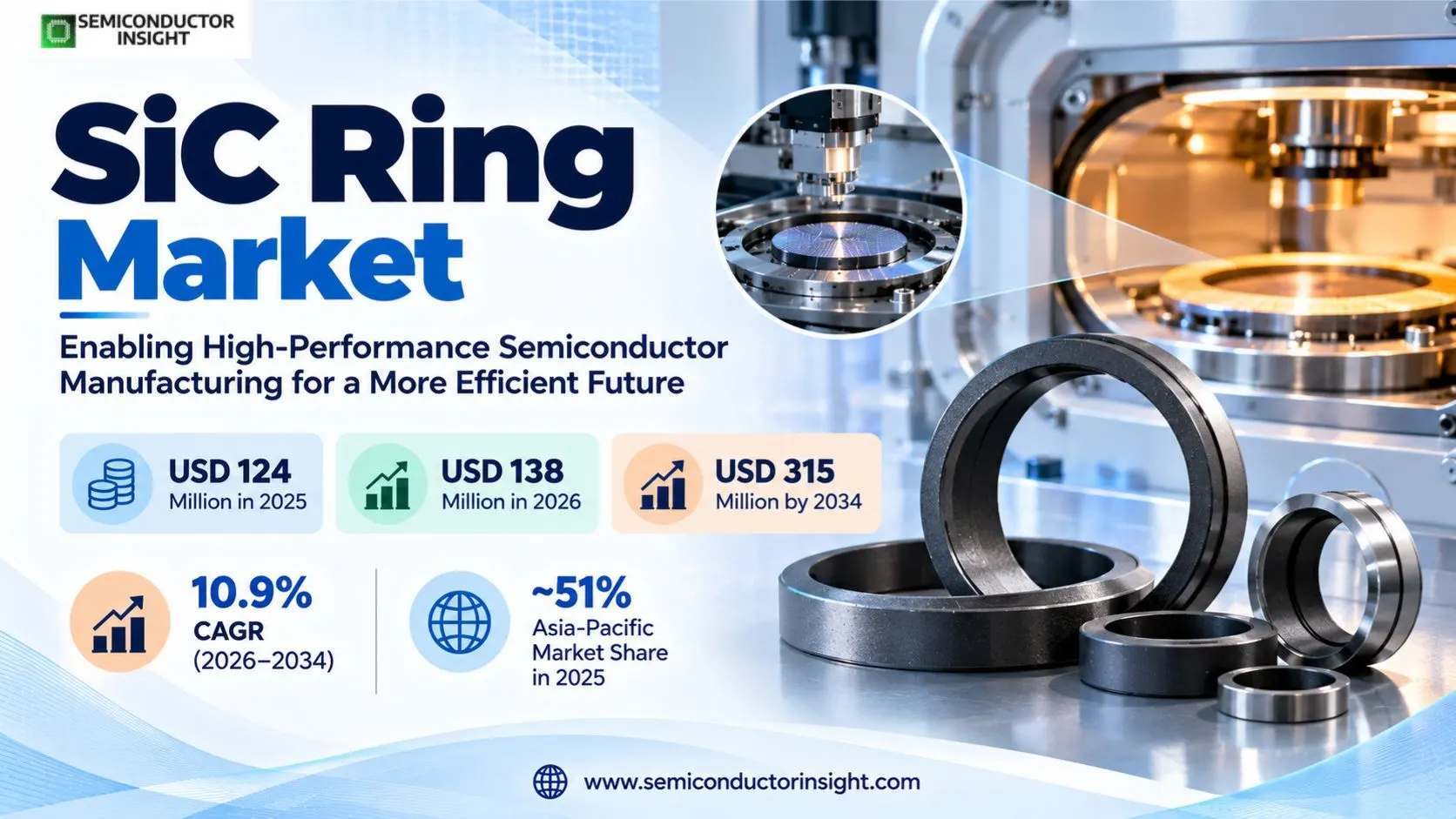
SiC ring market was valued at USD 124 million in 2025, is estimated at USD 138 million in 2026 and is forecast to reach USD 315 million by 2034, representing a 10.9% CAGR during 2026–2034. Asia-Pacific leads with an estimated ~51% share as advanced wafer-processing equipment requires durable, low-contamination chamber consumables.
Base year: 2025 | Estimated year: 2026 | Forecast year: 2034 | USD million | Type: 300mm, 200mm | Application: Wafer Etching, Others
Silicon-carbide rings are engineered annular parts placed around wafers or in compatible high-temperature processing positions, where plasma exposure, reactive gases and repeated chamber cleaning degrade less-resistant materials. Their commercial value comes from dimensional accuracy, controlled surface purity and service life rather than from their use as active electrical switches. In a 300mm etch chamber, a focus or edge ring helps control processing conditions near the wafer perimeter, making replacement-part quality relevant to yield and maintenance planning.
Demand rises with the installed base and utilization of plasma etch tools, not simply with worldwide chip revenue. A high-volume fabrication plant may replace chamber rings according to accumulated process exposure, while a research line purchases fewer parts but requires specialized geometries. SEMI projected expanding 300mm fabrication-equipment investment during 2026, providing adjacent evidence of capacity development. Those capital-expenditure figures cannot be added to the ring market, which covers a much narrower class of consumable components.
The market includes two diameter classes corresponding to common equipment families: 300mm rings lead at an estimated ~65% of 2025 revenue, and 200mm parts represent ~35%. The higher-value 300mm category reflects advanced logic and memory manufacturing, demanding tolerances and repeated plasma processing steps. Smaller-format equipment remains important for mature technologies, specialty devices and replacement demand, with procurement shaped by legacy chamber dimensions and supplier support rather than a universal transition to larger wafers.
Wafer Etching is the dominant application at an estimated ~76% of component sales because focus and edge rings help manage plasma uniformity and wafer-edge exposure. The remaining ~24% is associated with other qualified chamber and industrial ring applications described within the product category, including selected deposition or high-wear positions. SiC-coated graphite and bulk CVD SiC have different cost, purity and durability profiles, and customers assess particle generation and chemical resistance under specific process recipes before choosing a construction method.
Asia-Pacific accounts for an estimated ~51% of global value, reflecting its concentration of semiconductor fabrication capacity and ceramic-component manufacturing. North America holds ~25%, Europe ~18%, South America ~4% and Middle East & Africa ~2%, with smaller markets often buying through equipment service providers. The outlook depends on fab construction, installed tool utilization, ring replacement frequency and material qualification; it does not assume that silicon-carbide rings are standard parts inside electric-vehicle traction inverters or finished power transistors.
Segment Analysis: By Type
Diameter is the central product classification because the chamber, electrostatic chuck and wafer-edge geometry determine whether a ring can be installed. The 300mm class leads with an estimated ~65% of 2025 revenue and a modeled ~12.0% annual growth path, while 200mm parts hold ~35% with ~8.5% growth. The two classes are not interchangeable: each requires process-specific tolerances, plasma compatibility and maintenance qualification.
| Country | Position in region | What drives demand |
|---|---|---|
| China | Expanding chamber installed base | Chinese wafer-fab investment supports purchases of 300mm chamber parts as well as replacement rings for established 200mm lines. Procurement may favour local machining and material suppliers when they can demonstrate low particle generation and stable etch performance. The technical challenge is qualifying ring geometry against tool-specific plasma recipes, since a nominal diameter match does not guarantee acceptable edge uniformity or long service life. |
| Type | Function | Market position |
|---|---|---|
| 300mm | The 300mm ring class supports larger-diameter wafer processing, especially in advanced logic and memory fabs that use multiple plasma etch steps. Components must align with the wafer perimeter, electrostatic chuck and chamber hardware, and a minor dimensional mismatch can affect edge uniformity or particle behaviour. Dense CVD SiC and carefully controlled coatings help withstand aggressive halogen chemistry and repeated cleaning. Purchasers validate each design for specific tools rather than ordering solely by nominal diameter. | Largest type at an estimated ~65% of 2025 market revenue and modeled ~12.0% annual growth, driven by advanced-wafer tool installations and consumable replacement. The value proposition combines erosion resistance, contamination control and repeatable precision machining, while production yields depend on material density and finishing quality. Ring vendors can strengthen customer retention through qualified replacement programmes, although high-purity fabrication costs and longer validation cycles limit how quickly new suppliers enter established chambers. |
| 200mm | The 200mm category serves mature-node fabrication, specialty electronics, power devices and research processes where smaller wafer platforms remain economically viable. Equipment fleets can remain in service for many years, creating recurring demand for rings matched to legacy chamber dimensions. Suppliers must reproduce geometry and surface characteristics consistently, because a ring that fits mechanically may still alter plasma distribution or introduce particles. Service availability and dependable replacement lead times are therefore central to the customer relationship. | The 200mm class accounts for an estimated ~35% of 2025 sales and grows at a modeled ~8.5% rate, reflecting mature fabrication lines and specialty equipment. Revenue is supported by consumable wear and maintenance rather than wholesale replacement of every existing tool. Smaller orders can be technically demanding, and suppliers that preserve drawings and process history can serve long-life equipment profitably even as the newest advanced-node investments favour 300mm wafer processing. |
300mm rings for advanced wafer chambers
Larger wafers increase the economic consequences of edge nonuniformity because one poorly controlled process step can affect many die locations. A 300mm SiC ring must withstand plasma bombardment and remain dimensionally stable while nearby parts cycle between cleaning and deposition conditions. Fabricators therefore assess porosity, trace impurities, surface finish and reproducibility. Ring qualification can require multiple process runs, making an approved consumable difficult to replace purely on price.
The 2026–2034 outlook for 300mm components reflects additional etch chambers as well as higher utilization of existing tools. A 300mm fab equipment forecast is only an indirect demand indicator: the ring purchase depends on the actual chamber design and maintenance schedule. Manufacturers able to machine complex geometries and maintain CVD material purity can compete for higher-value replacement contracts, while low-cost alternatives face stringent particle and lifetime tests.
200mm rings in mature and specialty fabrication
A 200mm plasma chamber may continue producing power, analog or specialty devices long after newer leading-edge fabs have standardized larger substrates. Operators still need replacement focus rings that match existing tool interfaces and established process recipes. Because production volumes vary, small-batch machining and stocked spare parts become important commercial services. High-purity SiC remains useful where corrosive gases or cleaning cycles would otherwise accelerate wear.
Demand for 200mm rings is less dependent on new advanced-node capacity and more connected to utilization, refurbishment and the installed equipment base. A customer replacing a worn ring seeks stable etch performance with minimal retuning, so documentation of geometry and material grade has measurable value. Suppliers can maintain recurring revenue through aftermarket channels, although price sensitivity and equipment obsolescence constrain the growth trajectory.
Segment Analysis: By Application
The application split is led by Wafer Etching at an estimated ~76% of 2025 revenue and a modeled ~11.5% growth rate. Others accounts for ~24% with ~8.9% modeled growth and captures compatible process-chamber and industrial ring uses outside the dominant etch position. Ring purchasing is tied to component wear, contamination risk and qualified equipment recipes, so the same material grade may not perform identically in etching and deposition environments.
| Application | Demand characteristics |
|---|---|
| Wafer Etching | Wafer Etching represents an estimated ~76% of SiC ring value because plasma exposure erodes parts around the wafer edge and can change process uniformity over time. A focus ring is selected for its interaction with the electrostatic chuck, RF field and chamber chemistry, not just its nominal 300mm or 200mm diameter. Suppliers must control particles, impurities and geometry through repeated replacement cycles. The modeled ~11.5% growth rate reflects rising etch intensity and fab utilization, with service intervals varying by process recipe. |
| Others | Other applications account for an estimated ~24% of 2025 ring revenue and follow a modeled ~8.9% growth path. These uses include compatible CVD and PECVD chamber positions, selected high-temperature process fixtures and specialized wear-resistant annular parts within the product definition. Qualification is highly application-specific: a ring exposed mainly to heat can require different coating thickness or thermal expansion behaviour from one facing energetic plasma. Smaller markets value customization and reliable maintenance support but cannot be treated as equivalent to the full semiconductor equipment market. |
In etch chambers, the economic cost of contamination can outweigh the price of the consumable, especially when a failed edge component forces additional cleaning or rework. A 300mm ring with stable plasma resistance can protect process consistency over repeated tool cycles, while the operator still needs a planned replacement schedule. Outside etching, customers may place more emphasis on chemical compatibility or thermal stability, making material construction and surface treatment key segmentation factors.
The broad product category also encompasses industrial SiC ring components where the publisher includes them, but semiconductor demand should not be inferred from every automotive or renewable-energy equipment announcement. A mechanical seal ring in a chemical pump and a plasma focus ring have distinct specifications and buyers. The Wafer Etching versus Others allocation therefore separates dominant semiconductor chamber consumption from secondary ring uses without adding the selling value of the machines in which they operate.
Regional Analysis
The regional mix places Asia-Pacific first with an estimated ~51% of 2025 SiC ring revenue and modeled ~11.8% annual growth. North America follows at ~25% and ~10.3% growth, while Europe holds ~18% and ~10.4% growth. South America (~4%, ~9.0%) and Middle East & Africa (~2%, ~8.0%) rely more heavily on imported chamber consumables and specialized industrial ring demand than on large domestic advanced-wafer fab networks.
How do fab geography and chamber maintenance affect regional ring sales?
Ring demand is a function of where plasma processing takes place, how intensively tools operate and which component manufacturers have qualified for the chamber designs in service. Asia-Pacific combines extensive fabrication capacity with regional suppliers of advanced ceramics, whereas North America buys substantial high-purity consumables for logic, memory and specialty processing. European fabs emphasize long equipment life and rigorous contamination controls. The smaller regions typically purchase through imported tool-service arrangements and industrial distribution channels.
The regional estimates are not allocations of global semiconductor sales or wafer-fab equipment spending. Those larger markets provide context for chamber installation and utilization but cannot establish a precise ring-revenue denominator. A 300mm memory fab may consume numerous replacement rings over its life, while a smaller 200mm specialty facility could retain a stable installed fleet for years. Supplier geography also differs from sales destination, because a ring manufactured in Asia may be installed in a North American or European chamber.
| Region | Position | Growth outlook | Demand profile | What decides supplier selection |
|---|---|---|---|---|
| Asia-Pacific | Largest (~51%) | Highest (~11.8% CAGR) | Large advanced-wafer fabrication base | Chamber qualification, cost and high-purity machining |
| North America | Second (~25%) | Moderate (~10.3% CAGR) | Logic, memory and specialty fabs | Particle control, supplier traceability and service support |
| Europe | Third (~18%) | Steady (~10.4% CAGR) | Industrial and specialist wafer processes | Long-life tooling, precision and chemical compatibility |
| South America | Fourth (~4%) | Developing (~9.0% CAGR) | Imported equipment and industrial rings | Distributor stock, landed cost and maintenance support |
| Middle East & Africa | Fifth (~2%) | Selective (~8.0% CAGR) | New fab projects and industrial wear parts | Project qualification and local service arrangements |
Why does Asia-Pacific lead demand for SiC rings?
Asia-Pacific represents an estimated ~51% of 2025 global SiC ring revenue, supported by dense wafer-fabrication clusters and manufacturers of CVD SiC and precision ceramic components. China, Taiwan, South Korea and Japan use substantial 300mm processing capacity, while 200mm tools remain active in specialty production. The modeled ~11.8% growth rate reflects increasing etch intensity and component replacement, with suppliers competing on purity, delivery reliability and qualification to specific chamber geometries.
| Country | Position in region | What drives demand |
|---|---|---|
| China | Expanding chamber installed base | Chinese wafer-fab investment supports purchases of 300mm chamber parts as well as replacement rings for established 200mm lines. Procurement may favour local machining and material suppliers when they can demonstrate low particle generation and stable etch performance. The technical challenge is qualifying ring geometry against tool-specific plasma recipes, since a nominal diameter match does not guarantee acceptable edge uniformity or long service life. |
| Argentina | Specialized industrial applications | Argentina’s ring demand is concentrated in process industries and small specialist equipment markets where corrosion and abrasion resistance justify engineered ceramic components. High-purity semiconductor focus rings form a narrower opportunity than in regions with large wafer-fab clusters. Buyers often request replacement parts compatible with existing machinery and may accept longer lead times for custom dimensions. Currency and procurement constraints can make total landed cost decisive even when SiC offers longer service life. |
| Chile | Harsh-duty industrial equipment | Chilean mining and chemical-processing equipment can create opportunities for durable SiC rings where pumps or rotating assemblies encounter abrasive materials and corrosive fluids. These applications differ from 300mm wafer etching and should be treated as separate end-use demand within the broad ring category. Customers prioritize mechanical durability, field repairability and replacement stock, while semiconductor-grade particle specifications are only relevant when the component actually enters a cleanroom process. |
Market instances
- Import-led maintenance drives component purchases. A South American facility operating a specialized plasma or industrial process tool may need a custom SiC ring long after the original equipment was installed. The order can be small in volume but high in engineering importance because geometry and material compatibility must match the existing process. This supports distributor-led replacement business without implying that the region has the same advanced-wafer fabrication intensity as East Asia.
- Industrial wear duties create a distinct buying logic. In corrosive pumping or abrasive equipment, a SiC ring can be evaluated for resistance to wear and chemical attack rather than plasma-uniformity control. The supplier may provide a mechanically matched component with different purity requirements from a semiconductor focus ring. This application broadens the ring revenue boundary only when the product is actually an annular SiC part, and it must not be confused with the total value of the pump.
What limits SiC ring scale in Middle East and Africa?
Middle East & Africa contributes an estimated ~2% of 2025 SiC ring revenue and follows a modeled ~8.0% annual growth trajectory. Semiconductor process-chamber demand remains project-specific, while industrial rings can serve petrochemical, utility and other high-wear equipment. The Gulf states may import advanced fabrication tools or ceramic parts for industrial installations, and South Africa has specialist manufacturing and process-industry demand. Customers rely on qualified overseas suppliers and service partners for custom dimensions and replacement continuity.
| Country | Position in region | What drives demand |
|---|---|---|
| Saudi Arabia | Industrial process demand | Saudi Arabia has process industries where abrasion, corrosion and high operating temperatures can justify SiC rings in mechanical equipment. Semiconductor chamber rings represent a separate, more limited category tied to actual cleanroom installations. International vendors typically supply precision ceramic parts through equipment manufacturers or specialized distributors. Customers assess component lifetime, compatibility with aggressive fluids and the availability of replacements, rather than treating national industrial investment as direct ring sales. |
| United Arab Emirates | Equipment and distribution hub | The United Arab Emirates functions as an import and engineering-service hub for industrial equipment and selected high-technology installations. SiC ring demand can arise from maintenance of corrosive-process machinery or specialized fabrication systems, with procurement routed through regional integrators. A 200mm or 300mm semiconductor focus ring needs cleanroom-compatible qualification, whereas a wear ring in a pump follows mechanical performance criteria. Distributors must distinguish these requirements when supplying parts. |
| South Africa | Mining and chemical-processing uses | South African mines and chemical plants use equipment exposed to abrasive slurries and demanding fluids, creating potential demand for durable SiC annular components. Local semiconductor etch-ring consumption is much smaller than in leading wafer-fabrication regions, and the two applications require different purity and geometry controls. Industrial buyers prioritize replacement lead time, seal compatibility and field service, which can favour established distributors with access to specialized ceramic machining. |
Market instances
- Industrial chemical resistance supports niche demand. A petrochemical facility replacing an eroded seal ring may select SiC because it offers useful hardness and chemical resistance under demanding operating conditions. The component is evaluated as part of a mechanical assembly, not as a wafer-edge plasma control element. This supports a modest regional opportunity for specialty ring suppliers, with orders influenced by maintenance schedules and the ability to match installed equipment dimensions.
- Project timing shapes high-purity chamber orders. A new semiconductor or research installation in the Gulf may require 200mm or 300mm chamber consumables, but ring purchases normally follow tool delivery, process qualification and routine operation. Announced facility investment does not translate immediately into SiC component revenue. Vendors that can support commissioning and provide qualified spare parts are better positioned than suppliers relying solely on catalogued material properties or general industrial distribution.
Competitive Landscape of SiC Ring Manufacturers
The SiC ring supply chain combines high-purity ceramic producers, CVD materials specialists, precision machinists and equipment-approved component vendors. CoorsTek and Ferrotec provide direct technical evidence for semiconductor process components, while Kallex, Daewon, Tokai Carbon, Worldex, Max Luck Technology and Greene Tweed appear in the historical competitive set. Supplier positioning depends on qualified 200mm and 300mm ring geometries, trace impurities, plasma durability and reliable aftermarket delivery rather than headline chip production alone.
CoorsTek documents focus and edge rings among its plasma-etch ceramic products and offers several material options, including CVD SiC. Ferrotec describes CVD silicon-carbide processing and semiconductor-equipment applications, demonstrating a different manufacturing route and regional supply footprint. Smaller specialists can compete by machining complex annular shapes and reproducing tight tolerances, but entry into an established chamber often requires lengthy process testing. A low-priced unqualified replacement may cost more than its savings if it increases particles or wafer-edge defects.
Product construction creates meaningful competition. Bulk CVD SiC can offer high density and purity, whereas coated graphite or alternative ceramic substrates may provide different thermal, electrical and cost characteristics. Semicorex and Semicera describe CVD SiC etching rings, and Entegris supplies related high-purity SiC material and coating technologies. These product examples should not be collapsed into a single supplier ranking because some firms sell rings, others supply coatings or adjacent process parts, and still others participate upstream in SiC materials.
Customers tend to qualify components at the chamber and recipe level, limiting rapid switching between suppliers even when several manufacturers can machine a 300mm ring. Quality audits can examine trace metals, porosity, surface roughness and erosion behaviour under fluorine or chlorine plasma. The replacement business rewards consistent manufacturing lots and timely field support. Suppliers serving 200mm legacy tools may have smaller order quantities but long customer relationships based on preserved specifications and repeatable performance.
The historical company list includes businesses with varying current product disclosures. Tokai Carbon has documented SiC material capabilities through a 2024 polycrystalline substrate partnership, but that agreement is not evidence of ring sales. Greene Tweed is active in advanced sealing and materials, yet a named company should not be described as a leading SiC focus-ring seller without product-level support. Competitive analysis therefore distinguishes directly documented ring offerings from adjacent technical capabilities and legacy market labels.
Tier structure
| Tier | Companies | Basis of competition |
|---|---|---|
| Documented chamber suppliers | CoorsTek, Ferrotec, Semicorex, Semicera | These manufacturers provide public technical descriptions of plasma-facing SiC or CVD SiC components, including focus or etching rings and related process parts. Their products address high-purity, corrosion resistance and geometry requirements that matter in 200mm and 300mm chambers. Customers still need to verify exact tool compatibility and qualification status, so direct product evidence is not the same as an audited share of the global ring market. |
| Specialist and regional manufacturers | Kallex, Daewon, Worldex, Max Luck Technology, VeTek Semiconductor | This group participates in the broader precision-component ecosystem and historical SiC ring competitive set, with commercial prospects influenced by machining expertise, regional customer access and production cost. Not every supplier publishes comparable ring-specific revenue or verified market shares. The practical competitive test is whether its 300mm or 200mm part can meet a named chamber recipe, particle limit and maintenance interval consistently. |
| Adjacent materials ecosystem | Tokai Carbon, Entegris, Kyocera, Greene Tweed | These organizations contribute advanced materials, SiC-related technology, engineered coatings or specialist industrial components. Their presence demonstrates the breadth of the ceramic supply chain but should not automatically be treated as direct competition in every plasma focus-ring tender. Semiconductor ring purchasers must identify the actual manufacturing and qualification entity for each part, separating upstream material production from finished annular component revenue. |
Key companies profiled
- Kallex
- Daewon
- CoorsTek
- Greene Tweed
- Tokai Carbon
- Worldex
- Max Luck Technology
- Ferrotec
- Semicorex
- Semicera
- VeTek Semiconductor
- Entegris
SiC Ring Manufacturing, Materials and Qualification
Fabricating a high-purity SiC ring requires control of material composition, density, dimensional accuracy and the surface exposed to process gases. Chemical vapor deposition, SiC coatings and precision machining provide different routes to a qualified annular part. The commercial objective is to maintain chamber performance over repeated plasma cycles while controlling particles and replacement cost. Material grade and tool compatibility matter more than an isolated claim of hardness or temperature resistance.
Bulk CVD SiC offers a route to dense material with low impurity levels, but deposition uniformity, machining time and scrap can raise manufacturing costs. A 300mm ring has a larger circumference and may impose stricter flatness and surface-finish requirements than a smaller component. Suppliers must control microstructure and dimensional drift after cleaning, because a wafer-edge ring that erodes unevenly can change local plasma conditions. Qualification usually examines multiple process runs rather than one laboratory corrosion test.
Coated constructions may use a different substrate and apply a protective SiC layer to the plasma-facing surface, creating trade-offs in coating adhesion, thermal expansion and usable lifetime. A component that survives high temperature may still fail contamination specifications if its coating develops defects or sheds particles. Material selection is therefore linked to gas chemistry, RF environment and cleaning cycles. Buyers compare qualified service intervals and wafer-yield effects against the purchase price of a replacement ring.
Precision machining completes the manufacturing challenge. Chamber designers may specify grooves, alignment features and tolerances that differ across tool generations even when both are described as 300mm systems. Smaller 200mm installed fleets can require reverse engineering of older geometries and careful process documentation. Producers that retain drawings and metrology records can reduce requalification effort for repeat orders, while inconsistent batches may create costly tool downtime or require chamber recipe adjustments.
SiC Ring Market Dynamics and Growth Opportunities
Demand is supported by increased plasma-processing intensity, broader 300mm fabrication capacity, CVD SiC process improvements and equipment localization. These factors are partly offset by expensive high-purity manufacturing, alternative ceramics, chamber qualification delays and inventory cycles. The impact tables compare expected contribution strengths across 2026–2028, 2029–2031 and 2032–2034, recognizing that component revenue follows tool utilization and replacement rather than the entire value of semiconductor manufacturing equipment.
MARKET DRIVERS
Drivers Impact Analysis*
| Market Drivers | Impact Rank | CAGR Contribution (%) | 2026–2028 | 2029–2031 | 2032–2034 |
|---|---|---|---|---|---|
| Rising plasma etch intensity per wafer | High | +4.10% | High | High | High |
| 300mm fab utilization and chamber additions | High | +3.10% | High | High | Medium |
| CVD SiC purity and lifetime improvements | Medium-High | +2.60% | Medium | High | High |
| Regional semiconductor equipment localization | Medium | +1.90% | Medium | High | Medium |
| Others (industrial ring wear and maintenance replacement) | Low | +1.70% | Medium | Medium | Medium |
More complex etching increases component exposure
Advanced logic and memory devices require multiple precision etch operations, exposing chamber consumables to repeated plasma and cleaning cycles. The modeled +4.10 percentage-point contribution reflects the additional demand for qualified focus rings as process intensity rises, especially in 300mm equipment. Replacement frequency still varies with gas chemistry and tool conditions, so manufacturers benefit most when their products combine stable wafer-edge performance with low particle generation across long production campaigns.
Fab utilization supports recurring replacement orders
The installed base of 300mm wafer-processing tools creates demand beyond the original chamber purchase, because rings wear during normal operation and must be replaced to preserve process stability. The modeled +3.10 percentage-point contribution combines new chamber commissioning with utilization of existing fabs. The effect is strongest when equipment runs near planned capacity, while temporary production slowdowns can reduce consumption even if long-term fab investment continues.
Better CVD processing improves component economics
Improvements in CVD SiC material uniformity, machining and inspection can increase the share of manufactured rings that meet high-purity specifications. The modeled +2.60 percentage-point driver reflects potential reductions in defects and longer qualified service life. Suppliers must balance improved durability against replacement volume, but longer-lived parts can support premium pricing and lower total chamber maintenance cost. Technical adoption depends on repeatable process results rather than an advertised material property alone.
Equipment localization diversifies sourcing
Regional investment in semiconductor fabrication and supply chains can encourage local or nearby suppliers to qualify precision ceramic parts for installed chambers. The modeled +1.90 percentage-point contribution is linked to shorter lead times and stronger maintenance support in emerging manufacturing clusters. A regional supplier still needs access to high-purity material and metrology capabilities, and tool makers may retain strict approved-vendor lists that slow substitution despite policy incentives for local production.
Industrial ring maintenance adds secondary demand
Chemical processing, wear-resistant machinery and other specialized equipment can use SiC annular parts when corrosion or abrasion shortens the life of conventional materials. The modeled +1.70 percentage-point residual contribution is smaller than semiconductor etching because those applications have different purchase volumes and qualification needs. Component vendors may serve them through distributors, provided the product is genuinely a SiC ring rather than a finished pump or an unrelated ceramic part.
MARKET RESTRAINTS
Restraints Impact Analysis*
| Market Restraints | Impact Rank | CAGR Contribution (%) | 2026–2028 | 2029–2031 | 2032–2034 |
|---|---|---|---|---|---|
| High-purity fabrication and precision machining cost | High | -1.10% | High | High | Medium |
| Alternative ceramics and silicon ring competition | Medium-High | -0.80% | Medium | Medium | High |
| Lengthy chamber and process qualification | Medium | -0.40% | High | Medium | Low |
| Others (fab inventory and maintenance scheduling swings) | Low | -0.20% | Medium | Low | Low |
High-purity ring production remains expensive
CVD processing, dense material preparation and precision machining can generate significant cost before a ring is approved for semiconductor use. The modeled −1.10 percentage-point restraint reflects manufacturing complexity and the risk that a finished 300mm component fails dimensional or contamination specifications. Suppliers must invest in process control and metrology, while buyers compare replacement lifetime and wafer-yield protection against the premium charged for advanced SiC constructions.
Competing materials retain some chamber positions
Quartz, silicon, alumina, yttria-coated parts and other engineered ceramics can meet certain plasma or thermal requirements at different cost levels. The modeled −0.80 percentage-point effect recognizes that SiC is not the preferred material for every chamber design. Selection depends on gas chemistry, electrical properties, contamination risk and compatibility with the electrostatic chuck, and customers may retain an established alternative until a new material demonstrates clear process benefits.
Process qualification delays supplier entry
Replacing an approved focus ring can change wafer-edge etch uniformity, particle counts and tool maintenance intervals, so a new part may require extended testing before production acceptance. The modeled −0.40 percentage-point restraint is strongest in the earlier forecast years when suppliers expand into unfamiliar chamber designs. Smaller manufacturers face a particular challenge in funding metrology and test runs without a guaranteed long-term purchase commitment.
Inventory and maintenance timing create volatility
Fab operators may postpone nonessential chamber service during slower production periods or build spare-part inventories ahead of anticipated high utilization. The modeled −0.20 percentage-point residual restraint captures these ordering swings without assuming a permanent decline in technical need. Suppliers can reduce disruption through consignment arrangements and predictable replacement schedules, but quarterly ring shipments may still differ from changes in the underlying installed equipment base.
MARKET OPPORTUNITIES
High-density SiC rings for demanding plasma recipes
Advanced etch conditions create an opportunity for rings with lower impurity release and more stable erosion profiles than older constructions. Manufacturers able to demonstrate consistent performance in 300mm chambers may earn repeat orders at a premium, particularly when unplanned tool cleaning is costly. Development priorities include density, surface finish and reliable CVD layer quality rather than simply raising nominal temperature resistance.
Aftermarket support for established 200mm equipment
Mature semiconductor facilities can continue operating 200mm chambers for specialty products, generating long-lived demand for precisely matched replacement rings. A supplier that preserves legacy drawings and offers rapid small-batch machining can reduce customer downtime without requiring new equipment investment. The opportunity is commercially distinct from advanced-node expansion and may favour specialist service providers with flexible manufacturing over high-volume standardized production lines.
SiC Ring Supply Chain and Customer Procurement
The ring value chain runs from SiC feedstock and deposition chemistry through material growth, precision machining, cleaning, metrology and chamber qualification. Component suppliers sell to semiconductor equipment makers, fab maintenance teams, specialist distributors and selected industrial customers. The same physical material may appear in other products, but the revenue boundary counts fabricated annular SiC parts only. Upstream powders and completed processing tools are not added to ring sales.
Material preparation. SiC purity and density influence how a ring behaves under plasma bombardment, chemical cleaning and thermal cycling. Suppliers must select material routes appropriate to the customer’s contamination limits and the geometry of the 300mm or 200mm chamber part. Upstream material vendors contribute technical inputs, but their powder or substrate revenue is distinct from the price of a finished annular consumable.
Precision manufacturing. The component manufacturer converts material into a specified ring using deposition or forming, machining, inspection and cleaning processes. A small defect or dimensional mismatch can affect wafer-edge conditions and cause expensive process interruptions. This gives metrology and lot traceability commercial value, particularly for 300mm rings used in high-volume semiconductor fabrication where qualification costs can exceed the price of the initial sample batch.
Channel and aftermarket. Some rings are supplied through original equipment manufacturers, while others enter fabs through approved aftermarket or maintenance channels. Customers expect compatibility with existing chamber designs and may keep safety stock for high-utilization tools. Smaller industrial ring orders are more likely to flow through distributors that provide custom sizing and field support. Both routes depend on reliable quality but differ in contract structure and documentation requirements.
Customer operations. Wafer-fab engineers purchase focus rings to maintain plasma process stability and minimize contamination, while industrial users select annular SiC parts for wear or chemical resistance. The economic benefit is measured in tool uptime, process consistency and service life. A ring that improves performance does not entitle its supplier to the revenue of the semiconductor wafers or industrial equipment processed using that component.
Recent Developments Relevant to SiC Ring Demand
- 13 October 2026 Forecast
SEMI reported that global 300mm front-end fab equipment spending was projected to reach USD 149 billion in 2026, with additional fab construction expected during 2027. The update is a downstream equipment indicator rather than SiC ring revenue, but it signals a larger future installed base of plasma-processing tools. Ring suppliers may benefit after chambers are commissioned and begin scheduled consumable replacement. Source - 14 July 2026 Forecast
SEMI released a midyear outlook for semiconductor manufacturing equipment, describing investment in advanced logic and memory processing through 2028. More complex fabrication can raise the number and utilization of plasma etch chambers that require precision ceramic components. The announcement does not specify SiC ring purchasing, so its commercial relevance is conditional on tool mix, process recipes and maintenance frequency. Source - 1 April 2026 Forecast
SEMI projected further growth in worldwide 300mm fabrication-equipment spending for 2026 and 2027, emphasizing AI-related manufacturing capacity and regional investment. Additional chamber installations can create demand for qualified 300mm focus rings once they enter production. The timing of actual consumable orders depends on equipment delivery and qualification, and fab capital spending should not be presented as a direct estimate of ring-market size. Source - 6 February 2026 Reported
The Semiconductor Industry Association reported 2025 global chip sales of USD 791.7 billion, reflecting strong demand for semiconductor output. Higher production activity can increase utilization of etch equipment and the need for replacement chamber parts. This industry revenue is several orders of magnitude broader than the SiC ring market and is used solely to describe downstream manufacturing conditions, not component sales. Source - 23 April 2025 Expanded
Ferrotec announced a second high-technology manufacturing facility project in Kulim, Malaysia, reinforcing its regional advanced-materials and component manufacturing footprint. The investment is relevant to the supply-chain geography of semiconductor equipment parts, including CVD SiC capabilities described elsewhere in the company portfolio. The project announcement does not establish ring-specific output or revenue, which would depend on the actual production mix and customer qualifications. Source - 6 February 2024 Partnered
Kyocera Fineceramics Europe and ESK-SIC announced cooperation on more sustainable silicon-carbide raw materials and recycling technology. Improved material circularity could eventually influence technical ceramic component cost and waste management, including some annular parts. The initiative concerns the broader SiC materials value chain rather than a confirmed focus-ring launch, so its significance lies in upstream process development and potential future supply resilience. Source
REPORT SCOPE & SEGMENTATION
| Attribute | Details |
|---|---|
| Study Period | 2020–2034 |
| Base Year | 2025 |
| Estimated Year | 2026 |
| Forecast Period | 2026–2034 |
| Historical Period | 2020–2024 |
| Market Size 2025 | USD 124 million |
| Market Size 2026 | USD 138 million |
| Market Size 2034 | USD 315 million |
| Growth Rate | CAGR of 10.9% from 2026–2034 |
| Unit | Revenue (USD Million); fabricated SiC ring components |
| Segmentation | By Type, By Application, and By Region |
| By Type | 300mm · 200mm |
| By Application | Wafer Etching · Others |
| By Region | Regions evaluated by chamber installed base, process use and consumable replacement demand North AmericaUnited States, Canada, Mexico EuropeGermany, France, Italy, United Kingdom, Rest of Europe Asia-PacificChina, Taiwan, South Korea, Japan, India, Southeast Asia South AmericaBrazil, Argentina, Chile, Rest of South America Middle East & AfricaSaudi Arabia, United Arab Emirates, South Africa, Rest of Middle East & Africa |
| Key Companies Profiled | Kallex, Daewon, CoorsTek, Greene Tweed, Tokai Carbon, Worldex, Max Luck Technology, Ferrotec, Semicorex, Semicera, VeTek Semiconductor, Entegris |
| Customization Scope | Custom analysis may add chamber-specific ring designs, supplier qualification evidence, material-construction comparisons, country-level aftermarket channels and equipment-service replacement economics. |
Frequently Asked Questions
How large is the global SiC ring market?
The global SiC ring market was valued at USD 124 million in 2025 and is forecast to reach USD 315 million in 2034, expanding at a 10.9% CAGR during 2026–2034. The revenue category covers fabricated silicon-carbide annular components, especially rings used in wafer-processing chambers. It does not include the sales value of complete etching systems, semiconductor wafers or finished power devices, even though those activities influence demand for consumables.
What are SiC rings used for in semiconductor equipment?
Focus and edge rings help manage conditions near the wafer perimeter during plasma processing, and high-purity SiC is valued for resistance to chemical attack and wear. The component must fit the electrostatic chuck and surrounding chamber hardware precisely. During repeated etch cycles, erosion or contamination can impair process uniformity, so operators replace qualified rings as part of planned maintenance rather than treating them as permanent machine structures.
Which SiC ring diameter class leads the market?
The 300mm class holds an estimated ~65% of 2025 revenue, reflecting the scale and process complexity of advanced-wafer fabrication. The 200mm class contributes ~35% through mature-node, specialty and legacy tool applications. A ring for one wafer diameter is not automatically compatible with another chamber, and actual procurement specifications include material purity, surface finish, dimensional tolerances and the conditions of the plasma recipe.
What is the dominant application for SiC rings?
Wafer Etching represents an estimated ~76% of ring sales because focus and edge components face repeated plasma exposure and must protect process consistency. The remaining ~24% comprises other qualified chamber or industrial ring uses, including selected deposition and wear-resistant applications. Buyers evaluate erosion, contamination, mechanical fit and service life differently across these categories, so the application split should not be interpreted as a universal material preference for every processing tool.
Which region has the largest SiC ring market?
Asia-Pacific leads with an estimated ~51% of 2025 revenue and a modeled ~11.8% annual growth rate, reflecting large fabrication clusters and precision-component supply chains. North America accounts for ~25%, Europe ~18%, South America ~4% and Middle East & Africa ~2%. Regional sales depend on installed chambers and replacement cycles, not simply where SiC raw materials are produced or where completed electronic devices are sold.
How do CVD SiC rings differ from coated parts?
Bulk CVD silicon carbide is deposited to form dense material that can be machined into a precision annular component, while a coated construction applies SiC to a different underlying substrate. The two approaches can vary in porosity, thermal expansion, coating adhesion and cost. Chamber engineers choose based on plasma chemistry, contamination limits, expected erosion and the exact geometry of the installed tool, and neither route is automatically optimal for all 300mm or 200mm applications.
Why does semiconductor fab investment matter for ring demand?
Additional wafer-processing tools can enlarge the installed base of chambers that consume focus and edge rings, while higher utilization can increase replacement frequency. SEMI equipment forecasts provide useful evidence about possible future tool capacity but do not measure SiC ring revenue. Actual purchases follow commissioning, qualification and maintenance schedules, and some new equipment uses alternative materials or different chamber designs that change the number of rings required.
What limits adoption of silicon-carbide ring components?
High-purity material preparation, CVD deposition, machining and contamination testing make precision rings expensive relative to some conventional ceramics. New parts can require extensive chamber qualification because a small change in surface properties may affect plasma distribution or particle generation. Suppliers also compete with silicon, quartz and coated ceramic alternatives. These constraints are most important when a customer operates a validated process and sees limited benefit from changing a qualified consumable.
Who manufactures SiC rings and related components?
CoorsTek, Ferrotec, Semicorex and Semicera publish direct information about semiconductor SiC process components or etching rings, while the historical competitive set also includes Kallex, Daewon, Worldex, Max Luck Technology, Tokai Carbon and Greene Tweed. Product offerings and ownership must be checked at the component level because an organization supplying SiC materials or coatings is not necessarily a merchant seller of qualified focus rings for every chamber design.
What does the SiC ring market study include?
The product scope separates 300mm and 200mm classes and distinguishes Wafer Etching from Others across five geographic regions. It evaluates demand from plasma-facing semiconductor consumables and compatible annular SiC parts, including maintenance and replacement channels. Full etch tools, generic SiC wafers, completed power semiconductors and unrelated machinery are outside the value boundary, preventing the same downstream equipment purchase from being counted as ring revenue.
Research Sources & Evidence Base
View research sources used for this overview
- CoorsTek Technical Ceramics. Plasma etch ceramic components, Direct focus-ring and PureSiC material information for wafer processing.
- Ferrotec. CVD-SiC semiconductor components, Direct technical description of high-purity CVD silicon-carbide process parts.
- Semicorex. Bulk CVD SiC etching ring, Direct product construction, purity and plasma resistance details.
- Semicera. CVD silicon-carbide etching ring, Direct supplier evidence for custom SiC rings used in etching.
- VeTek Semiconductor. Solid SiC focus rings, Direct product description for wafer-edge plasma processing.
- Entegris. SilicoMax high-purity coating, Adjacent SiC coating properties for semiconductor chamber components.
- Entegris. SUPERSiC engineered components, Adjacent high-purity SiC material and process-component applications.
- Ferrotec. Advanced materials and components portfolio, Company-level CVD SiC manufacturing and April 2025 Malaysia expansion context.
- Kyocera. ESK-SIC materials partnership, 6 February 2024 recycling and sustainable SiC feedstock development.
- SEMI. October 2026 fab investment outlook, 300mm chamber capacity and geographic investment context.
- SEMI. July 2026 semiconductor equipment outlook, Equipment demand by process and advanced manufacturing category.
- SEMI. April 2026 300mm spending projection, Fab capacity and wafer-processing expansion context.
- Semiconductor Industry Association. 2025 semiconductor sales release, 6 February 2026 downstream chip production backdrop.
- Semiconductor Industry Association. July 2026 global semiconductor sales, September 2026 update on geographic manufacturing demand.
- SPT. Reactive ion etch systems, Adjacent plasma etch process architecture and SiC processing context.
- RENA. Advanced single-wafer SiC etching, Adjacent process equipment and SiC wafer technology information.
- Soitec and Tokai Carbon. Polycrystalline SiC supply partnership, 22 May 2024 upstream SiC material technology context.
- CoorsTek. 2025 semiconductor ceramics product guide, Adjacent ring, wafer-boat and process-component product coverage.
Get Sample Report PDF for Exclusive Insights
Report Sample Includes
- Table of Contents
- List of Tables & Figures
- Charts, Research Methodology, and more...
 Download Sample Report PDF