Key Statistics
Key Takeaways
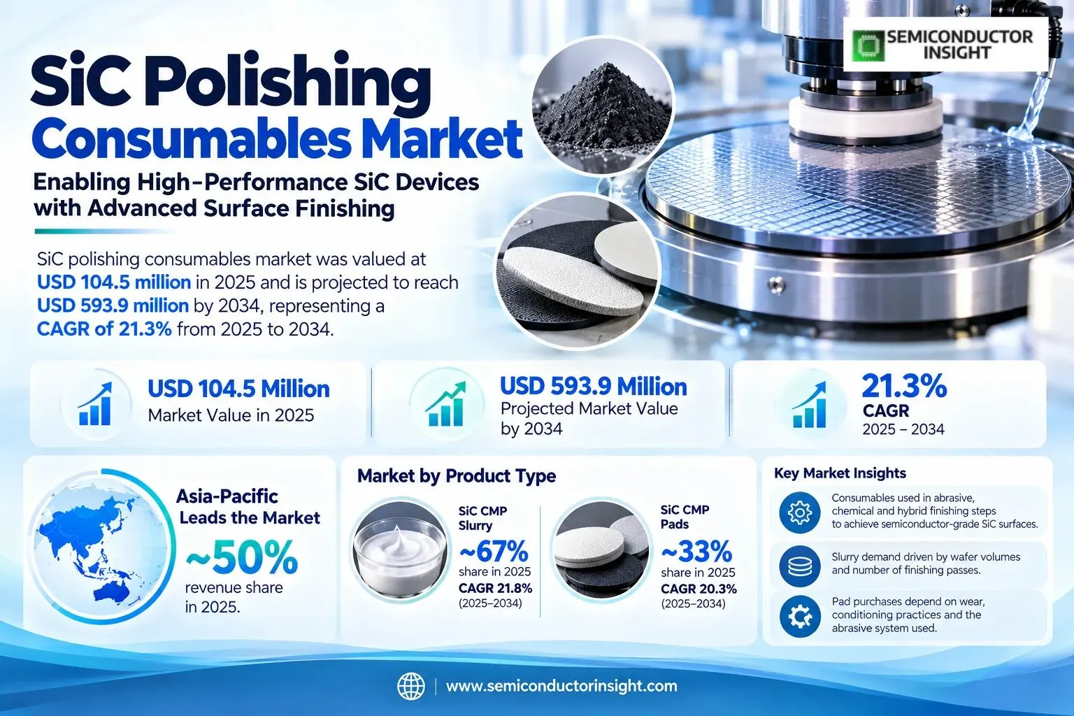
- Market trajectory: Global sales of wafer polishing consumables used on silicon carbide substrates reached USD 104.5 million in 2025 and are projected to attain USD 593.9 million by 2034, equivalent to 21.3% compound growth across the nine-year interval.
- 2026 transition: The 2026 market estimate is USD 126.7 million; qualification of 200 mm wafer finishing processes supports new slurry formulations, precision pads and tighter controls over scratches, roughness and thickness variation.
- Product mix: SiC CMP slurry accounts for an estimated ~67% of 2025 sales, while polishing and lapping pads contribute ~33%; the two products are purchased together but differ in replacement cadence and formulation requirements.
- Wafer diameter: Six-inch SiC wafers represent the largest application at ~55% of consumables demand, ahead of eight-inch wafers at ~25% and four-inch substrates at ~20%, with the 200 mm transition lifting the newer diameter class.
- Regional position: Asia-Pacific leads with ~50% of revenue, followed by North America at ~26%, Europe at ~17%, South America at ~4% and the Middle East and Africa at ~3%, reflecting differences in substrate fabrication and supply-chain location.
Global SiC Polishing Consumables Market Overview
SiC polishing consumables market was valued at USD 104.5 million in 2025 and is projected to reach USD 593.9 million by 2034, representing a CAGR of 21.3% from 2025 to 2034. Consumables are used in the abrasive, chemical and hybrid finishing steps that turn hard, brittle silicon carbide crystals into semiconductor-grade surfaces; Asia-Pacific held the largest estimated revenue share in 2025 at ~50%.
Silicon carbide is unusually demanding to finish because the substrate combines high hardness with a chemically resistant surface. Wafer makers therefore use several operations rather than a single polish: rough flattening, controlled material removal, damage reduction and final chemical-mechanical polishing. Slurry chemistry and pad construction influence how much material is removed per hour, whether deep scratches survive, and whether the wafer is sufficiently flat for subsequent epitaxy. Revenue arises from repeat purchases of those consumables, not from the value of the wafer itself.
The economics of polishing depend on yield as much as throughput. An aggressive abrasive can remove subsurface damage quickly but may create defects that later reduce device yield, whereas a gentler finishing step can consume more machine time. Saint-Gobain describes abrasive-free permanganate chemistry for its ClasSiC 2000 family, while Entegris offers dedicated formulations for both batch and single-wafer processing. Such product distinctions explain why fabs qualify several chemical and pad combinations rather than selecting solely on slurry price per litre.
The transition from 150 mm to 200 mm substrates changes the operating envelope of a polishing line. Larger disks increase the surface area processed per wafer and place more emphasis on uniform pressure, slurry delivery and edge performance. A process that achieves acceptable roughness on a 6-inch substrate may require fresh pad conditioning and chemistry tuning at 8 inches. Infineon announced initial products from its 200 mm SiC production in Villach during February 2025, showing that larger-diameter material is entering commercial device workflows rather than remaining only a laboratory demonstration.
Demand is also linked to the number of polishing passes and to how frequently a fab changes pads or replenishes slurry. Higher wafer starts raise liquid consumption, but a process improvement that increases removal rate can reduce chemistry per unit of output. Suppliers therefore sell on total cost of ownership, measured through usable wafers, rework rates, pad lifetime, slurry stability and contamination control. This creates a market where technical support and qualification data can be as important as factory scale.
The commercial boundary includes silicon carbide CMP slurry, associated polishing pads and specified lapping-pad consumables used on 4-inch, 6-inch and 8-inch SiC semiconductor wafers. It excludes grinding and polishing machines, complete bare substrates, finished power MOSFETs, and CMP formulations sold only for conventional silicon or metal interconnects. Within this boundary, the model separates a mature six-inch installed base from the faster-growing eight-inch process migration, while recognizing that specialty four-inch lines remain operational.
Segment Analysis: By Type
By product type, the market contains SiC CMP Slurry and SiC CMP Pads. Slurry holds an estimated ~67% of 2025 value and grows at ~21.8% annually in the private allocation, whereas pads hold ~33% and expand at ~20.3%. Slurry demand responds to the quantity of wafers and number of finishing passes; pad purchases depend more strongly on wear, conditioning practices and the abrasive system used.
| Type | Function | Market position |
|---|---|---|
| SiC CMP Slurry | Chemical-mechanical polishing liquids combine reactive ingredients with abrasive or abrasive-free mechanisms to remove material from hard SiC surfaces. Process engineers choose chemistry by required removal rate, target roughness, particle contamination, shelf stability and compatibility with a specific pad. Entegris markets separate batch and single-wafer formulations, while Saint-Gobain offers a permanganate-based option that uses chemical modification rather than suspended abrasive particles. | Largest type, ~67% of 2025 revenue; modeled growth ~21.8%. Slurry is replenished continuously and can require multiple recipes across rough, intermediate and final steps. The category benefits from 8-inch substrate adoption, where uniform distribution and defect suppression carry greater economic value. Premium formulations compete on process yield and removal consistency rather than only on price per kilogram, and customers usually validate them over many wafer lots. |
| SiC CMP Pads | Polishing pads transmit pressure, manage contact mechanics and carry slurry or embedded abrasive against the wafer surface. Pad selection varies between rough lapping, pre-CMP damage removal and final planarization, with conditioning and backing construction affecting contact uniformity. Fujibo NEXTILE T-series embeds diamond grains into pads for hard materials, whereas other pad families rely on liquid abrasives and controlled polymer surface textures. | Estimated ~33% share with ~20.3% modeled growth. Pads are replaced after wear, glazing, edge nonuniformity or a change in process recipe, so purchases are tied to equipment utilization and operating discipline. Suppliers gain position by documenting scratch reduction and predictable lifetime. A pad that lasts longer may lower unit consumption yet still command a higher selling price when it improves good-wafer output. |
Process selection: removal rate, finish and wear
A polishing consumable is not interchangeable across all steps. Rough lapping emphasizes controlled stock removal, intermediate polishing reduces subsurface damage, and final CMP aims for a surface suitable for epitaxial deposition. Entegris differentiates SiC slurry products by batch or single-wafer operation, and Saint-Gobain distinguishes abrasive-free chemistry from nano-alumina-containing formulations. The process sequence, rather than a single universal recipe, determines how the ~67% slurry and ~33% pad shares translate into purchasing contracts.
The transition to 200 mm processing introduces a second design challenge: maintaining uniform polishing across a larger disk while avoiding edge exclusion losses. Slurry distribution, pad compressibility and platen conditions interact with wafer bow and thickness variation. Commercial evaluations therefore combine removal-rate tests with scratch inspection, total thickness variation and post-polish cleanliness. A consumable that shortens one process step but increases downstream rework may lose a supply award despite a lower nominal purchase price.
Segment Analysis: By Application
The application axis follows the diameter of the SiC wafer: 4 Inch SiC Wafer, 6 Inch SiC Wafer and 8 Inch SiC Wafer. Six-inch processing leads with an estimated ~55% share in 2025, eight-inch contributes ~25% and four-inch accounts for ~20%. Modeled annual growth is strongest in 8-inch polishing at ~23.5%, followed by 6-inch at ~20.9% and 4-inch at ~19.3%.
| Application | Demand characteristics |
|---|---|
| 4 Inch SiC Wafer | Estimated ~20% of 2025 sales; modeled ~19.3% CAGR. Four-inch wafers remain relevant in legacy power-device lines, research environments and specialized applications where qualification of existing equipment outweighs the economic benefits of a diameter conversion. Their smaller surface area allows mature pad geometries and established polishing recipes, but lower volumes limit supplier incentives to create new dedicated formulations. Replacement demand follows continuing wafer starts rather than new factory announcements. |
| 6 Inch SiC Wafer | Largest application, ~55% of value; modeled ~20.9% CAGR. The 150 mm format supports a substantial installed base of substrate production and device fabrication, generating recurring demand for CMP slurry, pre-polish pads and final finishing media. Buyers optimize removal rate, subsurface damage and total thickness variation across established tools. Suppliers with validated batch and single-wafer chemistry can defend accounts through repeatable performance and technical service. |
| 8 Inch SiC Wafer | Estimated ~25% share; fastest modeled growth ~23.5%. The 200 mm format offers more die area per wafer but places stricter demands on polishing uniformity, edge control and low-defect finishing. Device manufacturers are expanding qualification of 200 mm materials, including Infineon production and Wolfspeed substrate offerings. Consumables suppliers must adapt pads, chemistry and conditioning routines, creating premium sales opportunities before larger-diameter processing becomes fully standardized. |
The 4-inch, 6-inch and 8-inch groups describe the size of the wafer being finished, not three different chemical products. A single supplier may sell several slurry grades across all three diameters, but the recipe and pad qualification can differ substantially. The 6-inch installed base creates dependable replenishment demand today, while 8-inch process transfer offers more scope for newly designed chemistry and application engineering. Four-inch polishing continues where specialized device requirements make conversion uneconomic.
Larger wafer formats alter commercial negotiations because a polishing defect can affect a greater number of potential chips on one substrate. Purchasing teams therefore compare consumables by defect density, surface roughness, usable area and repeatability across production lots. An increase in price per litre can be accepted if a formulation reduces scrap or shortens a finishing step. Conversely, a pad with low upfront cost may be rejected when frequent conditioning reduces throughput or changes the wafer profile.
Regional Analysis
Asia-Pacific is the leading SiC polishing consumables region at an estimated ~50% of 2025 sales, reflecting the concentration of wafer processing and material supply chains in East Asia. North America contributes ~26%, Europe ~17%, South America ~4%, and the Middle East and Africa ~3%. The regional pattern is influenced by where substrates are actually finished rather than by the location of final electric-vehicle sales.
Where are SiC polishing consumables purchased and qualified?
Polishing consumables follow wafer finishing operations, which can be geographically separate from device assembly or vehicle production. Asia-Pacific has broad materials and specialty-chemical capability, while the United States combines domestic substrate programs with slurry suppliers and technical support. European demand is tied to automotive-grade power semiconductor supply chains and process qualification at device makers. Smaller markets participate through specialty polishing, laboratory work and import distribution, rather than through large clusters of SiC crystal growth.
The private regional allocation assigns ~50% to Asia-Pacific, ~26% to North America, ~17% to Europe, ~4% to South America and ~3% to the Middle East and Africa. These are estimates of consumables revenue, not published regional totals for wafer substrates. Growth differs by regional investment timing: Asia-Pacific has modeled ~22.6% annual expansion, North America ~19.2%, Europe ~20.2%, South America ~21.6% and the Middle East and Africa ~20.3%.
| Region | Position | Growth outlook | Demand profile | What decides supplier selection |
|---|---|---|---|---|
| Asia-Pacific | Largest (~50%) | Fastest (~22.6% CAGR) | Wafer production and local pad chemistry | High-volume qualification, defect performance and reliable local technical support |
| North America | Second (~26%) | Established (~19.2% CAGR) | Substrate finishing and advanced materials | Process documentation, purity controls and continuity of supply |
| Europe | Third (~17%) | Technology-led (~20.2% CAGR) | Automotive-grade SiC process transfers | Yield consistency, traceability and supplier co-development |
| South America | Smaller (~4%) | Developing (~21.6% CAGR) | Specialty polishing and imported media | Distributor access, price stability and qualified process support |
| Middle East & Africa | Emerging (~3%) | Selective (~20.3% CAGR) | Pilot production and research activities | Training, equipment compatibility and low-volume availability |
Key SiC Polishing Consumables Manufacturers and Competitive Landscape
Competition in SiC polishing consumables combines specialty chemical formulation, engineered pad surfaces and application engineering. Entegris, Saint-Gobain, Fujimi and Fujibo have documented products relevant to hard-substrate finishing, while DuPont and other CMP suppliers provide adjacent semiconductor pad expertise. Customer qualification is demanding because changing either slurry or pad can alter scratches, removal rate and downstream yield, which gives validated products considerable staying power.
Entegris competes through dedicated slurry chemistry and its ability to support high-purity manufacturing processes. Its catalog distinguishes SiC products for batch and single-wafer polishing, giving customers a route to tune removal rate and final surface condition. A chemical supplier must also control particle distribution, contamination and shelf stability from one lot to the next, so consistent manufacturing and responsive application engineers can be more important than an aggressive introductory price.
Saint-Gobain differentiates its surface-conditioning portfolio through chemistry choice. The ClasSiC 2000 abrasive-free series relies on chemical surface modification, while the ClasSiC 2100 family uses nano-alumina abrasive particles. These alternatives address different polishing objectives and equipment configurations. Buyers may qualify both types at different process stages, allowing a supplier with multiple chemistries to participate in more of the wafer finishing sequence without claiming the same revenue twice.
Pad-focused suppliers compete through contact mechanics, abrasive integration and usable lifetime. Fujibo markets NEXTILE products for difficult-to-machine materials including SiC, and 3M documents Trizact pads and composite slurry products for hard-substrate lapping. A diamond-embedded pad can reduce reliance on free abrasive in a rough step, whereas a softer final-polish pad is chosen for surface integrity. The best-performing system is determined by the entire recipe, not by one consumable in isolation.
The wider supplier field includes Fujimi, Engis and regional specialists in China. Some companies are known for general semiconductor CMP rather than independently documented SiC-specific revenue, and their presence should be interpreted as technological capability or potential competition rather than a measured market ranking. The acquisition of CMC Materials by Entegris means legacy CMC names must not be double-counted as separate present-day suppliers. Customers continue to assess chemical compatibility and support alongside cost.
Tier structure
| Tier | Companies | Basis of competition |
|---|---|---|
| Dedicated SiC chemistry | Entegris; Saint-Gobain; Fujimi Corporation | Documented slurry products for SiC polishing, including abrasive-free or specialized chemical formulations and process-specific performance targets. These suppliers can influence removal rate, surface integrity and defect control, and their technical support is relevant when customers migrate from 150 mm to 200 mm wafers. Long qualification cycles favor firms able to reproduce results over many manufacturing lots. |
| Engineered pads and lapping media | Fujibo Group; 3M; Engis; DuPont | Suppliers with engineered pad, abrasive or broader CMP capability that can address stages of SiC wafer preparation. Competitive differentiation rests on contact uniformity, embedded abrasive design, wear rate and compatibility with liquid chemistry. Not every general CMP pad is proven for SiC, so qualification evidence is more useful than a generic product-category listing. |
| Regional and specialist participants | Shanghai Xinanna Electronic Technology; Beijing Hangtian Saide; Beijing Grish Hitech; Tianjin Helen; CHUANYAN; Ferro / UWiZ Technology | Companies appearing in the SiC polishing supply landscape, particularly in regional chemical and surface-finishing markets. Product breadth and commercial scale differ, and publicly accessible information does not support assigning precise supplier shares. Local relationships, delivery speed and adaptation to domestic polishing equipment may provide an advantage where customers are building their first qualified wafer finishing lines. |
Key companies profiled
- Entegris (including CMC Materials)
- Saint-Gobain
- Fujimi Corporation
- Fujibo Group
- DuPont
- 3M
- Engis
- Shanghai Xinanna Electronic Technology
- Beijing Hangtian Saide
- Beijing Grish Hitech
- Tianjin Helen
- CHUANYAN
- Ferro / UWiZ Technology
SiC Polishing Consumables Production Capacity Analysis
Production capacity is distributed between specialty chemical plants, abrasive-material operations and engineered pad manufacturing rather than concentrated in a single wafer-fab process. Suppliers must scale high-purity formulations while keeping particle-size distribution, chemical stability and packaging consistent. Customers judge available capacity by qualified lots and assured delivery schedules, not merely by the nominal output of a mixing vessel or coating line.
Slurry manufacturing requires controlled blending, filtration, metrology and contamination prevention. High-removal chemistries may use abrasive particles, while abrasive-free formulations depend on precise reactive composition and contact with the pad. Batch-to-batch reproducibility is essential because a small change in polishing performance can alter wafer flatness or surface defects. For 200 mm production, customers also need dependable logistics and lot traceability as chemical consumption increases with wafer throughput.
Pad manufacturing follows a different industrial path involving polymer structure, abrasive integration, surface finishing and dimensional conversion. Fujibo describes NEXTILE T-series diamond grain sizes near 4 and 9 micrometres, illustrating the precision required to maintain consistent cutting action. Pads may be produced in standard sheets and converted into shapes suited to individual tools, but customers still require validation of backing adhesion, thickness, conditioning behavior and edge wear.
Capacity expansion is not automatically proportional to market growth because more effective formulations can reduce the amount of chemistry needed per wafer. A slurry that removes material faster can shorten processing time, while a longer-lived pad can lower replacement frequency. At the same time, larger 8-inch wafers and rising production starts increase total surface area processed. Suppliers therefore plan production around qualified process recipes and replenishment rates rather than only announced substrate factory capacity.
SiC Polishing Consumables Market Dynamics
The principal demand drivers are wider adoption of SiC power devices, the migration to 200 mm substrates, increasingly stringent wafer-surface specifications and the replenishment of consumables in existing lines. Costs and technical qualification limit the pace of adoption: polishing chemistry is specialized, abrasive and pad performance can interact unpredictably, and manufacturers avoid recipe changes that threaten yield. The impact analysis attributes positive and negative contributions to the 2025–2034 growth trajectory.
MARKET DRIVERS
Drivers Impact Analysis*
| Market Drivers | Impact Rank | CAGR Contribution (%) | 2026–2028 | 2029–2031 | 2032–2034 |
|---|---|---|---|---|---|
| Growth in SiC power-device wafer starts | High | +9.10% | High | High | Medium |
| Migration to 200 mm substrate polishing | High | +6.30% | Medium | High | High |
| Higher surface-quality and yield requirements | Medium-High | +4.50% | High | High | High |
| More finishing steps and specialty chemistries | Medium | +3.30% | Medium | High | High |
| Local sourcing and process qualification | Low-Medium | +1.80% | Medium | Medium | High |
| Others (research wafers, pilot lines, pad innovation) | Low | +1.20% | Low | Medium | Medium |
Device wafer starts sustain recurring consumables sales
Every finished SiC substrate passes through multiple surface preparation operations before it can support high-quality device layers. Growing adoption of power devices in traction inverters, chargers and industrial conversion equipment therefore increases the total area that must be polished. Unlike capital equipment, slurry is replenished and pads wear out during production, creating a recurring revenue stream tied to wafer starts. This demand persists after a fabrication plant completes its initial equipment purchase.
Two-hundred-millimetre processing raises specification value
The 200 mm transition increases the number of potential die per wafer but also makes edge effects and within-wafer uniformity more consequential. Suppliers must adapt chemical delivery, pad design and conditioning to larger substrates. Infineon has demonstrated commercial 200 mm device production, and Wolfspeed offers premium 200 mm starting material. These downstream and upstream milestones support qualification spending on polishing consumables without constituting direct sales figures for those products.
Lower defectivity becomes a purchasing differentiator
Subsurface damage, scratches and residual particles can undermine epitaxy and ultimately reduce device yield. Saint-Gobain describes an abrasive-free SiC CMP route intended to limit particle-induced defects, while Entegris differentiates formulations by process configuration and removal requirements. Buyers increasingly compare consumables using good-wafer output, not just immediate polishing speed. That favors chemistry suppliers able to document stable surface integrity and pad producers able to maintain consistent contact conditions.
Process specialization expands the value of each qualification
A high-volume SiC wafer may encounter rough lapping, intermediate polishing and final CMP, each requiring a different balance between stock removal and surface finish. Specialized slurry grades and pads can be qualified separately for those operations, increasing the value of technical support and inventory management. Customers still seek to reduce unnecessary passes, so growth comes from useful process specialization rather than an assumption that every wafer must consume more material indefinitely.
MARKET RESTRAINTS
Restraints Impact Analysis*
| Market Restraints | Impact Rank | CAGR Contribution (%) | 2026–2028 | 2029–2031 | 2032–2034 |
|---|---|---|---|---|---|
| High-purity formulation and abrasive costs | High | -1.80% | High | High | Medium |
| Long qualification cycles and recipe lock-in | Medium-High | -1.30% | High | Medium | Medium |
| Process efficiency reducing use per wafer | Medium | -1.10% | Medium | High | High |
| Others (chemical logistics, pad wear variability) | Low | -0.70% | Medium | Medium | Low |
Specialty inputs limit the scope for rapid price reductions
Semiconductor-grade slurries require tight particle and impurity controls, and engineered pads use materials whose consistency affects contact mechanics. Producing a stable formulation at scale involves filtration, testing and specialized packaging, which adds cost beyond commodity abrasives. A customer can justify the premium when yield improves, but early-stage fabs may delay adoption of the newest consumable until throughput and defect performance are demonstrated over enough production lots.
Process requalification makes supplier switching slow
A polishing recipe is an integrated combination of chemistry, pad, pressure, conditioning and cleaning. Replacing one component can change removal rate or defect distribution even when the substitute appears similar in a supplier specification. Semiconductor manufacturers therefore run extended tests before approving a change, especially for automotive-grade material. This protects incumbent suppliers but can delay commercial acceptance of innovative products and lengthen the sales cycle for new entrants.
Higher efficiency can offset physical consumption growth
Some new formulations promise greater removal rate, lower abrasive residue or longer pad life, and these improvements can reduce the consumable quantity needed for a given wafer output. Saint-Gobain identifies dilutability and potential recycling for its abrasive-free product family, while embedded-abrasive pads can change slurry requirements in lapping. Consequently, the revenue opportunity depends on a balance of wafer-start growth, product mix and consumption efficiency rather than on surface area alone.
MARKET OPPORTUNITIES
Qualification packages for 200 mm wafer lines
The shift to 8-inch SiC substrates creates an opportunity to sell chemistry and pad systems as a qualified package instead of as unrelated supplies. Customers need data on removal rate, total thickness variation, edge performance and post-CMP cleanliness across larger wafers. Suppliers that provide application support and repeatable testing can gain an early position in new lines, even where initial volumes are lower than the installed 6-inch base.
Abrasive-free final polishing and lower cleaning burden
Final polishing increasingly values defect suppression and surface integrity, especially when subsequent epitaxy is sensitive to residual damage. Abrasive-free permanganate chemistry offers one technical route, while controlled nano-abrasive formulations provide another. The opportunity lies in matching these approaches to specific tool and pad combinations and demonstrating lower overall cost per qualified wafer, rather than asserting that one chemistry is universally superior.
Localized technical service for emerging substrate producers
New SiC wafer manufacturers in Asia and other regions may lack a long history of pad conditioning and slurry control. Consumables suppliers can differentiate themselves by offering process development, metrology support, small-lot trials and rapid troubleshooting. Once a recipe meets yield targets, recurring orders can follow as wafer starts rise. This service-led route is particularly useful where domestic suppliers compete with established multinational chemical companies.
SiC Polishing Consumables Supply Chain Analysis
The value chain begins with high-purity chemical ingredients, abrasive particles and pad polymers, continues through controlled formulation and pad fabrication, and ends with qualification at substrate finishing facilities. A supplier’s commercial position depends on how reliably it links these stages. A low-cost ingredient is of limited value if variability increases defects or if the final consumable cannot be delivered in the packaging and purity grade required by a semiconductor customer.
Raw materials. The upstream supply base includes specialty oxidizers, abrasive particles, engineered polymers and high-purity process water. Contamination control matters because trace impurities or large particles can cause scratches or defects on SiC surfaces. Producers need stable feedstock specifications and reliable analytical testing, especially when serving customers with automotive or high-voltage device programs. A material supplier that cannot document purity and particle behavior may be excluded before any polishing trial begins.
Formulation and pad production. Slurry manufacturers control mixing, dispersion, filtration and packaging, whereas pad producers engineer surface texture, hardness, thickness and abrasive content. These capabilities are complementary but operationally different. Entegris and Saint-Gobain document chemistry approaches for SiC, while Fujibo and 3M provide pad and lapping-media examples. Product performance emerges from the interaction of both consumables with a particular tool, not from an isolated catalog specification.
Qualification and distribution. Before a customer commits to production purchases, the consumables combination is tested for material removal, surface roughness, thickness variation, particle contamination and repeatability. Distribution then requires storage practices that protect chemistry quality and preserve lot traceability. Regional technical support can shorten troubleshooting when a process drifts. The qualification stage creates switching costs, which is why long-term customer relationships are common even in a market with several competing material suppliers.
End-use processing. Substrate finishers buy consumables to prepare wafers for epitaxy and device manufacturing, while research facilities purchase smaller quantities for process development. Six-inch lines account for the largest modeled application share at ~55%, but eight-inch qualification is growing faster as 200 mm projects mature. Finished MOSFET or vehicle sales are downstream demand signals and must not be counted as polishing-consumables revenue; the relevant purchase is the slurry or pad used in wafer preparation.
Recent Developments in SiC Polishing Consumables and Wafer Processing
- 15 October 2026 WAFER SUPPLY
Infineon and Wolfspeed announced an extension of their silicon carbide wafer supply relationship to include 200 mm substrates. This is a substrate procurement agreement rather than a polishing chemistry contract, but it confirms customer attention to larger-diameter material. For consumables suppliers, the significance is the need to qualify pads and slurries that maintain consistent finish and defect performance on production-scale 8-inch wafers. Source - 27 September 2026 SUBSTRATE QUALITY
Wolfspeed introduced a premium n-type 200 mm silicon carbide substrate offering, citing improvements in defect density and wafer-shape stability. The announcement relates to wafer material, not consumables revenue. It nevertheless sets a useful commercial context: upstream polishing must preserve the surface quality achieved during crystal and substrate processing, so suppliers of finishing materials compete on repeatable defect suppression and within-wafer uniformity. Source - 13 February 2025 DEVICE MANUFACTURING
Infineon announced first power semiconductor products manufactured using 200 mm SiC wafers at its Villach site. The milestone shows that the larger format is entering commercial device manufacturing, although the company did not disclose polishing slurry purchases. Consumables producers can use such process transfers to develop 200 mm pad dimensions, chemical delivery routines and qualification packages designed for tighter flatness and defect requirements. Source - 16 October 2025 CMP PAD SUPPLY
DuPont reported a long-term CMP pad supply agreement involving Qnity and SK hynix, illustrating the strategic importance of qualified polishing consumables in the wider semiconductor industry. The agreement concerns a broader CMP customer relationship and is not evidence of SiC-specific pad sales. Its relevance lies in showing why process stability, multi-year supply and customer qualification are central commercial capabilities for pad manufacturers. Source - 13 February 2019 SLURRY PRODUCT
Fujimi described COMPOL 202 SC and DSC 0902 slurries for high-volume SiC wafer polishing in the United States. Although older than the other milestones, this product announcement establishes a documented technical foundation for SiC-specific chemical consumables. The continuing commercial significance is the distinction between specialized epi-ready substrate finishing and general-purpose CMP chemistry designed for unrelated semiconductor layers. Source
REPORT SCOPE & SEGMENTATION
| Attribute | Details |
|---|---|
| Report Title | Global SiC Polishing Consumables Market Size, Share and Industry Analysis |
| Market Size 2025 | USD 104.5 million |
| Market Size 2026 | USD 126.7 million |
| Market Size 2034 | USD 593.9 million |
| Growth Rate | CAGR of 21.3% from 2025–2034 |
| Unit | Value in USD million; pad and slurry consumables revenue |
| Historical Reference | 2023–2024 |
| Base / Estimate / Forecast | 2025 base year; 2026 estimate; 2034 forecast |
| By Type | SiC CMP Pads · SiC CMP Slurry |
| By Application | 4 Inch SiC Wafer · 6 Inch SiC Wafer · 8 Inch SiC Wafer |
| By Region | Each region evaluated by consumables type, wafer diameter and country-level processing role North AmericaUnited States, Canada, Mexico EuropeGermany, France, Austria, Italy, Rest of Europe Asia-PacificChina, Japan, South Korea, Taiwan, India, Rest of Asia-Pacific South AmericaBrazil, Argentina, Chile, Colombia, Rest of South America Middle East & AfricaIsrael, UAE, Saudi Arabia, South Africa, Rest of Middle East & Africa |
| Key Companies Profiled | Entegris (CMC Materials), Saint-Gobain, Fujimi Corporation, Fujibo Group, DuPont, 3M, Engis, Shanghai Xinanna Electronic Technology, Beijing Hangtian Saide, Beijing Grish Hitech, Tianjin Helen, CHUANYAN, Ferro / UWiZ Technology |
| Customization Scope | Custom country, wafer-diameter and pad/slurry breakdowns, process application splits and selected substrate-finishing demand analysis can be added to the standard coverage. |
Frequently Asked Questions
What is the size and growth rate of the SiC polishing consumables market?
The global market reached USD 104.5 million in 2025 and is projected to expand to USD 593.9 million by 2034, corresponding to a 21.3% CAGR across the 2025–2034 period. The 2026 estimate is USD 126.7 million. Growth is tied to higher SiC wafer starts, more stringent surface-quality requirements and the gradual move from 150 mm toward 200 mm substrate processing.
What products are included in SiC polishing consumables?
The market includes SiC CMP slurry and polishing or specified lapping-pad consumables used to prepare semiconductor-grade silicon carbide wafers. Slurries may be abrasive or abrasive-free, and pads can be engineered for rough, intermediate or final finishing. The boundary excludes wafer manufacturing machines, finished SiC substrates, power devices and CMP products sold only for conventional silicon or metal interconnect processing.
Which product type holds the largest market share?
SiC CMP slurry is the largest product category, with an estimated ~67% of 2025 revenue, compared with ~33% for CMP and related polishing pads. Slurry is replenished as wafers are processed and can involve several recipes for different finishing steps. Pads have a different purchasing rhythm, determined by wear, conditioning and changes in the qualified process combination.
Which wafer diameter drives the greatest consumables demand?
Six-inch SiC wafers represent the largest application, accounting for an estimated ~55% of polishing consumables revenue in 2025. Eight-inch processing contributes ~25% and is growing more quickly as 200 mm projects enter commercial production, while four-inch wafers retain ~20% in mature and specialized operations. Larger diameters create fresh requirements for uniformity, edge performance and defect suppression.
Why are 200 mm wafers important for polishing suppliers?
A 200 mm substrate provides more surface area and potential chips than a 150 mm wafer, but it also exposes nonuniform pressure, pad wear and edge effects across a larger disk. Process engineers may need new pad constructions, slurry delivery settings and cleaning routines. The transition therefore creates opportunities for qualified consumables even before every substrate manufacturer reaches full-scale eight-inch output.
Which region leads global demand?
Asia-Pacific is the largest regional market with an estimated ~50% of 2025 consumables sales, reflecting local wafer processing and the presence of Japanese and Chinese materials suppliers. North America follows at ~26%, Europe at ~17%, South America at ~4%, and the Middle East and Africa at ~3%. These shares refer to consumables purchases rather than the location of downstream electric-vehicle sales.
What are the principal growth drivers?
Increasing SiC power-device wafer starts, larger-diameter substrate migration and tighter surface-quality specifications are the main drivers. More wafer area must be flattened and polished, and process teams are willing to qualify specialized chemistry when it improves usable wafer yield. Recurring slurry replenishment and pad replacement make consumables demand different from one-time capital equipment investment.
What limits the adoption of new CMP slurries and pads?
High-purity chemical production, specialty abrasive costs and lengthy process qualification can slow adoption. A change in slurry or pad may alter removal rate, scratch formation or residual contamination, requiring many tests before automotive-grade customers approve it. Better removal efficiency and longer pad life can also reduce the amount of consumable used per wafer, offsetting part of volume growth.
Which manufacturers participate in this market?
The supplier landscape includes Entegris, Saint-Gobain, Fujimi, Fujibo, DuPont, 3M, Engis and several regional Chinese specialists. Their roles differ: some sell dedicated SiC slurries, others supply engineered pads or broader semiconductor CMP materials. Entegris acquired CMC Materials, so those names should not be counted as separate independent present-day companies when interpreting the competitive structure.
How is the market segmented and what period is covered?
The market uses 2025 as its base year, 2026 as its estimate year and 2034 as its forecast endpoint, with historical context from 2023 and 2024. Segmentation is by SiC CMP pads versus slurry and by 4-inch, 6-inch and 8-inch wafer application. Geographic coverage includes five major regions and country-level discussion of wafer processing and supplier activity.
Research Sources & Evidence Base
Get Sample Report PDF for Exclusive Insights
Report Sample Includes
- Table of Contents
- List of Tables & Figures
- Charts, Research Methodology, and more...
 Download Sample Report PDF