
Key Statistics
Key Takeaways
- 300MM Polishing Machine is the leading product type and accounts for the clear majority of demand because advanced logic, memory and high-volume foundry capacity is concentrated on 300mm wafers.
- Semiconductor Plants dominate application demand because CMP is embedded in front-end interconnect, isolation, gate-stack and advanced-packaging process flows.
- Asia leads the market with more than two-thirds of global demand in the report scope, driven by semiconductor manufacturing clusters in Taiwan, South Korea, China and Japan.
- Advanced packaging is creating a new CMP growth layer. Applied Materials introduced Opta Quad CMP in 2026 for hybrid bonding and stacked AI packages where surface planarity directly affects yield.
- Panel-level packaging expands the addressable equipment base. EBARA is developing panel-level CMP for large organic interposers through the JOINT3 consortium.
- Process control is moving closer to real time. Endpoint detection, in-line metrology, profile control and post-CMP cleaning are becoming core machine differentiators as defect tolerance narrows.
Chemical Mechanical Polishing Machine (CMP) Market Overview
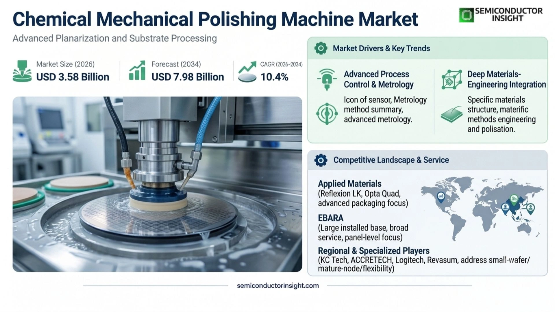
Chemical Mechanical Polishing Machine Market was valued at USD 3,240.0 million in 2025, is estimated at USD 3,581.5 million in 2026, and is projected to reach USD 7,983.1 million by 2034, representing a CAGR of 10.5% during 2026–2034. Asia is the largest market in 2025, while the commercial growth mechanism is increasingly shaped by AI-driven 300mm fab investment, advanced-node logic, HBM and DRAM, higher-layer 3D NAND, hybrid bonding, panel-level packaging, and tighter planarization control.
Chemical mechanical polishing machines planarize semiconductor wafers by combining controlled mechanical abrasion with chemistry. The equipment presses the wafer against a polishing pad while slurry removes dielectric, copper, tungsten, barrier and other films. CMP is essential because advanced chips are built through many repeated deposition and patterning steps, and each new layer requires a sufficiently flat surface for later lithography and interconnect formation.
Demand is rising with the number of CMP steps per wafer as device architectures become more three-dimensional. Leading-edge logic uses complex metal stacks and gate-all-around structures, HBM and advanced packaging require very flat bonding surfaces, and 3D NAND adds more process complexity as layer counts rise. These trends increase both installed tool demand and the value of endpoint, cleaning and defect-control features.
Equipment economics depend on throughput, within-wafer uniformity, consumable stability and uptime. A modern tool combines polishing heads, multiple platens, slurry delivery, pad conditioning, wafer cleaning, metrology and software control. Applied Materials and EBARA lead the high-end market through deep process integration, while regional competitors address mature-node, research and domestic-fab requirements.
Segment Analysis: By Type
By type, the market is segmented into 300MM Polishing Machine, 200MM Polishing Machine, and Others. 300mm systems lead because the largest investments in advanced logic, DRAM, HBM and high-volume foundry production use 300mm wafers.
| Type | Technical role | Market position |
|---|---|---|
| 300MM Polishing Machine | High-throughput platforms designed for modern 300mm logic, memory and foundry fabs. They integrate multiple platens, sophisticated endpoint control, cleaning and automated wafer handling. | The leading type. SEMI expects record 300mm equipment investment in 2026, supporting continued demand for advanced CMP capacity. |
| 200MM Polishing Machine | Systems serving mature-node analog, power, MEMS, sensors and specialty semiconductor production where 200mm fabs remain economically attractive. | A stable installed-base segment. SEMI’s 2026 200mm outlook shows continued investment in mature-node capacity, supporting replacement and expansion demand. |
| Others | Includes smaller-wafer research systems, panel-level packaging CMP and specialized polishing platforms for compound semiconductors or advanced substrates. | A smaller but strategically important category as packaging and specialty materials create new planarization requirements beyond conventional 200/300mm wafers. |
Why does 300mm CMP capture most new equipment value?
Advanced logic, DRAM and NAND manufacturers build their newest high-volume capacity on 300mm wafers because larger wafer area lowers cost per die when yields and utilization are high. These fabs also use more sophisticated interconnect and planarization steps. SEMI’s 2026 300mm outlook points to record front-end equipment spending, while Applied’s Reflexion LK and Opta Quad platforms show how new CMP value is concentrated in high-throughput 300mm and advanced-packaging applications.
Segment Analysis: By Application
By application, the market is segmented into Semiconductor Plants and Research Institutes. Semiconductor Plants dominate because CMP is a production-critical process repeated across logic, memory and advanced-packaging flows.
| Application | Demand characteristics | Market position |
|---|---|---|
| Semiconductor Plants | High-volume fabs use CMP for oxide, copper, tungsten, shallow-trench isolation, gate-stack and packaging planarization. Tool uptime and defectivity directly affect wafer output. | The dominant application. New fab capacity, node migrations and additional process steps create both greenfield tool demand and upgrades at installed fabs. |
| Research Institutes | Universities, national laboratories and pilot lines use smaller or configurable polishing systems to develop new films, packaging structures and compound-semiconductor processes. | A smaller application with high technical value. Research systems emphasize flexibility, recipe development and material experimentation rather than maximum wafer throughput. |
Why is advanced packaging becoming a major CMP application?
Hybrid bonding and stacked AI packages require extremely flat copper and dielectric surfaces before two wafers or dies can be joined. Thick films and large topography in packaging also create different process conditions from front-end CMP. Applied Materials launched Opta Quad specifically for advanced packaging, while EBARA is developing panel-level polishing for large organic interposers, showing that planarization is expanding into the back end as packaging becomes a performance technology.
Regional Analysis
Asia is the largest reported CMP equipment market, with the report scope assigning it more than 68% share in 2025. The five-region view is led by Asia Pacific through Taiwan, South Korea, China and Japan, followed by North America and Europe as regional fab investment increases.
Why is CMP demand concentrated in Asia while investment is broadening globally?
Asia Pacific contains the largest installed base of leading foundry and memory fabs, which creates recurring demand for CMP tools, spare parts and service. North America and Europe are adding strategic semiconductor capacity through regionalization programs, while India and Southeast Asia are building new electronics and semiconductor ecosystems. The result is continued Asian leadership with faster diversification of incremental equipment demand.
| Region | Position | Growth outlook | Demand profile | What decides supplier selection |
|---|---|---|---|---|
| Asia Pacific | Largest reported market | Very strong | Foundry, logic, DRAM, NAND and packaging | Uniformity, throughput, local service and installed-base compatibility |
| North America | Strategic expansion market | Strong | Advanced logic, memory, AI packaging and onshoring | Process control, domestic support and advanced-node capability |
| Europe | Specialty & regionalization market | Moderate to strong | Logic, power, automotive and research | Reliability, materials flexibility and service |
| South America | Early-stage direct market | Selective | Research and limited front-end production | Capital cost, tool utilization and technical support |
| Middle East & Africa | Emerging strategic market | Long-term | Pilot fabs and technology diversification | Partnerships, service infrastructure and workforce |
Competitive Landscape
The market is led by Applied Materials and EBARA, with KC Tech, ACCRETECH, Tianjin Huahaiqingke, Logitech, Revasum, Alpsitec, Semicore Microelectronics and Sizone Tech competing across high-volume, mature-node, research and regional segments.
Applied Materials differentiates through deep materials-engineering integration and advanced process control. Reflexion LK remains a major 300mm platform, while the 2026 Opta Quad expands the company into advanced packaging and hybrid-bonding CMP.
EBARA combines a large installed base with broad service infrastructure and ongoing investment in production and development capacity. Its participation in panel-level packaging consortia expands the addressable market beyond conventional wafer CMP.
KC Tech, ACCRETECH and Chinese suppliers compete through regional proximity, mature-node applications and domestic fab relationships. Research-focused suppliers such as Logitech and Revasum address smaller-wafer, compound-semiconductor and pilot-line requirements where flexibility matters more than maximum throughput.
| Competitive tier | Representative companies | Commercial basis |
|---|---|---|
| Global high-volume leaders | Applied Materials; EBARA | 300mm installed base, advanced endpoint control, cleaning integration, global service and advanced-packaging capability. |
| Regional semiconductor equipment suppliers | KC Tech; ACCRETECH; Tianjin Huahaiqingke | Local fab relationships, cost competitiveness and mature/advanced process specialization. |
| Research & specialty tool vendors | Logitech; Revasum; Alpsitec; Semicore Microelectronics; Sizone Tech | Flexible process development, smaller wafers and specialty-material polishing. |
Key Market Participants
Applied Materials, EBARA Corporation, KC Tech, ACCRETECH, Tianjin Huahaiqingke, Logitech Ltd., Revasum, Alpsitec, Semicore Microelectronics, Sizone Tech.
Production Capacity Analysis
CMP equipment capacity depends on precision mechanical platforms, polishing heads and platens, slurry and chemical delivery, endpoint sensors, wafer handling, post-polish cleaning and software control. High-end systems also require global field service and application engineering because process performance depends strongly on pad, slurry and incoming wafer conditions.
Machine manufacturing combines precision motion, fluid handling and contamination control. Multiple polishing stations must maintain pressure and rotational stability while keeping particles and metallic contamination within semiconductor cleanroom limits.
Endpoint and metrology systems are becoming more important as allowable over-polish and non-uniformity shrink. Applied’s window-in-pad, spectroscopy and eddy-current methods and EBARA’s advanced planarization control illustrate the growing electronics and software content of CMP tools.
Installed-base service is a large competitive advantage because CMP tools run continuously and depend on regular maintenance, pad conditioning, slurry delivery and cleaning performance. Global support networks can materially affect fab uptime and customer tool standardization.
| Capacity layer | Where it concentrates | Commercial constraint |
|---|---|---|
| Precision mechanics & wafer handling | Japan, United States, South Korea, China and global equipment hubs | Motion accuracy, contamination control and platform reliability. |
| Polishing / slurry systems | Integrated within CMP equipment manufacturing | Pressure control, slurry chemistry compatibility, pad conditioning and waste management. |
| Endpoint & metrology | High-end equipment engineering centers | Spectroscopy, eddy current, profile control and in-line feedback. |
| Field service & process support | Major semiconductor-fab regions | Uptime, spare parts, consumables optimization and recipe support. |
Market Dynamics
CMP equipment growth is being driven by more complex wafer structures, record 300mm investment and the spread of planarization into advanced packaging. The main restraints are high tool cost, process complexity, consumable dependence and the technical difficulty of maintaining low defectivity as features shrink.
Market Drivers
| Factor | Directional impact | Why it matters |
|---|---|---|
| 300mm fab investment | High | Record logic and memory spending expands the installed base of production CMP tools. |
| HBM and advanced packaging | High | Hybrid bonding and stacked dies require extremely flat surfaces. |
| 3D NAND / DRAM complexity | High | More layers and structures increase deposition and planarization steps. |
| Regional fab expansion | Medium-High | New fabs outside traditional hubs require complete CMP tool and service ecosystems. |
AI is increasing wafer-fab equipment intensity
SEMI expects record 300mm and total equipment investment in 2026. Leading-edge logic, DRAM and NAND require sophisticated planarization, so CMP benefits from both capacity expansion and more process steps per wafer.
Hybrid bonding moves CMP deeper into packaging
Direct copper/dielectric bonding only works when both surfaces are extremely flat. This turns CMP into a critical advanced-packaging step and creates new tool requirements for thicker films and different substrates.
3D memory adds repeated material-removal challenges
Higher-layer NAND and advanced DRAM use complex topographies and metal structures. More deposited films create more need for uniform removal and post-CMP cleaning.
Fab regionalization increases service opportunity
New semiconductor clusters require local process engineers, spare parts and application support. Equipment vendors that establish regional service early can capture larger installed-base share.
Market Restraints
| Factor | Directional impact | Why it matters |
|---|---|---|
| High capital cost | High | Advanced production CMP tools can represent multimillion-dollar fab investments. |
| Process complexity | High | Uniform removal depends on slurry, pad, pressure, endpoint and wafer-pattern interactions. |
| Consumable sensitivity | Medium-High | Pad and slurry changes can alter removal rate and defectivity. |
| Water / chemical use | Medium-High | CMP consumes slurry and cleaning water and creates wastewater treatment requirements. |
Equipment cost limits smaller buyers
High-end systems combine multiple process modules and metrology, making them difficult for low-utilization fabs or research facilities to justify. Smaller platforms remain important for those customers.
Recipe tuning is highly application specific
Copper, tungsten, oxide and packaging surfaces behave differently. A recipe that works on one pattern density or film stack may not transfer directly, increasing customer support requirements.
Consumables influence tool performance
Pads and slurries gradually change during use and can shift removal rate or defects. Advanced endpoint and process control reduce risk but add system complexity.
Environmental footprint matters more
CMP uses water and abrasive chemistry at high volume. Fabs increasingly evaluate slurry recycling, lower-flow cleaning and wastewater reduction alongside throughput and yield.
Market Opportunities
Hybrid-bonding CMP
AI and HBM packaging need near-perfect surface planarity before wafer or die bonding.
Panel-level packaging CMP
Large organic panels create a new tool category with different mechanics and uniformity requirements.
AI-driven process control
Real-time metrology and adaptive polishing can reduce scrap and stabilize complex processes.
200mm specialty upgrades
Power, MEMS and analog fabs can modernize CMP capacity without migrating to 300mm.
Supply Chain Analysis
Precision Components & Controls. CMP systems rely on motors, bearings, sensors, pumps, filtration and contamination-controlled fluid paths. Reliability is critical because unplanned downtime can stop an entire wafer-processing flow.
CMP Tool Assembly. Manufacturers integrate several polishing and cleaning modules into a factory automation platform. Software coordinates wafer routing, recipes, endpoint detection and preventive maintenance.
Process Qualification. Equipment performance is co-developed with pads, slurries and customer films. Long qualification cycles create switching costs once a fab standardizes on a CMP platform.
Fab Production & Service. Field engineers support uptime, process drift and parts replacement. A large installed base creates recurring service revenue and helps vendors capture follow-on tool orders.
Recent Developments in the Chemical Mechanical Polishing Machine (CMP) Market
Developments tracked to September 2026. Entries are dated to the official publication date where available.
-
25 June 2026 ProductApplied Materials introduced the Opta Quad CMP platform for advanced packaging. The system continuously monitors wafer conditions and adjusts polishing in real time to improve uniformity for hybrid bonding and stacked AI chips.
-
14 July 2026 Industry investmentSEMI raised its 2026 semiconductor-equipment outlook to a record USD 165.9 billion. Wafer-fab equipment is expected to account for most of the increase, supporting demand for core process tools such as CMP.
-
3 September 2025 Advanced packagingEBARA joined the JOINT3 consortium to develop panel-level CMP for next-generation organic interposers. The initiative uses large 515 × 510 mm panels and expands CMP into new packaging form factors.
-
2 June 2025 R&D capacityEBARA completed its V8 development building at Fujisawa with a primary focus on semiconductor equipment including CMP systems. The facility expands development and customer-support capability.
-
19 December 2024 Production capacityEBARA completed a new Kumamoto production building designed to increase semiconductor-equipment capacity by 1.5 times. CMP systems are a core product manufactured at the site.
Report Scope & Segmentation
| Attribute | Coverage |
|---|---|
| Report title | Chemical Mechanical Polishing Machine (CMP) Market, Emerging Trends, Technological Advancements, and Business Strategies 2026-2033 |
| Base Year | 2025 |
| Estimated Year | 2026 |
| Forecast Period | 2026–2034 |
| By Type | 300MM Polishing Machine; 200MM Polishing Machine; Others |
| By Application | Semiconductor Plants; Research Institutes |
| Regions | North America; Europe; Asia Pacific; South America; Middle East & Africa |
| Companies | Applied Materials; EBARA Corporation; KC Tech; ACCRETECH; Tianjin Huahaiqingke; Logitech Ltd.; Revasum; Alpsitec; Semicore Microelectronics; Sizone Tech |
| Customization scope | Country, segment, company, application, technology, production and competitive-detail customization available within the study scope. |
Frequently Asked Questions
What is the size of the Chemical Mechanical Polishing Machine market?
The global CMP machine market is valued at USD 3,240.0 million in 2025, is estimated at USD 3,581.5 million in 2026, and is projected to reach USD 7,983.1 million by 2034, representing a 10.5% CAGR during 2026–2034. The standardized 2025–2034 series is used consistently across the overview so market size, forecast outlook and growth rate remain on one time basis. Commercial demand is shaped by AI-driven 300mm fab investment, advanced-node logic, HBM and DRAM, higher-layer 3D NAND, hybrid bonding, panel-level packaging, and tighter planarization control.
Which geography leads the CMP machine market?
Asia is the largest reported geography with more than 68% share in the report scope, reflecting the concentration of foundry and memory production in Taiwan, South Korea, China and Japan. Regional leadership reflects installed production or consumption, customer concentration, supplier ecosystems and end-market intensity. Country discussion focuses on markets with clear operating drivers rather than forcing unsupported country shares. Supplier selection in these markets therefore reflects local service, qualification history and supply assurance as well as headline component performance.
Which CMP machine type leads?
300MM Polishing Machine leads because the largest advanced logic, DRAM, NAND and foundry fabs use 300mm wafers. Segment leadership matters because suppliers allocate R&D, capacity and channel resources toward the product classes with the strongest combination of volume, qualification value and system relevance. Over the forecast period, the mix can still shift toward higher-value variants as technical requirements rise. This remains commercially relevant because design-in decisions can persist for several product generations once performance and reliability are validated.
Which application is largest?
Semiconductor Plants dominate because CMP is a repeated production process used across isolation, interconnect, gate-stack, memory and advanced-packaging flows. Application demand also depends on design cycles, qualification requirements, replacement timing and end-user investment, so suppliers that solve a measurable performance, efficiency or reliability problem are better positioned to defend design wins. Long design cycles can make successful application wins durable and commercially attractive for qualified suppliers.
Why is advanced packaging important for CMP?
Hybrid bonding and stacked AI packages require extremely flat copper and dielectric surfaces. CMP therefore becomes a critical back-end process as well as a front-end wafer step. The commercial importance of this technology comes from improving system performance or simplifying implementation while balancing cost, efficiency, reliability, integration and qualification requirements. That system-level value is the main reason the technology can command a premium over simpler alternatives in demanding use cases.
What is changing in CMP process control?
Real-time endpoint detection, spectroscopy, eddy-current sensing, profile control and integrated cleaning are becoming more important as allowable non-uniformity and defectivity shrink. This trend affects both component selection and the surrounding system architecture, so buyers increasingly evaluate the complete power, thermal, signal or manufacturing outcome rather than one headline specification. Vendors that support application design and validation can turn this technical shift into longer customer relationships.
What are the main restraints?
High equipment cost, complex process tuning, sensitivity to pads and slurries, and the environmental burden of chemistry and water are the main restraints. These constraints influence where adoption is fastest and which suppliers can earn premium margins. Proven reliability, application engineering, supply continuity and qualification support can reduce several of these barriers. These barriers can also protect established suppliers once their devices or systems are approved in production programs.
Who are the major CMP machine companies?
Major companies include Applied Materials, EBARA, KC Tech, ACCRETECH, Tianjin Huahaiqingke, Logitech, Revasum, Alpsitec, Semicore Microelectronics and Sizone Tech. Competitive position depends on breadth of qualified products, manufacturing scale, customer support, process technology and participation in higher-value applications rather than market presence alone. This is why product breadth and engineering support remain meaningful competitive differentiators throughout the forecast period. In the Chemical Mechanical Polishing Machine (CMP) market, buyers therefore evaluate lifecycle support, technical fit and supply continuity alongside the headline specification.
Why does panel-level packaging create a new opportunity?
Large organic panels have different mechanics, dimensions and uniformity challenges from round wafers, creating demand for CMP platforms specifically engineered for panel-level interposers. The shift is important because packaging, integration or control architecture can improve usable system performance without requiring a complete change in the end application, leaving room for differentiated products even in mature markets. Suppliers that combine device performance with manufacturability and qualification support are best placed to monetize the shift.
Where are the strongest opportunities?
The strongest opportunities are in hybrid-bonding CMP, panel-level packaging, adaptive process control and upgrades for specialty 200mm fabs. Opportunity is strongest where a clear system bottleneck is emerging and suppliers can solve it with better performance, integration, capacity or lifecycle support. The most attractive niches also tend to have higher qualification barriers. That combination of structural demand and qualification barriers supports the most defensible growth opportunities.
Research Sources & Evidence Base

Get Sample Report PDF for Exclusive Insights
Report Sample Includes
- Table of Contents
- List of Tables & Figures
- Charts, Research Methodology, and more...
 Download Sample Report PDF




