Key Statistics
Key Takeaways
- Market expansion: Global substrate revenue is modeled at USD 1,883.75 million for 2025, rises to USD 2,124.86 million in 2026 and reaches USD 5,569.12 million in 2034, implying 12.8% compound growth during 2026–2034.
- Diameter leadership: The publisher-defined 6 Inches class is the largest product type with an estimated ~62% of 2025 revenue; the Others category contains larger diameters, including the emerging 200 mm manufacturing platform.
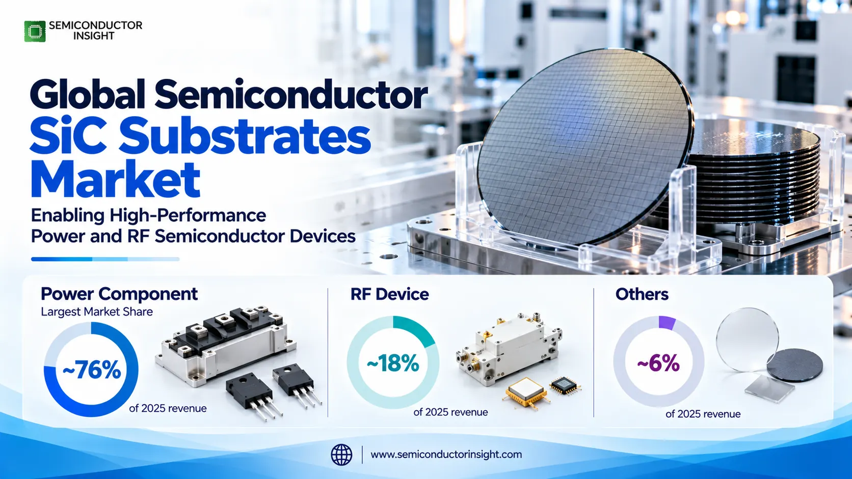
- Device destination: Power Component accounts for an estimated ~76% of base-year substrate sales, whereas RF Device is a smaller but strategically distinct application using different resistivity and qualification requirements.
- Regional structure: Asia-Pacific holds an estimated ~49% of global 2025 sales, reflecting Chinese crystal-growing operations, Japanese power-device supply chains, Korean materials investment and manufacturing demand in Southeast Asia.
- Growth mechanisms: Electric-vehicle power conversion, wafer-diameter migration, industrial electrification and resilient multi-source purchasing create incremental demand; defects, costly crystal growth and long customer approval cycles constrain realized revenue.
Global Semiconductor SiC Substrates Market Overview
Semiconductor SiC substrates market was valued at USD 1,883.75 million in 2025, is estimated at USD 2,124.86 million in 2026 and is projected to reach USD 5,569.12 million by 2034, representing a 12.8% CAGR over 2026–2034. Asia-Pacific is the largest region with an estimated ~49% share in 2025; the 6 Inches category is the principal qualified production platform.
Silicon carbide substrates are polished crystalline starting wafers that carry the active device layers of wide-bandgap semiconductor components. They are not the transistors, rectifiers or inverter assemblies sold to end users. Producing a substrate requires controlled crystal growth, ingot orientation, wafer slicing, grinding, polishing and defect inspection before an epitaxial layer can be deposited by the downstream manufacturer. Yield at each of those stages affects the material supplier’s ability to supply uniform commercial lots.
The market boundary includes bare semiconductor-grade SiC wafers and engineered bonded substrates purchased for device fabrication. Conductive material is primarily associated with power MOSFETs and Schottky diodes; semi-insulating grades are used where radio-frequency device isolation matters. Separately billed epitaxial services, fabrication equipment, finished chips, power modules and traction inverters remain outside substrate revenue. The distinction prevents counting one wafer repeatedly as it moves through increasingly expensive manufacturing stages.
The transition from 150 mm to 200 mm wafer processing is a structural development rather than an immediate replacement of all installed equipment. A larger diameter offers more geometric surface area, but usable die output depends on defect density, edge exclusion, wafer bow, thickness uniformity and process compatibility. Manufacturers therefore qualify crystal quality and downstream epitaxy together, while maintaining established 150 mm production where process yields and customer designs are already proven.
Crystal-growth economics differ from those of silicon wafers. SiC boules require demanding high-temperature processing and defect management, and each subsequent finishing step can reject material that has already absorbed significant production cost. Long customer approvals reward consistent crystallographic orientation, doping, resistivity and surface preparation. Premium product pricing can therefore reflect reliability and repeatability rather than wafer diameter alone, particularly for high-voltage devices with sensitive breakdown characteristics.
Demand is ultimately derived from power-electronics production in electric vehicles, charging infrastructure, renewable generation, industrial drives and power supplies, together with specialist RF electronics. The same end-market activity should not be interpreted as substrate sales: vehicle shipments, fab investment and device announcements establish direction and potential customer capacity, not a directly measured value for bare wafers. Material revenue depends on wafer starts, accepted substrate yield and contracted selling prices.
The annual trajectory implied by the two headline anchors places modeled market value at USD 2,396.83 million for 2027, USD 2,703.61 million for 2028, USD 3,049.66 million for 2029, USD 3,440.00 million for 2030, USD 3,880.30 million for 2031, USD 4,376.96 million for 2032 and USD 4,937.19 million for 2033. On an index with 2026 equal to 100.0, successive year-end levels are 112.8, 127.2, 143.5, 161.9, 182.6, 206.0, 232.4 and 262.1 through 2034. This index illustrates the compounding path and does not represent independently measured annual sales.
Segment Analysis: By Type
By type, the published categories are 4 Inches, 6 Inches and Others. The 6 Inches class holds an estimated ~62% of 2025 substrate revenue because 150 mm fabrication is widely qualified, while Others has an estimated ~27% share and includes the transition toward 200 mm products. Four-inch wafers retain a smaller estimated ~11% position in specialist and legacy programs.
| Type | Technology and customer role | Market positioning |
|---|---|---|
| 4 Inches | Four-inch wafers support mature qualification programs, selected RF device work, university and industrial research, and fabrication lines that have not justified a major diameter conversion. Buyers may accept smaller batch sizes in exchange for stable device parameters and continued availability. The category also supports development activity where process equipment is configured around the older substrate format. | An estimated ~11% of 2025 value remains associated with 100 mm material, and its commercial character differs from the newer diameter platforms. Pricing is often shaped by specialized resistivity, crystal orientation and smaller production runs rather than scale. Customers prioritize continuity of approved material and process recipes, so the segment can persist even when the wider industry invests in larger wafers. |
| 6 Inches | Six-inch substrates form the established production base for many conductive SiC power devices and semi-insulating RF structures. A 150 mm wafer combines a large enough die field for volume processing with well-understood polishing, metrology and epitaxy recipes. The format is supported by existing furnaces, implant tools, lithography equipment and packaging designs, reducing changeover risk for qualified automotive programs. | The leading type represents an estimated ~62% of base-year revenue, with modeled growth of ~11.8% annually. Its dominance reflects installed production rather than a claim that 150 mm has the best theoretical economics. Suppliers can defend contracts through low defect density, lot traceability and predictable surface characteristics even as large customers establish parallel 200 mm qualification lines. |
| Others | The residual category contains diameters not individually identified in the publisher segmentation, including commercially developing 200 mm wafers and larger exploratory platforms. The transition is material-intensive because an increase in diameter magnifies crystal-growth, wafer-shape and finishing challenges. Customer acceptance also requires matching epitaxial uniformity and device yield, not merely producing an intact larger disk. | An estimated ~27% of 2025 value is allocated to Others, with modeled growth near ~16.6% as 200 mm commercial programs scale. This is an analytical allocation across the publisher’s residual type, not a measured standalone 8-inch market share. Advanced thermal-management sampling on 300 mm platforms is a related materials development and should not be counted automatically as power-device substrate shipments. |
How wafer diameter changes purchasing economics
A transition from 100 mm through 150 mm to 200 mm changes both potential die count and the manufacturing steps needed to realize it. Substrate acceptance is determined by more than nominal diameter: incoming defect maps, usable surface, thickness tolerance and epitaxial compatibility all affect the cost of good devices. The strongest commercial case arises when material supply, process equipment and customer product design mature together.
The published 4 Inches, 6 Inches and Others groups are retained without adding a separate fourth type. The larger-diameter transition is discussed inside Others, preserving the original segmentation while distinguishing mature 150 mm procurement from newer 200 mm qualification. That treatment avoids assigning an unsupported standalone market percentage to a size that the publisher did not isolate.
Segment Analysis: By Application
The application segmentation comprises Power Component, RF Device and Others. Power Component is the largest with an estimated ~76% share of 2025 revenue, supported by traction inverters and high-efficiency industrial conversion; RF Device represents an estimated ~18%, while the residual applications group accounts for ~6% and is treated separately from the primary power-device demand stream.
| Application | Demand characteristics |
|---|---|
| Power Component | Conductive substrates underpin SiC MOSFETs, Schottky rectifiers and related power devices used in automotive, charging, renewable-energy and industrial systems. Customers specify doping, resistivity, basal-plane defect behavior and surface quality because these properties affect device reliability and manufacturing yield. The application holds an estimated ~76% share, but end-system equipment revenue is not included in this material-only category. |
| RF Device | Radio-frequency applications use substrate properties suited to high-frequency amplification and isolation, often emphasizing semi-insulating material and low parasitic loss. Telecom infrastructure and selected aerospace electronics create demand that is smaller than the power-device stream but technically demanding. An estimated ~18% revenue allocation reflects specialized qualification and performance requirements, not a claim about the number of installed base stations. |
| Others | The remaining estimated ~6% includes specialist semiconductor development, emerging device architectures and qualified niche material programs that do not fit the two principal customer categories. Applications are heterogeneous, so a single growth assumption should not be mistaken for a uniform demand curve. Commercial value depends on whether exploratory material programs advance into repeatable orders with clear acceptance specifications. |
The application split also separates different qualification economics. Power-device producers optimize for blocking voltage, conduction loss and switching behavior across large manufacturing lots, whereas RF users may attach greater value to electrical isolation and microwave performance. These requirements influence crystal grade, polishing and testing, so substrate producers can operate several product families even when they share crystal-growth infrastructure and a common silicon carbide materials platform.
Regional Analysis
Asia-Pacific is the leading region with an estimated ~49% of global 2025 substrate revenue and modeled ~13.7% CAGR. North America follows at ~22% and ~11.7% CAGR, Europe at ~20% and ~12.2%, South America at ~5% and ~11.9%, and Middle East & Africa at ~4% and ~11.2%. These allocations describe a modeled commercial market, not an official country-level supplier census.
Which regional supply and customer patterns shape SiC substrate demand?
The location where a substrate is grown is not necessarily the location where the finished power device is sold. Asia-Pacific combines crystal growers, device makers and major manufacturing investments, while North America maintains important crystal technology and merchant wafer capacity. European device manufacturers have strong reasons to secure long-term material supply and regional manufacturing capability. Emerging regions mainly influence upstream wafer demand through downstream electricity infrastructure and imported power-conversion equipment rather than domestic SiC crystal production.
| Region | Position | Growth outlook | Demand profile | What decides supplier selection |
|---|---|---|---|---|
| Asia-Pacific | Largest (~49%) | ~13.7% CAGR | China, Japan, Korea and Malaysia | Crystal quality, qualified supply volume and fabrication transition readiness |
| North America | Second (~22%) | ~11.7% CAGR | U.S. crystal-growth expertise | Defect maps, long-term sourcing and automotive-grade consistency |
| Europe | Third (~20%) | ~12.2% CAGR | Power-device manufacturing and materials engineering | Integrated production programs and wafer qualification |
| South America | Smaller (~5%) | ~11.9% CAGR | Downstream power conversion | Imported device content and project economics |
| Middle East & Africa | Smaller (~4%) | ~11.2% CAGR | Renewable and utility conversion | Supplier reliability and systems procurement |
Global Semiconductor SiC Substrates Market Competitive Landscape
Competitive positioning in SiC substrates is determined by crystal-growth expertise, qualified wafer diameter, electrical grade, surface finishing and long-term delivery performance. Merchant substrate producers compete with integrated semiconductor groups and engineered-wafer specialists, and these business models should not be combined into a single ranking based on consolidated company revenue. Historical supplier names are reconciled with their current corporate identities.
Wolfspeed retains a significant materials identity that predates the separation of the former Cree business, while Coherent represents the company previously known as II-VI. STMicroelectronics acquired Norstel, and ROHM’s SiCrystal business supplies another example of integration between material and power-device operations. These ownership distinctions matter because a materials producer can supply external customers, internal fabs or both, and the reported company revenue is not a pure measure of substrate merchant sales.
Asian suppliers including SK Siltron, SICC Materials and TankeBlue participate in a competitive landscape shaped by customer qualification and increasing domestic supply capabilities. Some names appearing in historical publisher company lists may reflect older branding or require further verification before a present-day market-share claim can be made. No specific company percentage is assigned here because product revenue disclosures are not comparable across merchant wafers, captive substrate transfers and finished power devices.
The primary commercial differentiator is consistent yield after epitaxy and fabrication, not the diameter label on a product catalogue. Buyers evaluate micropipes, threading dislocations, basal-plane defects, resistivity distribution, flatness and surface damage because poor incoming quality can undermine several subsequent expensive processing stages. Qualification records and lot traceability can therefore outweigh a modest purchase-price advantage when devices are destined for automotive or high-reliability industrial service.
Capacity announcements require careful interpretation. A new crystal-growth line, a polishing expansion and a semiconductor device fab each describe different points in the value chain; none can be substituted mechanically for annual accepted wafer shipments. In 200 mm programs, usable wafer yield, stable processing recipes and repeat customer orders will determine whether the commercial market shifts from development batches to sustained high-volume material revenue.
Tier structure
| Tier | Companies | Basis of competition |
|---|---|---|
| Established materials leaders | Wolfspeed; Coherent; SK Siltron | Large-scale materials capabilities and technical relationships across wafer growth, finishing and customer qualification |
| Integrated device-material groups | STMicroelectronics/Norstel; ROHM/SiCrystal; Resonac | Supply decisions connect crystal operations to internal power-device manufacturing and external customer opportunities |
| Specialist and developing suppliers | SICC Materials; TankeBlue; Soitec; other qualified crystal producers | Compete through material grade, engineered-wafer architecture, production consistency and specific customer approvals |
Key companies profiled
- Wolfspeed
- Coherent
- SK Siltron
- SICC Materials
- TankeBlue
- STMicroelectronics
- ROHM
- SiCrystal
- Soitec
- Resonac
- Tokai Carbon
- Mitsubishi Electric
Semiconductor SiC Substrate Manufacturing and Production Economics
A substrate is a high-value input long before device lithography begins. Production starts with crystalline material growth and continues through ingot preparation, wafering, edge shaping, grinding, chemical-mechanical polishing, inspection and final acceptance. The economics are sensitive to how much of the grown boule survives each step and whether the resulting surface supports the customer’s epitaxial process.
Physical vapor transport and related crystal-growth methods must control thermal gradients, doping and crystallographic defects over extended processing cycles. A boule with apparently useful volume can lose substantial commercial value if defect density or electrical nonuniformity limits the number of accepted wafers. Crystal growth also creates capital and energy commitments before the manufacturer knows how many polished wafers will satisfy a particular customer specification.
Wafer slicing and polishing introduce their own yield challenges. Kerf losses reduce usable material, while wafer bow, warp, surface roughness and subsurface damage can impair epitaxial uniformity or tool handling. As diameter increases, these geometric tolerances become harder to maintain across the full surface. Incoming inspection and wafer mapping are therefore integral to product qualification rather than optional quality-control expenses.
Electrical grade is a second important manufacturing distinction. Conductive n-type substrates support many power-device structures, whereas semi-insulating wafers serve selected radio-frequency architectures. A supplier cannot assume that material suitable for one grade will meet the other customer’s resistivity and defect criteria. This is why application revenue should be modeled separately even when some factories share upstream equipment and finishing operations.
Engineered bonded wafers introduce a different pathway. A high-quality crystalline donor layer can be transferred onto a lower-resistivity support wafer, potentially improving material utilization and device characteristics. Commercial adoption nevertheless depends on bonding integrity, thermal behavior, device robustness and compatibility with established fab recipes. The process may change the balance between bulk crystal cost and finishing complexity without removing the need for rigorous qualification.
Semiconductor SiC Substrates Market Dynamics: Drivers, Restraints and Opportunities
Demand for semiconductor-grade silicon carbide wafers expands as more power-device manufacturers qualify the material for electric mobility, grid conversion and industrial efficiency. The central investment decision is whether improved electrical performance justifies the cost and yield risk of SiC processing. Supplier economics also depend on the speed of 200 mm conversion and the ability to turn technical wafer availability into repeatable commercial orders.
MARKET DRIVERS
Drivers Impact Analysis*
| Market Drivers | Impact Rank | CAGR Contribution (%) | 2026–2028 | 2029–2031 | 2032–2034 |
|---|---|---|---|---|---|
| Electric-vehicle power electronics substrate demand | High | +5.10% | High | High | Medium |
| 200 mm transition and wafer-area economics | High | +3.80% | Medium | High | High |
| Renewable and industrial power conversion | Medium-High | +2.70% | Medium | High | High |
| Customer qualification and resilient multisourcing | Medium | +2.10% | High | Medium | Medium |
| RF and other wide-bandgap electronics | Low-Medium | +1.50% | Medium | Medium | Medium |
| Others (engineered wafers and specialty high-voltage programs) | Low | +0.90% | Low | Medium | High |
Electrified vehicles increase qualified device demand
Electric traction inverters, onboard chargers and high-efficiency DC/DC systems are important demand channels for SiC power devices. Vehicle production does not translate one-for-one into substrate revenue, because semiconductor architecture, device area and fabrication yield vary by model and supplier. Nonetheless, sustained adoption can justify multi-year material procurement commitments and create a predictable baseline of wafer starts for qualified substrate manufacturers.
Larger diameters alter the cost curve
Moving from 150 mm to 200 mm substrates offers a greater usable surface per wafer when crystal quality and downstream processing yield remain controlled. The transition requires new tooling, process development and incoming-wafer acceptance, so commercial benefits appear unevenly across customers. Material producers with consistent 200 mm crystal growth can gain strategic positions before the full device manufacturing ecosystem completes its conversion.
Industrial and grid conversion broaden the demand base
Renewable-energy inverters, charging stations, industrial drives and power supplies can use SiC to reduce switching losses and manage heat in selected voltage and power ranges. Adoption is driven by total system efficiency rather than substrate pricing in isolation. For material vendors, diversification beyond automotive reduces exposure to one end market while increasing the variety of device structures and customer qualification specifications.
Supplier diversification becomes a procurement priority
A manufacturer dependent on a single high-purity crystal supplier faces disruption risk when production yields fluctuate or expansion schedules slip. Dual sourcing requires equivalence testing across resistivity, defects and wafer geometry, but it can improve delivery resilience once completed. Long-term material contracts and qualification support can become competitive advantages for suppliers that demonstrate stable output across multiple device fabs.
MARKET RESTRAINTS
Restraints Impact Analysis*
| Market Restraints | Impact Rank | CAGR Contribution (%) | 2026–2028 | 2029–2031 | 2032–2034 |
|---|---|---|---|---|---|
| Crystal defects and yield variability | High | -1.40% | High | High | Medium |
| Crystal-growth and finishing capital intensity | Medium-High | -0.90% | High | Medium | Medium |
| Lengthy device-customer qualification cycles | Medium | -0.60% | High | Medium | Low |
| Others (substitution, inventory cycles and price pressure) | Low | -0.40% | Medium | Low | Low |
Defects can destroy downstream device value
Micropipes, threading dislocations and surface imperfections can compromise epitaxy or the electrical behavior of fabricated devices. A rejected substrate has already absorbed crystal-growth and finishing cost, while a defect detected later may also waste expensive device processing. These risks make incoming inspection and consistent material quality critical and can limit the pace at which new diameter platforms achieve acceptable production economics.
Large-diameter capacity is expensive to qualify
Crystal-growth furnaces, wafering tools, polishing equipment and metrology systems require substantial investment, while larger wafers impose tighter geometric control across more surface area. New capacity may run below its nominal output during process learning. Suppliers must fund the transition before all customers are ready to purchase high volumes, creating a period when utilization and cash generation can lag technical progress.
Customer approvals slow commercial conversion
Power-semiconductor makers do not replace an established substrate source simply because a new wafer is physically available. Qualification may require epitaxial evaluation, electrical tests, device reliability evidence and repeated production lots. Automotive-grade programs add demanding traceability and change-control requirements. The resulting lead time separates development announcements from booked substrate sales and can postpone revenue even where long-term customer interest is strong.
Alternative technologies influence device architecture
Conventional silicon remains economical for many power applications, and gallium nitride offers advantages in selected lower-voltage, high-frequency systems. Even when SiC is technically attractive, device manufacturers and equipment designers must balance efficiency against manufacturing cost and qualification burden. Inventory corrections and aggressive pricing can further weaken short-term substrate revenue without changing the longer-run case for wide-bandgap electronics.
MARKET OPPORTUNITIES
Premium defect-controlled 200 mm material
Customers moving to 200 mm fabrication need starting wafers with consistent electrical properties and tight geometric tolerances, creating room for differentiated premium products. Suppliers that can demonstrate low micropipe counts and stable lot quality may gain share even if their quoted wafer prices are not the lowest. Commercial success depends on the customer’s accepted-device yield and repeat orders rather than isolated laboratory records.
Engineered wafers create another design option
Bonded and reusable-donor substrate architectures can offer a route to lower resistance or improved use of high-quality single crystal material. Such approaches may appeal to device manufacturers facing cost and performance tradeoffs at larger diameters. Validation in particular diode and MOSFET processes is a meaningful milestone, although each additional fab and voltage class still requires its own reliability and integration work.
High-voltage applications reward material consistency
Power systems requiring higher blocking voltage can increase the value of carefully controlled SiC material and compatible thick epitaxial structures. The substrate supplier’s role is to provide low-defect starting wafers that support downstream device yield. Opportunities are likely to be specialized initially, because higher-voltage design changes device architecture and processing rather than merely increasing the number of conventional wafers purchased.
New materials applications may diversify capacity
Thermal-management uses of large-diameter silicon carbide could eventually broaden the addressable product mix for crystal growers and polishers. These developments remain adjacent to the present power-semiconductor substrate boundary where they target heat spreading rather than active power devices. Their strategic significance lies in potentially sharing manufacturing expertise, while their revenue must be separated from core conductive and semi-insulating device-wafer sales.
Semiconductor SiC Substrate Supply Chain Analysis
The value chain connects high-purity source materials and crystal-growth equipment to ingot production, wafer slicing, finishing, characterization and device-fab qualification. A finished substrate can be sold to a merchant epitaxy supplier, transferred within an integrated semiconductor company or delivered directly to a power-device manufacturer. Each route has different contractual and revenue-recognition implications.
Upstream materials. Source purity, growth conditions and doping control influence the defect and resistivity profile of a SiC boule. Equipment reliability matters because high-temperature crystal growth is energy intensive and long process cycles amplify losses when material falls outside specification. Suppliers with stable growth recipes can reduce variability before wafering begins, making upstream process knowledge an important determinant of commercial material yield.
Wafer conversion. After crystal growth, slicing and finishing convert an ingot into individual substrates that must meet dimensional and surface requirements. Thickness, flatness, warp and polishing damage influence whether the wafer can pass downstream epitaxial processing. A producer that expands nominal boule output without sufficient high-quality finishing capacity may not increase saleable wafer deliveries by the same proportion.
Customer qualification. Device manufacturers compare incoming substrates with established material specifications and test how they behave after epitaxy and fabrication. Electrical and structural measurements are combined with reliability evidence from representative devices. Approval is usually tied to specific processes and product families, so a wafer qualified at one fab cannot automatically be assumed to have identical commercial acceptance across all customers.
Commercial channels. Independent material suppliers sell bare wafers under contracts that may include technical support and delivery commitments, while integrated manufacturers can transfer substrates internally. Engineered-wafer specialists add bonding and donor-material reuse to the supply structure. Separating these channels prevents a consolidated semiconductor company’s finished-device sales from being counted again as substrate revenue and clarifies which purchases are genuinely accessible to merchant suppliers.
Recent Developments in Semiconductor SiC Substrates
- 15 October 2026 Agreement
Infineon and Wolfspeed announced a multi-year supply arrangement extending their silicon carbide wafer relationship to 200 mm material. The agreement supports Infineon’s conversion from 150 mm processing and strengthens its supplier diversification strategy. It is direct evidence of substrate procurement planning, but the announcement does not disclose a separate market-wide wafer revenue figure or completed delivery volumes. Source - 27 September 2026 Product
Wolfspeed introduced a commercially available premium 200 mm n-type silicon carbide substrate focused on lower defects and improved wafer-shape stability. The company reported fewer than 0.01 micropipes per square centimeter for the product. This is a materials-quality milestone relevant to high-yield device fabrication; it should not be interpreted as a published estimate of global substrate market share. Source - 17 August 2026 Sampling
Coherent began customer sampling of 300 mm high-thermal-conductivity silicon carbide substrates for artificial-intelligence infrastructure. The development demonstrates a possible extension of SiC crystal and polishing capabilities into advanced heat-spreading applications. It is classified as adjacent materials activity because the announced samples target thermal management, not a verified high-volume power-semiconductor device-wafer revenue stream. Source - 9 April 2026 Technology
Coherent announced advances in thick SiC epitaxial wafer capability for devices targeting up to 10 kV operation. The technical direction highlights why low-defect starting substrates and compatible epitaxy are important for high-voltage device development. Epitaxial processing is a separate value-chain activity, so this announcement is relevant demand and technology evidence rather than a direct measurement of bare-substrate sales. Source - 13 January 2026 Milestone
Wolfspeed disclosed a 300 mm silicon carbide single-crystal technology milestone, extending its materials development beyond established production diameters. Producing a large crystal is not equivalent to qualifying a complete commercial device manufacturing flow, because wafering, polishing, epitaxy and customer process compatibility remain necessary. The announcement indicates a possible future technology direction without establishing current 300 mm power-wafer market revenue. Source - 3 December 2025 Platform
Coherent described a 300 mm SiC development platform associated with thermal management and future semiconductor applications. The larger diameter could extend material expertise to additional customers, but production and application readiness differ by use case. AI packaging and heat-spreading demand are therefore kept distinct from the present market’s conductive and semi-insulating substrates sold for active power and RF device fabrication. Source - 27 November 2025 Validation
Soitec and Diodes reported validation of 150 mm SmartSiC engineered substrates for SiC power devices, including tests involving 650 V diodes and 1,200 V MOSFET structures. The announcement provides evidence that bonded substrate architecture can meet specific device requirements. Qualification at these product nodes is meaningful but does not imply automatic adoption by every semiconductor manufacturer or universal substitution of bulk SiC wafers. Source - 10 September 2025 Commercial
Wolfspeed announced the commercial launch of its 200 mm SiC materials portfolio, including bare substrates and epitaxial wafers available for qualification. The release established an important availability milestone for customers preparing larger-diameter fabrication. Substrate and epitaxy products are separate revenue objects, so only the bare or engineered starting-wafer portion belongs in the substrate market boundary used here. Source
REPORT SCOPE & SEGMENTATION
| Attribute | Details |
|---|---|
| Study Period | 2020–2034 |
| Base Year | 2025 |
| Estimated Year | 2026 |
| Forecast Period | 2026–2034 |
| Historical Period | 2020–2024 |
| Market Size 2025 | USD 1,883.75 million |
| Market Size 2026 | USD 2,124.86 million |
| Market Size 2034 | USD 5,569.12 million |
| Growth Rate | CAGR of 12.8% from 2026–2034 |
| Unit | Revenue (USD million) |
| Segmentation | By Type, By Application and By Region |
| By Type | 4 Inches · 6 Inches · Others |
| By Application | Power Component · RF Device · Others |
| By Region | Five regions are evaluated by Type, Application and Country, with modeled 2025 revenue shares. North AmericaUnited States, Canada, Mexico EuropeGermany, France, Italy, Rest of Europe Asia-PacificChina, Japan, South Korea, Malaysia, Rest of Asia-Pacific South AmericaBrazil, Argentina, Rest of South America Middle East & AfricaSaudi Arabia, United Arab Emirates, South Africa, Rest of Middle East & Africa |
| Key Companies Profiled | Wolfspeed, Coherent, SK Siltron, SICC Materials, TankeBlue, STMicroelectronics, ROHM, SiCrystal, Soitec, Resonac, Tokai Carbon, Mitsubishi Electric |
| Customization Scope | Country-level material qualification, wafer-diameter mix and application scope can be customized for purchasing organizations. |
Frequently Asked Questions
How large is the global semiconductor SiC substrates market?
The global market is valued at USD 1,883.75 million in 2025 and is estimated at USD 2,124.86 million for 2026, with a 2034 projection of USD 5,569.12 million. The 2026–2034 CAGR is 12.8%. The figures concern semiconductor-grade starting substrates, not the much larger combined revenue of finished power devices, inverters or other downstream equipment.
What does a silicon carbide substrate supplier actually sell?
A supplier provides a polished crystalline wafer that meets specified electrical, geometric and defect requirements for subsequent semiconductor processing. Products can be conductive or semi-insulating, and some are engineered bonded wafers. Epitaxial growth may be sold by the same business, but when it is billed separately that added processing is outside the bare-substrate revenue boundary considered here.
Which wafer sizes are included in the type segmentation?
The publisher divides the market into 4 Inches, 6 Inches and Others. The 6 Inches category is the largest at an estimated ~62% of 2025 revenue, while Others includes larger diameters such as 200 mm products. That classification deliberately retains the publisher’s residual bucket rather than inventing a standalone share for 8-inch material that was not separately disclosed.
Why are power components the leading application?
Conductive SiC substrates support power MOSFETs and rectifiers used in traction systems, industrial conversion, charging and renewable-energy equipment. Those applications create repeated wafer demand when device makers qualify a process and begin volume production. The Power Component category holds an estimated ~76% of the modeled 2025 application mix, while RF and specialist applications use different electrical material specifications.
Which region has the largest substrate market share?
Asia-Pacific leads with an estimated ~49% share in 2025 because it combines crystal-growing operations, device manufacturing, major customers and new wafer-processing investments. China, Japan, South Korea and Malaysia contribute through different parts of the value chain. The percentage is a modeled revenue allocation, not a directly reported share from a single industry association or company filing.
Who are the important companies in SiC substrates?
Relevant companies include Wolfspeed, Coherent, SK Siltron, SICC Materials, TankeBlue, STMicroelectronics, ROHM and its SiCrystal business, and engineered-wafer specialist Soitec. Their business models differ substantially: some sell merchant material, some use substrates internally and others specialize in bonded structures. Consolidated corporate revenue should therefore not be treated as a comparable measure of bare-wafer market share.
Why does 200 mm wafer conversion matter commercially?
A 200 mm wafer offers more potential device area than a 150 mm wafer, but its benefit depends on acceptable crystal defects, surface quality, epitaxy and downstream fab yields. Customers need new qualification work and sometimes different equipment. Successful conversion can improve unit economics and support supply agreements, while poor yield can offset the geometric advantage of a larger starting wafer.
What is the main production challenge for SiC substrates?
Crystal defects and geometric consistency are central challenges because material failures can be discovered after expensive growth, slicing or device processing. Micropipes, dislocations, bow and polishing damage influence whether a wafer is usable for a particular design. Suppliers must also maintain electrical resistivity and lot traceability across production batches, making repeatable accepted yield more important than nominal crystal-growth capacity alone.
How do power-device and RF-device substrate grades differ?
Power applications generally use conductive material selected for the required device structure and current path, while many RF applications rely on semi-insulating substrates to limit parasitic effects. The manufacturing and qualification targets therefore differ even though both materials are silicon carbide. A wafer accepted by a power MOSFET producer cannot automatically be assumed suitable for a high-frequency RF process without additional electrical testing.
What years and products does the market outlook cover?
The study uses 2025 as its base year, 2026 as the estimated year and 2026–2034 as the forward period, with historical context from 2020–2024. It covers semiconductor-grade bare and engineered SiC substrates by the publisher’s type and application axes across five world regions. Finished semiconductor devices, complete inverters and separately charged epitaxial services are excluded to avoid overlapping revenue.
Research Sources & Evidence Base
Get Sample Report PDF for Exclusive Insights
Report Sample Includes
- Table of Contents
- List of Tables & Figures
- Charts, Research Methodology, and more...
 Download Sample Report PDF