
Key Statistics
Key Takeaways
- Metal precursors are gaining strategic importance as advanced logic and memory explore molybdenum, ruthenium, cobalt and other metals for contacts, interconnects and electrodes.
- PVD/CVD/ALD is the largest application group because thin-film deposition is the core use case for semiconductor precursors across logic, memory and advanced packaging.
- Asia Pacific leads the market through the concentration of semiconductor fabs and materials manufacturing in South Korea, Taiwan, Japan and China.
- Atomic layer deposition is a major structural growth mechanism because shrinking features and 3D structures require conformal films with atomic-scale thickness control.
- Purity and delivery systems are critical competitive factors. Precursor chemistry must remain stable from synthesis through storage, vapor delivery and deposition without introducing metallic or particulate contamination.
- Molybdenum is a major current innovation area. Air Liquide started a large-scale molybdenum advanced-materials plant in South Korea in 2025, while Entegris supplies high-purity MoO2Cl2 for logic, DRAM and 3D NAND.
Precursor for Semiconductor Market Overview
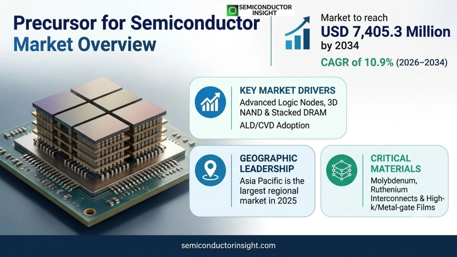
Semiconductor Precursor Market was valued at USD 2,918.5 million in 2025, is estimated at USD 3,236.6 million in 2026, and is projected to reach USD 7,405.3 million by 2034, representing a CAGR of 10.9% during 2026–2034. Asia Pacific is the largest regional market in 2025, while the commercial growth mechanism is increasingly shaped by advanced logic nodes, 3D NAND and stacked DRAM, ALD/CVD adoption, molybdenum and ruthenium interconnects, high-k/metal-gate films, compound semiconductors, and regional fab expansion.
Semiconductor precursors are ultra-high-purity chemical compounds that carry target elements into deposition, epitaxy, etch and related wafer processes. They can be gases, liquids or volatile solids and are selected for controlled vapor pressure, thermal stability, reactivity and film properties. Major groups include silicon, metal, high-k and low-k precursors used in atomic layer deposition, chemical vapor deposition and other thin-film processes.
Advanced device scaling is increasing the number and complexity of deposited films. Gate-all-around transistors, 3D NAND, stacked DRAM, chiplets and new interconnect metals require conformal layers inside narrow trenches, vias and high-aspect-ratio structures. This favors ALD and advanced CVD chemistries that can deliver uniform films at lower temperature and with tightly controlled impurities.
The market has high barriers because a precursor is not interchangeable like a commodity chemical. Suppliers work with chipmakers and deposition-equipment companies to co-develop chemistry, delivery hardware and process windows. Once qualified, the material must be manufactured at semiconductor-grade purity with highly consistent composition across batches and secure local supply near customer fabs.
Segment Analysis: By Type
By type, the market is segmented into Silicon Precursor, Metal Precursor, High-k Precursor, and Low-k Precursor. Silicon precursors remain foundational across dielectric and nitride deposition, while metal precursors are the most dynamic strategic category as advanced devices adopt new conductor and contact materials.
| Type | Technical role | Market position |
|---|---|---|
| Silicon Precursor | Includes silanes and chlorosilanes used to deposit silicon-containing dielectrics, nitrides, oxides and related films through CVD, ALD and LPCVD processes. | A foundational high-volume category used throughout semiconductor manufacturing. Growth follows 3D NAND layer count, gate stacks and low-temperature film requirements. |
| Metal Precursor | Includes titanium, hafnium, tantalum, tungsten, molybdenum, cobalt, ruthenium and other metal-organic or halide chemistries used for conductors, barriers, electrodes and high-k integration. | The most dynamic strategic segment. New interconnect and gate materials can create rapid qualification demand and premium pricing for high-purity molecules. |
| High-k Precursor | Used to deposit high-permittivity dielectric films such as hafnium-based materials in advanced logic and memory capacitors. | A premium segment linked to gate-all-around logic, DRAM capacitors and advanced transistor scaling. |
| Low-k Precursor | Used to create low-dielectric-constant films that reduce parasitic capacitance in interconnect stacks. | A mature but important segment where process integration, mechanical strength and low-temperature deposition remain critical. |
Why do new device architectures require more specialized precursor chemistry?
Planar structures could tolerate line-of-sight or less conformal deposition in many steps. Gate-all-around logic, 3D NAND and stacked structures contain deep, narrow and three-dimensional features that require uniform film thickness over complex surfaces. A suitable precursor must volatilize cleanly, react selectively and leave minimal carbon, chlorine or metallic residue. As dimensions shrink, small changes in purity or reaction kinetics can materially affect yield, so material design becomes part of device integration.
Segment Analysis: By Application
By application, the report segments the market into PVD/CVD/ALD and Epitaxial Growth and Etching, etc. PVD/CVD/ALD is the leading application group because precursors are core feed materials for thin-film deposition across logic, memory and advanced packaging.
| Application | Demand characteristics | |
|---|---|---|
| PVD/CVD/ALD | Precursors deliver silicon, metals, dielectrics and dopants during chemical and atomic-layer deposition. ALD is especially important for conformal films and atomic-scale thickness control. | The largest application group and the primary source of market growth as advanced nodes and 3D memory add more deposition steps. |
| Epitaxial Growth and Etching, etc. | Specialty gases and organometallic compounds support epitaxy, selective growth, etch, doping and cleaning processes for silicon and compound semiconductors. | A significant complementary segment tied to SiC, GaN, advanced logic and specialized material systems. |
Why is ALD particularly important to market growth?
ALD deposits material through self-limiting surface reactions, allowing highly conformal films across complex three-dimensional structures. As device dimensions shrink and 3D NAND layer counts increase, the ability to control film thickness at the atomic scale becomes more valuable. Entegris develops application-specific ALD/CVD precursor portfolios, while suppliers increasingly pair chemistry with delivery systems that maintain purity and stable vapor flow from container to wafer.
Regional Analysis
Asia Pacific leads the Precursor for Semiconductor market because South Korea, Taiwan, Japan and China contain the largest concentration of wafer-fab capacity and a dense advanced-materials supply chain. North America is expanding through domestic fab and materials investment, while Europe combines leading chemical suppliers with specialized semiconductor manufacturing.
How do regional precursor markets differ?
Asia Pacific combines the largest consumption base with significant local precursor manufacturing and customer co-development. North America is driven by advanced logic, memory and fab regionalization. Europe has strong specialty-chemical capability and global materials companies. South America has limited direct wafer-fab demand, while Middle East and Africa remain early-stage semiconductor manufacturing markets.
| Region | Position | Growth outlook | Demand profile | What decides supplier selection |
|---|---|---|---|---|
| Asia Pacific | Largest | Very strong | Logic, memory and materials manufacturing | Ultra-high purity, local supply and rapid qualification |
| North America | Strategic expansion market | Strong | Advanced logic, memory and onshoring | Domestic supply, process collaboration and safety |
| Europe | Materials & specialty semiconductor market | Moderate to strong | Chemical innovation, power and R&D | Purity, regulation and global customer support |
| South America | Early-stage direct market | Selective | Research and limited semiconductor manufacturing | Cost, import availability and local technical support |
| Middle East & Africa | Emerging strategic market | Long-term | Pilot fabs and technology diversification | Partnerships, logistics and safety infrastructure |
Competitive Landscape
The market includes Merck, Air Liquide, SK Materials, UP Chemical, Entegris, ADEKA, Hansol Chemical, DuPont, Soulbrain, Nanmat, DNF Solutions, Natachem, Tanaka Kikinzoku, Botai Electronic Material, Gelest, Strem Chemicals, Anhui Adchem, EpiValence, Fujifilm, Japan Advanced Chemicals and Wonik Materials.
Air Liquide, Merck and Entegris compete through broad portfolios, global customer relationships and the ability to combine chemical development with high-volume manufacturing and delivery systems. Air Liquide’s Subleem molybdenum initiative shows how a supplier can commercialize a new material through molecule design and proprietary distribution hardware.
Entegris differentiates through application-specific ALD/CVD precursors, advanced delivery systems and contamination control. Its Korea Technology Center adds local precursor synthesis and ALD capability close to major memory customers. Japanese suppliers such as ADEKA, Fujifilm and Tanaka bring deep specialty-chemical and purity expertise.
Korean suppliers including SK Materials, UP Chemical, Hansol, Soulbrain, DNF and Wonik benefit from proximity to major DRAM, HBM and NAND manufacturers. Local customer access is a major advantage because precursor qualification often requires repeated process tuning and rapid analytical support.
| Competitive tier | Representative companies | Commercial basis |
|---|---|---|
| Global advanced-materials leaders | Merck; Air Liquide; Entegris; DuPont; Fujifilm | Broad precursor portfolios, global supply, R&D, purity control and delivery systems. |
| Korean semiconductor-materials specialists | SK Materials; UP Chemical; Hansol Chemical; Soulbrain; DNF Solutions; Wonik Materials | Close memory-fab relationships, local high-volume supply and rapid process support. |
| Japanese & specialty chemistry suppliers | ADEKA; Tanaka Kikinzoku; Japan Advanced Chemicals; Gelest; Strem/EpiValence | Specialty synthesis, metal-organic chemistry, high-k and advanced-node material expertise. |
Key Market Participants
Merck Group, Air Liquide, SK Materials, UP Chemical, Entegris, ADEKA, Hansol Chemical, DuPont, Soulbrain, DNF Solutions, Tanaka Kikinzoku, Gelest, FUJIFILM Corporation, Wonik Materials.
Production Capacity Analysis
Semiconductor precursor production requires ultra-high-purity synthesis, purification, analytical metrology, stable packaging and controlled delivery. Unlike bulk industrial chemicals, process qualification can depend on trace impurities at extremely low levels and on consistent vaporization behavior across every container.
Synthesis begins with specialty inorganic or organometallic chemistry tailored to the target element and deposition mechanism. Suppliers control ligand structure, volatility, decomposition temperature and byproducts so the molecule works within the customer’s process window.
Purification and metrology are critical because metallic, particulate or moisture contamination can translate directly into wafer defects. Materials are purified, filtered and analyzed before filling into semiconductor-qualified containers.
Delivery systems are part of the product. Solid and low-vapor-pressure precursors may require heated ampoules, vaporizers and cabinets to maintain stable flow. Entegris and Air Liquide both emphasize integrated material-delivery solutions to preserve purity from manufacturing source to wafer.
| Capacity layer | Where it concentrates | Commercial constraint |
|---|---|---|
| Specialty chemical synthesis | United States, Europe, Japan, South Korea and China | Molecular design, raw-material purity and reaction control. |
| Purification & analytical metrology | Advanced semiconductor-materials plants | Trace-metal, moisture and particle control. |
| Container & delivery systems | Near precursor manufacturing and equipment ecosystems | Material compatibility, vapor delivery and contamination prevention. |
| Fab qualification & local supply | Taiwan, South Korea, China, United States, Europe and Japan | Film properties, process repeatability, safety and uninterrupted supply. |
Market Dynamics
Growth is driven by more deposition steps per wafer, advanced-node scaling and new materials in logic and memory. The main constraints are high development cost, hazardous-material handling, stringent purity requirements and long customer qualification cycles.
Market Drivers
| Factor | Directional impact | Why it matters |
|---|---|---|
| Advanced nodes and GAA logic | High | More conformal dielectric, barrier and metal films require specialized ALD/CVD precursors. |
| 3D NAND and stacked memory | High | High-aspect-ratio structures increase deposition intensity and material consumption. |
| New interconnect metals | High | Molybdenum, ruthenium and related materials create new premium precursor categories. |
| Global fab expansion | Medium-High | New fabs require local high-purity material supply and delivery infrastructure. |
Advanced nodes require atomic-scale film control
GAA transistors and advanced contacts use thin conformal layers where thickness variation can affect electrical performance. ALD precursors are designed to react in self-limiting steps, enabling precise coverage on three-dimensional features.
3D memory increases deposition steps per wafer
Vertical NAND and stacked DRAM add layers and high-aspect-ratio structures. Even if wafer starts grow modestly, more deposition cycles can increase precursor consumption and the value of high-purity chemistry.
Molybdenum and other metals open new material transitions
As tungsten and copper face scaling limits, fabs evaluate alternative conductors. New materials require precursor synthesis, delivery equipment and qualification, creating attractive premium opportunities for suppliers with co-development capability.
Regional fab construction increases local supply requirements
Hazardous and sensitive chemicals are expensive to move long distances. New semiconductor regions therefore need nearby materials manufacturing, storage and technical support as part of the fab ecosystem.
Market Restraints
| Factor | Directional impact | Why it matters |
|---|---|---|
| Long qualification cycles | High | New molecules must prove film quality, reliability and tool compatibility before high-volume use. |
| Ultra-high purity requirements | High | Trace contamination can reduce device yield. |
| Hazardous storage and delivery | Medium-High | Reactive or volatile chemicals require specialized infrastructure and safety systems. |
| High R&D and scale-up cost | Medium-High | Suppliers must invest in synthesis, analytical tools and customer-specific process development. |
Qualification can take years
A new precursor can alter film composition, stress, electrical properties and downstream compatibility. Chipmakers therefore run extensive development and reliability testing before production adoption.
Purity requirements increase as structures shrink
At advanced nodes, minute contamination can create leakage or defects. Suppliers need sophisticated purification and analytical capability, raising barriers to entry.
Material handling adds operational complexity
Many precursors are moisture sensitive, corrosive, toxic or thermally unstable. Dedicated containers, gas cabinets and delivery systems are essential to safe and repeatable fab operation.
Scale-up must preserve chemistry exactly
A molecule that works in laboratory quantities may change impurity profile when produced at ton-scale. High-volume manufacturing therefore requires process engineering and statistical control, not only synthetic chemistry.
Market Opportunities
Molybdenum interconnect precursors
High-volume adoption in logic and memory can create a new major metal-precursor category.
Next-generation ALD chemistry
GAA, high-k and 3D memory require lower-temperature, more selective and more conformal deposition.
Local materials ecosystems in new fab regions
U.S., India and other emerging fab clusters need nearby precursor manufacturing and technical support.
Green chemistry and lower-temperature deposition
Materials that reduce energy, byproducts or global-warming impact can align process performance with sustainability goals.
Supply Chain Analysis
Molecule Design & Synthesis. Suppliers design ligand chemistry to balance volatility, thermal stability and reactivity. Close collaboration with device and equipment teams helps identify molecules that produce the target film at the required temperature.
Purification & Packaging. Ultra-high purity is preserved through distillation, filtration, clean filling and analytical testing. Container materials and coatings are selected to avoid reaction with the precursor.
Delivery & Deposition. Low-vapor-pressure solids and liquids may need heated delivery and controlled carrier-gas flow. Integrated ampoules, vaporizers and cabinets can materially improve repeatability and reduce residue.
Fab Qualification. Customers validate thickness uniformity, composition, resistivity, leakage and integration with downstream steps. Once qualified, suppliers must deliver consistent lots for years while supporting process changes.
Recent Developments in the Precursor for Semiconductor Market
Developments tracked to September 2026. Entries are dated to the official publication date where available.
- 2025 Customer collaboration
Entegris opened its Korea Technology Center with advanced-deposition-material synthesis and in-house ALD capability. The 12,000 m² center supports next-generation precursor development close to major Korean semiconductor customers. Source - 21 July 2025 Capacity
Air Liquide started a large-scale molybdenum advanced-materials plant in Hwaseong, South Korea. The Subleem platform supplies ultra-high-purity molybdenum molecules and proprietary delivery systems for advanced logic and memory. Source - 2025 Regional expansion
Fujifilm outlined plans to support Tata Electronics in establishing a semiconductor-materials ecosystem in India. The strategy follows a local-production and local-support model for new semiconductor regions. Source - 2026 Product
Entegris continues supplying high-purity molybdenum dichloride dioxide tailored to logic, DRAM and 3D NAND ALD/CVD applications. The offering combines precursor purity with optimized delivery hardware. Source - 2025–2026 Strategy
Fujifilm’s semiconductor-materials strategy emphasizes advanced-node front-end materials, back-end integration materials and a broader global local-supply network. Source
Report Scope & Segmentation
| Attribute | Coverage |
|---|---|
| Report title | Global Precursor for Semiconductor Market, Emerging Trends, Technological Advancements, and Business Strategies 2025-2032 |
| Base / estimate / forecast | 2025 base year; 2026 estimated year; 2034 forecast end year; CAGR measured for 2026–2034. |
| By Type | Silicon Precursor; Metal Precursor; High-k Precursor; Low-k Precursor |
| By Application | PVD/CVD/ALD; Epitaxial Growth and Etching, etc. |
| Regions | North America, Europe, Asia-Pacific, South America, and Middle East & Africa, with country-level analysis across the principal national markets. |
| Companies | Merck Group, Air Liquide, SK Materials, UP Chemical, Entegris, ADEKA, Hansol Chemical, DuPont, Soulbrain, DNF Solutions, Tanaka Kikinzoku, Gelest, FUJIFILM Corporation, Wonik Materials |
| Customization Scope | Free report customization (equivalent to up to 4 analyst working days) with purchase. Addition or alteration to country, regional and segment scope. |
Frequently Asked Questions
What is the size of the Precursor for Semiconductor market?
The global semiconductor precursor market is valued at USD 2,918.5 million in 2025, is estimated at USD 3,236.6 million in 2026, and is projected to reach USD 7,405.3 million by 2034, representing a 10.9% CAGR during 2026–2034.
Which region leads the semiconductor precursor market?
Asia Pacific leads because South Korea, Taiwan, Japan and China combine the largest semiconductor-fab concentration with a strong local materials ecosystem.
Which precursor types are covered?
The report covers silicon, metal, high-k and low-k precursors used across deposition and related semiconductor processes.
Which application is largest?
PVD/CVD/ALD is the leading application group because thin-film deposition is the primary use ofsemiconductor precursors.
Why is ALD important?
Atomic layer deposition provides conformal, atomic-scale film control on three-dimensional structures used in advanced logic and memory.
Why are metal precursors gaining importance?
New conductor and electrode materials such as molybdenum, ruthenium and cobalt are being introduced to overcome scaling limitations in advanced devices.
What are the main restraints?
Long qualification cycles, ultra-high purity requirements, hazardous-material handling and high R&D/scale-up cost are the main constraints.
Who are the major companies?
Key companies include Merck, Air Liquide, SK Materials, UP Chemical, Entegris, ADEKA, Hansol Chemical, DuPont, Soulbrain, DNF, Tanaka, Fujifilm and Wonik Materials.
Why does local supply matter?
Precursors can be reactive and contamination sensitive. Producing and supporting them near fabs reduces logistics risk and improves customer collaboration during qualification.
Where are the strongest opportunities?
The strongest opportunities are in molybdenum interconnects, next-generation ALD chemistry, new regional fab ecosystems and lower-impact green precursor technologies.
Research Sources & Evidence Base

Get Sample Report PDF for Exclusive Insights
Report Sample Includes
- Table of Contents
- List of Tables & Figures
- Charts, Research Methodology, and more...
 Download Sample Report PDF






