Key Statistics
Key Takeaways
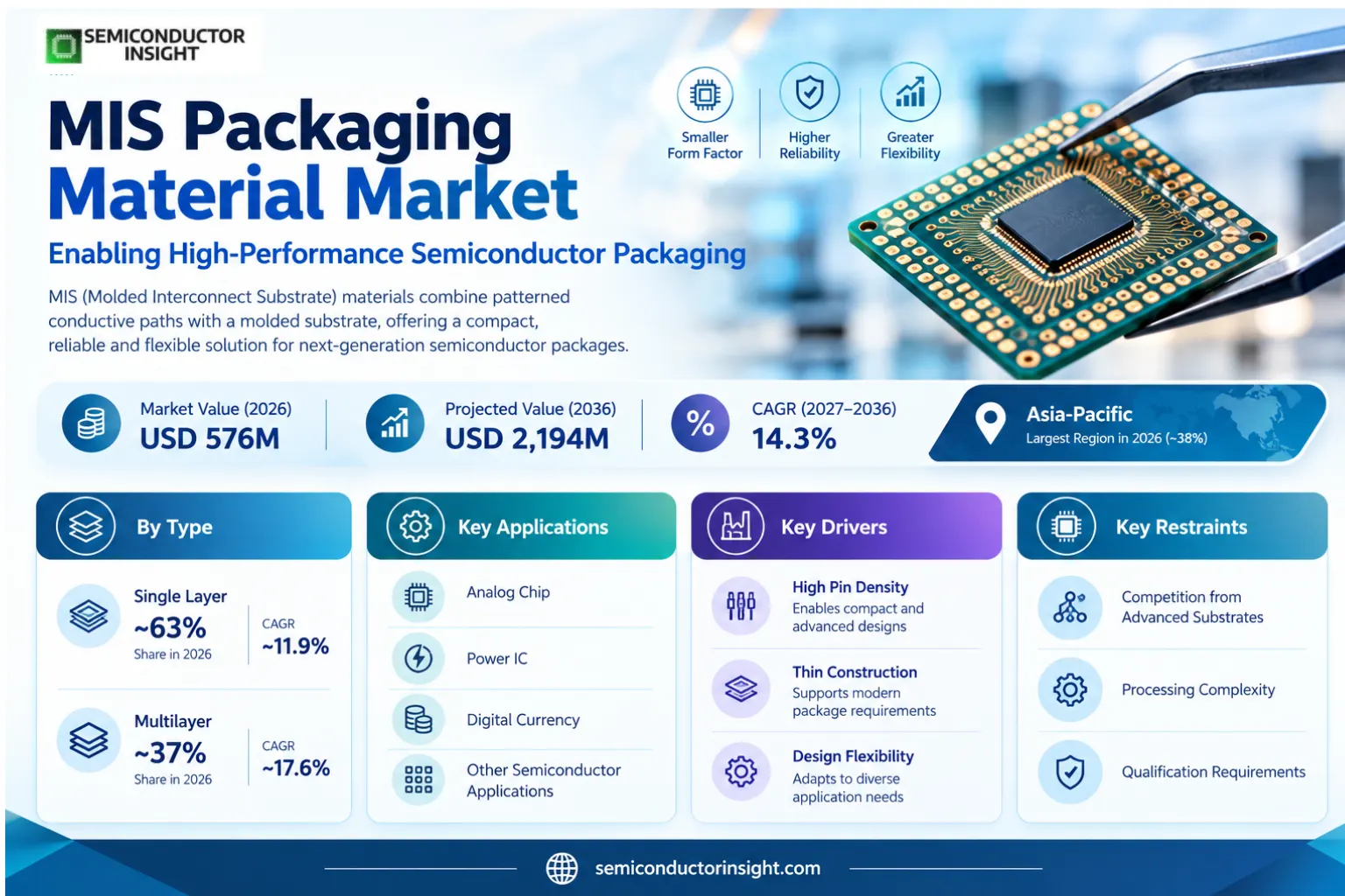
- Market value: the global MIS packaging material market reached USD 576 million in 2026 and is projected to reach USD 2,194 million by 2036, expanding at a CAGR of 14.3% over 2027–2036 as substrate routing density and low-profile semiconductor packaging gain importance.
- Single Layer substrates held the largest estimated 2026 type share at ~63%, reflecting lower interconnect complexity and suitability for mature analog and power-chip layouts; Multilayer substrates held ~37% and have the fastest modeled type growth of ~17.6% CAGR as routing density rises.
- Power IC packaging represented the largest application at an estimated ~40% of 2026 material value, ahead of Analog Chip at ~33%, Others at ~19% and Digital Currency at ~8%; demand is tied to package footprint, heat flow and qualification for low-profile designs.
- Asia-Pacific was the largest region with an estimated ~38% of 2026 revenue and the fastest modeled expansion at ~16.1% CAGR; QDOS documents substrate technology and manufacturing in Malaysia while QYC offers an MIS substrate category from Shenzhen.
- Supplier qualification is the decisive commercial restraint because fine-line yield, copper adhesion, molding compatibility and reliability screening must satisfy package assemblers before substrate material is adopted in analog, power and communication devices.
MIS Packaging Material Market Overview
The MIS packaging material market was valued at USD 576 million in 2026 and is projected to reach USD 2,194 million by 2036, growing at a CAGR of 14.3% over the 2027–2036 forecast period. Asia-Pacific was the largest regional market with an estimated ~38% share in 2026, reflecting semiconductor substrate fabrication and package-assembly networks in Malaysia and China.
Molded interconnect substrate, or MIS, is a packaging platform that combines patterned conductive paths with a molded structural substrate to route electrical signals between a semiconductor die and the external package contacts. It addresses the gap between a conventional stamped leadframe and a more elaborate organic package substrate. In this market the sold product is the interconnect substrate material supplied to packaging operations, not the assembled semiconductor device. Fine-pitch copper routing, thin construction and package design flexibility determine its commercial value.
The revenue boundary includes single-layer and multilayer MIS substrate materials sold for Analog Chip, Power IC, Digital Currency and other semiconductor applications. It excludes the semiconductor die, completed QFN or LGA package, assembly-and-test service, and general BT or ABF laminate products that are not supplied as MIS material. Unisem demonstrates how a finished MIS QFN package can incorporate the substrate: its product literature cites a profile as low as 0.33 mm, but that finished package is not itself the material revenue counted here.
Fabrication depends on copper patterning, substrate surface preparation, controlled dielectric and molding interfaces, and electrical inspection of increasingly fine interconnects. QDOS describes licensed MIS technology for flip-chip, wire-bonding and system-in-package designs at first-level interconnect and QFN, LGA and BGA configurations at the second level. Its semi-additive process capability and fine-line specifications show why material makers must coordinate closely with assembly customers: substrate geometry influences die placement, bond-wire clearance and package reliability.
Demand is concentrated where semiconductor packaging combines high pin density with severe limits on thickness and footprint. Analog components benefit from short routing paths and predictable parasitic behavior; power integrated circuits require attention to thermal resistance and current paths; communication devices favor compact layouts with reliable high-frequency performance. These applications do not automatically convert every finished package into MIS material demand. Revenue accrues only when a package design is actually qualified and supplied with an in-scope molded interconnect substrate.
Competition is shaped by two opposing trends. Packaging designers seek more routing density and thinner assemblies, creating an opening for MIS material, while advanced organic and wafer-level alternatives compete for the same engineering budgets. QDOS and QYC provide direct substrate evidence, whereas Unisem illustrates downstream use rather than independent material sales. The difference matters when interpreting manufacturing announcements or company financial statements: broad semiconductor packaging revenue cannot be equated with the narrowly defined MIS substrate-material market.
Segment Analysis: By Type
By Type, the market consists of Single Layer and Multilayer molded interconnect substrate material. Single Layer leads with an estimated ~63% of 2026 revenue and modeled ~11.9% CAGR, while Multilayer represents ~37% and is the fastest-growing type at ~17.6% CAGR. The split reflects different routing requirements and processing complexity rather than a claim about the share of all finished semiconductor packages.
| Type | Function | Market position |
|---|---|---|
| Single Layer | Single Layer MIS material uses one principal patterned routing plane to connect die pads and external terminals in compact leadless-package configurations. It is most appropriate when analog and power devices can meet signal integrity, current handling and thermal objectives without additional vertical interconnect complexity. Simpler conductor registration can improve process stability and lower inspection burden, but the technology becomes less attractive as pad counts and escape-routing requirements increase. | Largest type in 2026 (~63% share, ~11.9% CAGR). Its commercial advantage is compatibility with established leadframe-like package flows and simpler design verification. The estimated revenue lead does not imply that every QFN package uses MIS; conventional stamped leadframes remain important alternatives. Buyers typically compare fine-line capability, copper adhesion, moisture reliability and per-unit cost against the complexity of moving to a multilayer structure. |
| Multilayer | Multilayer MIS material provides more than one conductive routing level and associated interlayer connections, allowing tighter pad escape, more complex power or signal paths and potentially greater package integration. It requires additional alignment, dielectric, via and electrical-test controls. QYC describes broader package-substrate manufacturing from 2 to 26 layers, but those capabilities should not be interpreted as MIS-specific shipment volumes; they demonstrate the relevant manufacturing skill set. | Fastest-growing type (~37% share, ~17.6% CAGR). Adoption is most plausible where additional routing layers remove package-size constraints or replace a costlier interconnect solution. More processing steps create a yield penalty unless suppliers control trace definition and interlayer registration. Qualification can therefore be slower than for Single Layer products, while successful designs command higher material value per substrate and deepen the assembler relationship. |
Secondary commercial view: fine-pitch substrate configuration
Beyond the two published type classes, a useful commercial distinction separates fine-pitch leadframe-based MIS substrate configurations from other MIS layouts. Fine-pitch configurations account for an estimated ~58% of 2026 substrate-material value, compared with ~42% for other configurations. This is a separate analytical view of the same revenue base, not an additional product family to add to the Single Layer and Multilayer totals. It reflects QDOS fine-line processing and the use of copper routing in low-profile MIS QFN packages.
| Axis | Members | Commercial role |
|---|---|---|
| Substrate configuration | Fine-pitch leadframe-based substrates (~58%); Other MIS substrate configurations (~42%) | Fine-pitch leadframe-based designs concentrate the most demanding conductor-definition and molding-interface work, creating qualification advantages for substrate specialists. Other MIS configurations support customers with different pad pitches, package footprints and cost targets. Both categories sit within the same sold-material market, so their shares should be read as an alternative 100% allocation rather than additive revenue. |
Segment Analysis: By Application
By Application, Power IC material demand is largest at an estimated ~40% of 2026 revenue, followed by Analog Chip (~33%), Others (~19%) and Digital Currency (~8%). Power IC also has the fastest modeled application growth at ~16.3% CAGR, reflecting increased packaging complexity where thermal behavior and current routing must be balanced against low-profile footprints.
| Application | Demand characteristics |
|---|---|
| Analog Chip | Analog devices require controlled electrical paths between sensitive die nodes and external terminals, particularly when noise, parasitic capacitance and bond-wire geometry affect measurement accuracy. MIS substrate material offers compact copper routing and thin package geometry, although it must compete with established leadframe and laminate designs. The estimated ~33% application share in 2026 reflects a broad installed design base, with a modeled ~13.8% CAGR tied to gradual qualification of more complex analog packages. |
| Power IC | Power-management integrated circuits demand efficient current paths, predictable thermal performance and a package footprint that suits dense electronics assemblies. MIS material can support fine-pitch routing around multiple functional die, but designers must still assess resistance, copper thickness and thermal interfaces rather than assuming miniaturization alone improves performance. Power IC leads at an estimated ~40% of 2026 material value and has modeled ~16.3% CAGR as complex low-profile power designs expand. |
| Digital Currency | Digital-currency-related electronics can employ dense power-management and control packages, but their investment cycle is more volatile than automotive, industrial or general communications demand. The category is preserved because it is part of the published application scope, not because all computing hardware uses MIS material. Its estimated ~8% share and modeled ~9.9% CAGR reflect a smaller, cyclical opportunity where purchasing depends on specific device designs and customer qualification. |
| Others | Other applications include communications, consumer electronics, computing and automotive devices in which thin packages and additional copper routing can solve space constraints. Unisem explicitly identifies those end uses for its finished MIS package offering, demonstrating downstream technical relevance without establishing substrate sales by industry. This diverse group represents an estimated ~19% of 2026 material value and modeled ~12.0% CAGR, with design-specific rather than uniform adoption across customers. |
Application demand reaches substrate producers indirectly through package assemblers and semiconductor design teams. A die owner specifies electrical, mechanical and thermal requirements; an assembly partner chooses a viable package architecture; only then does a substrate supplier receive qualification and production orders. This sequence creates a longer sales cycle than selling commodity laminate. It also explains why technical documentation from a finished-package provider such as Unisem is useful evidence of application fit but not evidence of the substrate-material supplier’s revenue.
Regional Analysis
The MIS packaging material market is distributed across five regions: Asia-Pacific leads at an estimated ~38% of 2026 revenue, followed by North America (~31%), Europe (~20%), South America (~6%) and the Middle East & Africa (~5%). Asia-Pacific also has the highest modeled regional growth at ~16.1% CAGR, compared with ~12.3% in North America and ~14.2% in Europe. Regional allocations concern the material revenue chain, not the geographical location of every finished electronic device.
How does MIS substrate-material demand differ by region?
The geography of MIS substrate materials differs from that of semiconductor end consumption. QDOS documents a manufacturing base in Malaysia and describes MIS-related processing, while QYC lists an MIS substrate category in Shenzhen. North American and European semiconductor designers can influence material qualification without operating the substrate plant themselves. The resulting regional pattern reflects where packaging and substrate supply relationships generate revenue rather than a simple mapping of final electronic-device sales.
In 2023 the published North American MIS material value was USD 126.75 million against USD 386 million globally, or 32.8% of that year’s total. The estimated 2026 share is ~31%, allowing for different regional growth profiles rather than carrying forward the historical ratio. Europe is assigned ~20%, South America ~6% and the Middle East & Africa ~5%, with each regional figure an estimated allocation of the same global revenue base.
Technology and customer qualification create different market-access conditions. Asia-Pacific emphasizes proximity to substrate production and packaging assembly; North America emphasizes design wins and material traceability; Europe emphasizes industrial reliability and long product lifecycles. South America and the Middle East & Africa have smaller modeled shares because MIS material often arrives embedded within imported semiconductor packages, making the direct substrate transaction less visible in local downstream electronics statistics.
| Region | Position | Growth outlook | Demand profile | What decides supplier selection |
|---|---|---|---|---|
| Asia-Pacific | Largest (~38%) | Asia-Pacific has modeled ~16.1% CAGR, the fastest among the five regions. The principal commercial advantage is proximity between substrate processing and package assembly, as demonstrated by QDOS operations in Malaysia and QYC product availability in Shenzhen. Faster growth remains conditional on customer-specific yield and package qualification, rather than automatically following all regional semiconductor output. | Asian demand is linked to both direct substrate fabrication and the package assembly customers that qualify MIS materials. Malaysia offers a documented QDOS fine-line processing base, and China provides another advertised MIS substrate source through QYC. This concentration supports shorter engineering feedback loops, but broad integrated-circuit substrate capacity must not be counted entirely as molded interconnect material sales. | Customer selection in Asia-Pacific emphasizes copper trace definition, molded substrate consistency, process repeatability and the ability to coordinate with packaging lines. QDOS documents semi-additive processing while QYC advertises fine-line substrate capabilities. A qualified buyer still needs product-specific sample approval, defect screening and contractual continuity, because published manufacturing capabilities are not a substitute for evidence of production yield. |
| North America | Second largest (~31%) | North America has modeled ~12.3% CAGR, below the global rate, with a relatively strong historical revenue position. The published 2023 regional market was USD 126.75 million out of USD 386 million globally, providing a calibration point rather than a permanent share. Growth is tied to new package designs and material qualification decisions made by semiconductor customers that may outsource substrate fabrication. | The regional demand profile is shaped by semiconductor design and specification influence more than by a verified local MIS substrate manufacturing concentration. US designers can require compact analog, power and communications packages, while Canadian and Mexican electronics activity creates downstream exposure. Purchases of the in-scope material usually occur through international package supply chains after the exact substrate is approved. | North American customer approval commonly requires documented material origin, consistent conductor geometry, electrical performance and traceable quality controls. The commercial buyer may be a package assembler outside North America even when the die design originates there. MIS substrate vendors must distinguish a direct material supply agreement from a completed-package contract and demonstrate that the same approved process can be sustained over multiple lots. |
| Europe | Third largest (~20%) | Europe is modeled to expand at ~14.2% CAGR, with an estimated ~20% of global MIS material value in 2026. Demand is influenced by long-lived automotive and industrial semiconductor programmes, where a thin package must survive demanding service conditions. Qualification cycles can delay adoption, but successful material approval may support recurring orders over longer periods than short-cycle consumer electronics designs. | European packaging decisions emphasize reliability and technical documentation for power control, industrial sensing and communications devices. German automotive requirements can be particularly demanding, while France and the United Kingdom host specialty electronics design activity. The direct substrate may be manufactured elsewhere; the region contributes to MIS material value through specification and qualified sourcing rather than an assumed local factory count. | European customers scrutinize copper adhesion, dimensional stability, moisture exposure, thermal cycling and material change control before replacing an established package architecture. QDOS quality-system disclosures provide a relevant process-control example without proving a particular MIS medical-device qualification. Suppliers must show that the routing advantage justifies added inspection and that process revisions will not undermine reliability during long product lifecycles. |
| South America | Fourth (~6%) | South America has an estimated ~6% share of 2026 MIS material revenue and modeled ~13.2% CAGR. Its growth pathway is largely indirect: qualified MIS substrates enter the region embedded in imported semiconductors or devices. Consequently, the forecast should not be interpreted as a projection of locally produced MIS substrates, and currency or import-cost changes can influence the adoption of higher-value packages. | Brazil is a significant electronics end market, while Argentina, Chile and Colombia provide more selective industrial and communications demand. Local equipment producers typically purchase finished components, not raw MIS substrates, so material demand depends on package choices made earlier in the international value chain. Cost-sensitive programmes may continue using conventional leadframes when MIS routing does not deliver a compelling engineering benefit. | South American procurement focuses on the landed cost and continuity of approved packaged semiconductors, with less direct access to the underlying substrate vendor. The relevant MIS supplier opportunity comes from winning designs at international component makers serving the region. Technical traceability still matters for industrial applications, but a local distributor relationship should not be mistaken for direct substrate fabrication or independent MIS material revenue. |
| Middle East & Africa | Fifth (~5%) | The Middle East and Africa hold an estimated ~5% of 2026 global MIS material revenue, with modeled ~12.6% CAGR. The opportunity is associated with imported electronics for industrial, communications and infrastructure systems rather than verified large-scale local substrate production. Growth can arise as compact power and control packages are incorporated into equipment, but the material transaction generally occurs earlier in the global semiconductor chain. | The United Arab Emirates provides electronics distribution and systems-integration channels, Saudi Arabia has industrial and communications project demand, and South Africa has industrial-maintenance requirements. These activities can consume chips packaged with MIS materials, yet the substrate is rarely purchased directly by the end user. Regional demand must therefore be traced to approved component architectures rather than inferred from all electronics-project spending. | Market access depends on package qualification by the original semiconductor supplier, dependable international logistics and long-term component availability. An industrial buyer may care about service temperature and reliability without knowing which substrate technology is inside a chip. MIS material manufacturers benefit only where the upstream component design specifies their substrate, making direct supplier documentation and approved material revisions more important than regional marketing presence. |
Key MIS Packaging Material Manufacturers and Competitive Landscape
MIS substrate-material supply is a specialized part of semiconductor packaging, with fewer clearly documented direct material suppliers than the broader package-assembly industry. QDOS documents licensed MIS technology and substrate manufacturing, while QYC advertises MIS package substrates. The published company profile set includes MISpak, ASM, PPT, QDOS Technology and SIMMTECH, but inclusion in a profile does not establish that each company currently sells an exact-scope MIS substrate material.
QDOS has the clearest inspected direct technical evidence. It describes MIS technology used with flip-chip, wire-bonding and system-in-package first-level connections, as well as QFN, LGA and BGA package interfaces. Its semi-additive processing and fine-line capabilities address routing density and low-profile package requirements. A supplier with this combination of material processing and package-engineering support can compete through qualification and yield rather than relying only on the unit price of the substrate.
QYC lists MIS Package Substrate Manufacturer as a distinct category alongside BT, ABF, ceramic and other package substrates. The company describes wider manufacturing capabilities, including 2–26 layers and fine conductor geometry, but those broad specifications do not measure its MIS-only shipments. Its relevance is a potential qualified source for substrate designs, while its actual position depends on customer-specific MIS process evidence, production quality and commercial availability.
Unisem provides downstream evidence rather than direct independent material-supplier evidence. Its MIS QFN offering has a stated package thickness of 0.33 mm or lower and targets consumer, communications, data storage, computing and automotive uses. The finished-package specification helps establish why customers buy MIS substrates, but package assembly fees and completed-device revenue must be excluded from the material-market denominator. This separation prevents a broad assembly provider from being ranked as a material producer without supporting evidence.
ASMPT disclosed in its 26 February 2020 financial release that it had decided to discontinue its MIS business in the first quarter of 2020. ASM therefore remains in the published historical company profile set, but it is not classified as a current Tier 1 or Tier 2 MIS substrate-material supplier. MISpak, PPT and SIMMTECH likewise require product-specific verification before assigning present-day exact-scope supplier leadership; a general packaging or substrate catalogue alone is not a verified MIS material shipment.
Tier structure
| Tier | Companies | Basis of competition |
|---|---|---|
| Tier 1 | QDOS Technology | Direct evidence includes licensed MIS substrate technology, substrate fabrication, fine-line process capability and named package-interface applications. Qualification is based on the ability to translate a customer’s package drawing into reliable conductor patterns and molded substrate material, maintain electrical yield, and document repeatability across production lots. No numerical company market-share ranking is implied by this tier. |
| Tier 2 | Shenzhen QYC Technology | QYC explicitly advertises an MIS package-substrate category and broader advanced-substrate manufacturing capability. It represents a prospective alternative for customer-specific procurement where the requested MIS geometry and material specification can be qualified. The tier indicates documented product availability and potential competitive role, not verified MIS shipment volume or a claim that all of QYC’s 2–26-layer substrates are MIS products. |
| Downstream, former and unverified names | Unisem (finished-package assembler); ASMPT/ASM (former MIS business); MISpak; PPT; SIMMTECH | Unisem supplies finished MIS QFN package services, not a separately documented standalone MIS material product. ASMPT disclosed MIS discontinuation in 2020. MISpak, PPT and SIMMTECH are retained from the published competitive profile set but do not have sufficiently specific inspected current product evidence for ranking as direct MIS substrate-material producers. This distinction protects the revenue boundary and avoids converting adjacent company activity into market share. |
Key companies profiled
- MISpak
- ASM
- PPT
- QDOS Technology
- SIMMTECH
MIS Packaging Material Production Capacity Analysis
MIS material production is organized around fine-line substrate processing and customer-specific package qualification rather than an openly reported global nameplate-capacity series. QDOS identifies production and process capability in Malaysia and operations linked to China, while QYC lists an MIS substrate product family in Shenzhen. The important capacity variable is qualified, yield-adjusted output for a particular design, not the number of plants manufacturing all semiconductor substrates.
QDOS identifies a Batu Kawan facility established in 2018 and documents semi-additive processing relevant to molded interconnect substrates. Its product literature describes fine-line technology for several first- and second-level package interfaces. This demonstrates process capability, but no inspected official source separates MIS output from other QDOS printed-circuit and integrated-circuit substrate products. The commercial bottleneck is therefore qualifying the exact conductor geometry, materials and inspection recipe requested by each package customer.
QYC operates from Shenzhen and describes a wider substrate catalogue with fine conductor and multilayer capabilities. Those specifications show an engineering base from which an MIS design might be supplied, but they should not be treated as evidence of MIS production tonnage or annual material revenue. Customers need to verify tooling, layer registration, minimum trace specifications and sample yield for their own package. Capacity planning is consequently tied to approved product families rather than broad substrate-factory announcements.
Upstream constraints include copper surface preparation, dielectric and molding-material compatibility, plating chemistry, photoresist control, inspection equipment and substrate handling at thin gauges. More demanding multilayer designs can add process stages and scrap risk, so a nominally available factory line may not translate into immediately saleable MIS substrates. Suppliers with repeatable inspection and documented reliability performance can secure longer-running programmes, while failed qualification may leave capacity allocated to conventional substrate work.
MIS Packaging Material Market Dynamics: Drivers, Restraints and Opportunities
MIS material demand is supported by semiconductor package miniaturization, finer copper routing and the need to connect more functions within low-profile packages. Growth is constrained by customer qualification time, competing leadframe and laminate architectures, uncertain yield on demanding multilayer patterns and the difficulty of separating material value from finished-package revenue. The commercial opportunities are design-specific, particularly in power management, analog devices and compact communications electronics.
MARKET DRIVERS
Drivers Impact Analysis*
| Driver | (~) % impact on CAGR forecast | Geographic relevance | Impact timeline |
|---|---|---|---|
| Thin and fine-pitch semiconductor packaging | +2.1% | Asia-Pacific and North America | Medium term (2–4 years) |
| Power IC routing and compact device design | +1.8% | Global power and industrial electronics | Medium term (2–4 years) |
| More multilayer routing requirements | +1.6% | Asia-Pacific and Europe | Long term (4+ years) |
| Substrate supplier process improvements | +1.2% | Malaysia, China and qualified global buyers | Medium term (2–4 years) |
| Qualification of low-profile QFN applications | +0.8% | Global package assembly networks | Short term (up to 2 years) |
Low-profile packaging requires more routing options
The drive to reduce package height creates design pressure that cannot always be solved by a conventional stamped leadframe. Unisem documents a finished MIS package profile as low as 0.33 mm, showing the architecture’s potential. The relevant substrate-material demand appears when the die layout and terminal count require patterned copper traces that a simpler frame cannot provide, allowing an MIS supplier to win a qualified design rather than merely substitute a commodity material.
Power-management designs favor dense current paths
Power ICs are the largest modeled MIS application, at ~40% of 2026 material revenue. Power packages must balance footprint, conductor resistance, heat dissipation and mechanical robustness, so a more flexible routing substrate can be attractive when layout constraints dominate. This opportunity is not universal: high-current designs may still prefer conventional leadframes or other thermal structures, making the package-level cost and performance comparison central to customer adoption.
Multilayer routing expands the addressable designs
Multilayer MIS accounts for an estimated ~37% of 2026 value but has the fastest modeled type growth at ~17.6% CAGR. Additional routing planes can solve escape-routing and pad-density problems in more complex packages. However, each layer also raises registration and inspection requirements, so growth depends on demonstrated yield and the ability to justify the higher material value against organic substrates and other established alternatives.
Established Asian processing supports design iteration
QDOS describes semi-additive substrate processing and MIS-related product technology in Malaysia, while QYC advertises an MIS substrate category from Shenzhen. Proximity between fabrication engineers and packaging operations can shorten prototype iteration and defect investigation. Commercial orders still depend on package qualification, but access to fine-line processing and technical feedback creates a plausible route from a specialized substrate design to recurring production purchases.
MARKET RESTRAINTS
Restraints Impact Analysis*
| Restraint | (~) % impact on CAGR forecast | Geographic relevance | Impact timeline |
|---|---|---|---|
| Lengthy package qualification | −1.6% | North America, Europe and global OEM programmes | Long term (4+ years) |
| Competition from conventional leadframes | −1.3% | Global analog and commodity devices | Short term (up to 2 years) |
| Yield losses in fine-line multilayer processing | −1.1% | Asian substrate production | Medium term (2–4 years) |
| Mismatch between package and material revenues | −0.6% | Global supplier contracting | Medium term (2–4 years) |
Qualification delays postpone substrate orders
An MIS material supplier must prove copper adhesion, electrical continuity, moisture reliability and molding compatibility under the customer’s actual package process. A successful laboratory design may require additional lots and assembly trials before high-volume release. These steps protect device reliability but delay the point at which a technical win becomes recurring material revenue, especially in industrial and automotive programmes with long service expectations.
Standard leadframes remain cost-effective alternatives
Many analog and power devices can be packaged successfully with conventional leadframes that use established stamping, plating and assembly processes. MIS routing flexibility adds value only when a specific footprint, pad-count or electrical problem cannot be solved economically by the incumbent design. This substitution pressure is strongest for mature high-volume components, where even small changes in unit package cost influence supplier selection.
Fine-line process yield determines commercial economics
A substrate with dense copper traces requires reliable lithography, plating, surface preparation and inspection. QDOS and QYC describe fine-line capabilities, but capability statements are not evidence of guaranteed yield for every customer design. If defect rates rise as trace pitch narrows or layer count increases, effective production capacity and margins can deteriorate, delaying orders even when customer demand for compact packages is strong.
Broad packaging statistics can overstate MIS demand
Semiconductor assembly revenue includes die handling, bonding, encapsulation, testing and finished-package value that fall outside the MIS substrate-material boundary. Likewise, sales of ABF or BT substrates are not automatically MIS sales. Without this distinction, supplier growth announcements can appear to imply much larger MIS demand than the product-specific transactions justify, distorting procurement forecasts and investment decisions.
MARKET OPPORTUNITIES
Medical and regulated-device supply qualification
QDOS announced ISO 13485 quality-management recognition in June 2023, demonstrating attention to a regulated-device quality framework. The certification does not prove medical MIS shipments, but it can support conversations with buyers that demand traceable production records and controlled changes. Suppliers able to connect that quality discipline with a qualified thin-package substrate may enter programmes where reliability and documentation are more important than the lowest initial price.
Thin communications and computing packages
Unisem identifies communications, data storage and computing as uses for its MIS package offering. These applications can create opportunities for substrate suppliers when higher I/O density must fit a limited package outline. The winning material design needs to maintain electrical integrity and manufacturability, and suppliers should avoid assuming that every communications or computing package adopts MIS merely because the architecture is technically feasible.
Process integration and customer co-design
Fine-line semi-additive processing offers an opportunity for MIS suppliers to participate earlier in package design rather than receive fixed drawings after engineering decisions are complete. Collaboration can identify where conductor pitch, molding behavior and layer count influence cost and reliability. The commercial benefit is a higher probability of qualification and a more durable design position, though it also requires investment in engineering support and process documentation.
Regional supply resilience through qualified alternatives
QDOS and QYC provide two independently identifiable substrate-technology sources in Asia, while downstream assembly companies such as Unisem demonstrate the package demand pathway. Customers seeking supply resilience can qualify more than one compatible substrate process, but differences in conductor geometry, materials and inspection methods mean a second supplier cannot be assumed interchangeable without validation. Dual-source opportunities therefore reward disciplined process control and comparable test results.
MIS Packaging Material Supply Chain Analysis
The MIS substrate-material supply chain begins with copper, dielectric and molding-compatible process materials; proceeds through patterned substrate fabrication and inspection; and reaches semiconductor package assemblers that integrate the substrate with die, bonding and encapsulation. The finished package then moves through semiconductor component channels into electronics systems. Revenue counted here stops at the sold substrate material rather than following the entire value of the completed device.
Upstream. Copper quality, dielectric compatibility, surface treatment and plating chemistry influence conductor adhesion and fine-line definition. A small defect in a dense routing pattern can make a substrate unusable even when the bulk material meets specifications. Buyers therefore need traceable raw-material lots and control over chemistry changes. The same upstream materials may be used in adjacent substrate families, but those purchases are not all part of the MIS revenue base.
Manufacturing. Substrate producers pattern conductors, form any required interlayer connections, control dimensional stability and inspect electrical paths before shipping approved designs. QDOS documents semi-additive process capability and MIS technology; QYC describes broader fine-line substrate manufacturing. These disclosures establish technical pathways without proving specific MIS shipment volumes. Effective output depends on yield against a customer’s drawing, so qualification and inspection capability matter as much as equipment count.
Channel. Semiconductor package assemblers and die owners control the approved material list. A supplier may spend several design cycles matching conductor geometry, molding interfaces and electrical performance before a package is released for production. Unisem’s finished MIS QFN product illustrates the downstream integration point, but its assembly service revenue must not be added to the substrate-material market. Contracts are therefore won through design qualification and dependable repeatability.
Downstream. The material is embedded in analog, power, communications, computing and other semiconductor packages before it reaches equipment manufacturers. The downstream user generally purchases a completed chip, not a bare MIS substrate. As a result, end-market trends help identify where new package designs might emerge but cannot be used directly as MIS material sales. Package architecture and the qualified bill of materials determine the actual revenue conversion.
Recent Developments in the MIS Packaging Material Market
- 27 May 2026 Published
SEMI and Global Net Corp released an industry discussion of glass-core substrate development for semiconductors. Glass-core is an adjacent and potentially competing advanced-packaging pathway, not MIS material revenue. The significance for MIS suppliers is that customers are evaluating multiple interconnect architectures; substrate producers must demonstrate the specific cost, package-height and qualification advantages of molded interconnect designs rather than assume every advanced-packaging investment benefits MIS. Source - 10 February 2026 Reported
SEMI reported that worldwide silicon wafer shipments increased 5.8% during 2025 while wafer revenue declined 1.2%. The figures describe upstream wafers, not MIS substrate material, and show that unit activity and selling-price movements can diverge. MIS suppliers face a similar commercial distinction when estimating the value of qualified material shipments, particularly where product mix and process complexity change. Source - 22 June 2023 Announced
QDOS announced an ISO 13485 quality-management achievement. The certification is relevant to documentation, process control and traceability expectations in regulated electronics supply chains, although it does not establish that a particular MIS substrate design has medical-device approval. For substrate customers, a controlled quality system can support qualification discussions where material consistency and change management are central purchasing criteria. Source - 28 June 2021 Published
QDOS described its local manufacturing and engineering capabilities, including substrate operations associated with Penang and Xiamen and semi-additive processing. The company communication demonstrates a regional supply and technology base that can support MIS package-material development. It does not disclose a separate MIS revenue series, so the commercial relevance is production capability and engineering access rather than a quantified shipment increase. Source - 26 February 2020 Reported
ASMPT reported its 2019 results and stated that the MIS business would be discontinued in the first quarter of 2020. This is material to current competitive classification because ASM is included in historical MIS company lists but should not be described as an active direct supplier without contrary newer evidence. Buyers must distinguish former technology participants from currently qualified substrate-material manufacturers. Source - 2018 Announced
QDOS identifies 2018 as the establishment year of its Batu Kawan factory, within the company’s process-technology history. The milestone establishes a manufacturing-site chronology relevant to Malaysia’s fine-line substrate ecosystem, but the date alone does not prove the start of MIS mass production or quantify its capacity. Commercially, an established site provides a platform for subsequent customer-specific process qualification. Source
REPORT SCOPE & SEGMENTATION
| Attribute | Details |
|---|---|
| Study Period | 2021–2036 |
| Base Year | 2026 |
| Estimated Year | 2027 |
| Forecast Period | 2027–2036 |
| Historical Period | 2021–2025 |
| Market Size 2026 | USD 576 million |
| Market Size 2027 | USD 659 million |
| Market Size 2036 | USD 2,194 million |
| Growth Rate | CAGR of 14.3% from 2027–2036 |
| Unit | Value (USD Million) of sold MIS substrate packaging material |
| Segmentation | By Type, By Application, By Substrate Configuration and By Region |
| By Type | Single Layer · Multilayer |
| By Application | Analog Chip · Power IC · Digital Currency · Others |
| By Substrate Configuration | Fine-pitch leadframe-based substrates · Other MIS substrate configurations |
| By Region | Regions evaluated by Type, Application, substrate configuration and Country North AmericaUnited States, Canada, Mexico EuropeGermany, France, United Kingdom, Rest of Europe Asia-PacificChina, Japan, South Korea, Malaysia, Southeast Asia, India, Rest of Asia-Pacific South AmericaBrazil, Argentina, Chile, Colombia, Rest of South America Middle East & AfricaSaudi Arabia, United Arab Emirates, South Africa, Rest of Middle East & Africa |
| Key Companies Profiled | MISpak, ASM, PPT, QDOS Technology, SIMMTECH |
| Customization Scope | Country and package-architecture scope may be customized, including fine-line conductor specifications, supplier qualification criteria, and distinctions between standalone MIS material and completed semiconductor packages. |
Frequently Asked Questions
What is the size of the global MIS packaging material market?
The global MIS packaging material market was valued at USD 576 million in 2026 and is projected to reach USD 2,194 million by 2036, representing a CAGR of 14.3% over the 2027–2036 forecast period. Demand arises from qualified low-profile semiconductor packages that use patterned molded interconnect substrate material rather than conventional leadframes or other interconnect architectures.
What does MIS packaging material include?
MIS packaging material consists of molded interconnect substrates with patterned conductive routing sold to semiconductor packaging operations. It includes single-layer and multilayer substrate material used in qualifying analog, power and other devices. The revenue boundary excludes the semiconductor die, completed QFN package, assembly and testing services, and other substrate technologies when they are not sold as MIS material.
Which companies supply MIS packaging material?
QDOS documents licensed MIS technology and substrate manufacturing, and QYC advertises an MIS package-substrate product category. Unisem offers finished MIS QFN packages, which is a downstream role rather than independent material supply. ASMPT disclosed that its MIS business was discontinued in the first quarter of 2020. Other historically profiled names require direct product verification before supplier ranking.
Which MIS substrate type is largest?
Single Layer MIS substrate material held an estimated ~63% of 2026 revenue and has modeled ~11.9% CAGR because simpler routing structures suit many compact analog and power packages. Multilayer material represented ~37% and has faster modeled ~17.6% CAGR where additional routing planes solve higher pad density or escape-routing problems. Both shares apply to the same MIS material market.
What are the major applications for MIS material?
Power IC packaging is the largest modeled application at ~40% of 2026 revenue, followed by Analog Chip at ~33%, Others at ~19% and Digital Currency at ~8%. These categories reflect package-material use rather than semiconductor end-product revenue. Adoption depends on whether MIS copper routing improves the required electrical, thermal and mechanical performance at an acceptable qualified package cost.
Which region leads MIS packaging material demand?
Asia-Pacific leads with an estimated ~38% of 2026 MIS substrate-material revenue and modeled ~16.1% CAGR. QDOS documents MIS technology and manufacturing capability in Malaysia, while QYC advertises an MIS substrate category in Shenzhen. North America follows at ~31%, Europe at ~20%, South America at ~6% and the Middle East & Africa at ~5%.
Why is MIS material used in thin semiconductor packages?
MIS material allows patterned copper interconnects within a compact molded substrate structure, potentially reducing package footprint while accommodating more routing complexity than a conventional stamped leadframe. Unisem describes a finished MIS QFN package profile of 0.33 mm or lower, demonstrating architectural feasibility. Actual benefits depend on the chip layout, current paths, electrical noise, thermal performance and qualification results.
What limits adoption of MIS substrates?
The principal barriers are qualification time, fine-line manufacturing yield, molding-interface reliability and competition from lower-cost conventional leadframes or alternative organic substrates. A substrate maker must prove copper adhesion, dimensional consistency and electrical continuity for a customer-specific package. Broader semiconductor packaging investment does not automatically generate MIS material revenue because only approved designs produce recurring substrate orders.
How does multilayer MIS differ from single-layer MIS?
Multilayer MIS uses additional conductor routing levels and interlayer connections to manage higher pad density or complex signal and power paths. It can support designs that exceed the routing capability of a single layer, but increases alignment, inspection and processing demands. Its modeled ~17.6% CAGR exceeds the single-layer ~11.9% rate because more demanding designs can justify added material value.
What years and segments does the study cover?
The study uses 2026 as the base year, 2027 as the estimated year and 2027–2036 as the forecast period, with historical context for 2021–2025. It covers Single Layer and Multilayer types; Analog Chip, Power IC, Digital Currency and Others applications; fine-pitch versus other MIS substrate configurations; and five world regions. Values measure sold substrate material rather than completed packages.
Research Sources & Evidence Base
Get Sample Report PDF for Exclusive Insights
Report Sample Includes
- Table of Contents
- List of Tables & Figures
- Charts, Research Methodology, and more...
 Download Sample Report PDF