MARKET INSIGHTS
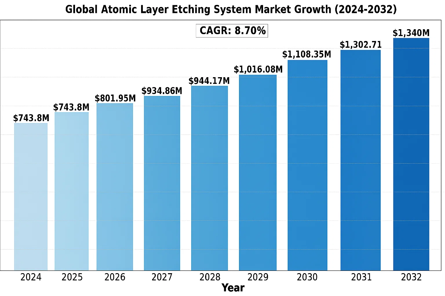
The Global Atomic Layer Etching System Market size was valued at US$ 743.8 million in 2024 and is projected to reach US$ 1.34 billion by 2032, at a CAGR of 8.7% during the forecast period 2025-2032.
Atomic Layer Etching (ALE) systems are precision semiconductor manufacturing tools that enable atomic-scale material removal through sequential self-limiting surface reactions. These systems utilize plasma-based or thermal processes to achieve ultra-precise etching capabilities for advanced semiconductor fabrication. The technology is critical for manufacturing next-generation logic and memory chips with 3D architectures at sub-7nm nodes.
The market growth is driven by increasing demand for miniaturized semiconductor devices, transition to EUV lithography processes, and rising investments in advanced packaging technologies. While the plasma-type ALE systems currently dominate the market, high-temperature variants are gaining traction for specialized applications. Key industry players like Lam Research and Applied Materials are actively expanding their ALE portfolios through R&D investments, with recent breakthroughs in selective etching capabilities for 3D NAND and DRAM manufacturing.
MARKET DYNAMICS
MARKET DRIVERS
Increasing Demand for Advanced Semiconductor Devices to Fuel ALE Adoption
The global semiconductor industry’s relentless pursuit of miniaturization and performance enhancement is driving significant demand for atomic layer etching systems. As transistor sizes shrink below 5nm nodes, traditional plasma etching techniques face limitations in precision and selectivity. Atomic layer etching addresses these challenges by enabling exacting control at the atomic scale, with etch depth accuracy better than 0.1nm per cycle. This precision is becoming crucial for manufacturing cutting-edge logic and memory devices, where even single-atom variations can impact performance. Recent data shows that the market for advanced semiconductor devices requiring such precision etching is growing at over 12% annually.
Expansion of 3D NAND and DRAM Manufacturing to Boost Market Growth
The transition to 3D NAND flash memory and advanced DRAM architectures presents a major growth opportunity for ALE systems. Unlike planar NAND, 3D NAND requires precise etching of deep, high-aspect ratio structures with extreme uniformity across the wafer. Atomic layer etching has proven essential for maintaining structural integrity in these complex 3D architectures, particularly as layer counts exceed 200 in next-generation devices. Leading memory manufacturers are increasingly adopting ALE technology, with production volumes for 3D NAND projected to grow by over 18% in the next three years. This rapid expansion directly correlates to increased demand for advanced etching systems capable of handling these challenging requirements.
Government Support for Semiconductor Self-Sufficiency to Accelerate Investments
Global initiatives aimed at strengthening domestic semiconductor capabilities are creating a favorable environment for ALE system adoption. Government programs like the CHIPS Act in the United States and similar initiatives in Europe and Asia are allocating substantial funding for advanced semiconductor manufacturing equipment. This includes dedicated support for next-generation technologies like atomic layer etching that enable continued scaling and innovation. Recent reports indicate that semiconductor equipment investments in leading manufacturing regions could exceed $120 billion annually by 2025, with a significant portion directed toward advanced process technologies requiring ALE capabilities.
MARKET RESTRAINTS
High Initial Investment and Operational Costs to Limit Market Penetration
Despite its technological advantages, atomic layer etching systems face significant adoption barriers due to their high capital and operational costs. A complete ALE toolset can require investments exceeding $10 million per system, with additional expenses for specialized facilities, gases, and maintenance. While these costs are justified for leading-edge nodes below 7nm, they present financial challenges for manufacturers operating older technology nodes or with limited R&D budgets. This cost sensitivity is particularly evident in emerging semiconductor regions where investment capital is constrained, potentially slowing broader market adoption of ALE technology.
Technical Complexity and Process Development Challenges to Hamper Growth
The implementation of atomic layer etching presents substantial technical hurdles that could restrain market expansion. ALE processes require precise synchronization of multiple parameters including gas flow rates, plasma conditions, and temperature control to maintain atomic-level accuracy. This complexity extends development cycles and increases the need for specialized process expertise. Many chip manufacturers report that integrating ALE into existing production lines can require 12-18 months of process development and qualification, creating a significant barrier to rapid adoption. Furthermore, the need for continuous process optimization as node sizes decrease adds ongoing technical challenges that require substantial R&D investment.
Material Selectivity and Throughput Limitations to Impact Adoption
While atomic layer etching offers unmatched precision, current implementations face limitations in material selectivity and throughput that could slow market growth. Most ALE systems demonstrate excellent selectivity between materials like silicon and silicon oxide, but struggle with more complex material combinations used in advanced devices. Additionally, the cyclic nature of ALE processes results in significantly lower throughput compared to conventional plasma etching methods. Recent studies indicate that ALE throughput typically ranges between 1-10nm per minute, which poses productivity challenges for high-volume manufacturing despite the superior precision advantages.
MARKET CHALLENGES
Supply Chain Vulnerabilities to Test Market Resilience
The atomic layer etching system market faces mounting challenges from global supply chain instability. Critical components like precision plasma sources, vacuum systems, and specialized chamber materials often depend on limited suppliers, creating potential bottlenecks. Recent events have shown that disruptions in the semiconductor equipment supply chain can delay deliveries by six months or more. This situation is exacerbated by the complex nature of ALE systems, which incorporate numerous high-specification components from specialized manufacturers. Ensuring stable, diversified supply chains while maintaining rigorous quality standards presents an ongoing challenge for equipment providers and semiconductor manufacturers alike.
Other Challenges
Technological Convergence Requirements
The integration of atomic layer etching with other advanced patterning techniques like EUV lithography creates complex tool-matching challenges. Synchronizing ALE processes with the tighter overlay and critical dimension requirements of EUV-patterned wafers demands extensive co-optimization efforts.
Workforce Development Gaps
The industry faces a growing shortage of engineers skilled in both ALE technology and advanced semiconductor processes. Training programs struggle to keep pace with the rapid evolution of etching technologies, creating talent bottlenecks that could delay adoption timelines.
MARKET OPPORTUNITIES
Emerging Applications in Advanced Packaging to Open New Growth Avenues
Beyond traditional front-end semiconductor manufacturing, atomic layer etching is finding growing applications in advanced packaging technologies. The rise of heterogeneous integration and 3D packaging schemes creates demand for precision etching in through-silicon vias (TSVs), micro-bumps, and interconnects. ALE’s ability to achieve highly uniform etching across diverse materials makes it particularly valuable for these emerging packaging applications. Industry analysts project that the advanced packaging equipment market will grow at nearly 15% annually, presenting significant opportunities for ALE system suppliers to expand beyond their core foundry and memory customers.
Development of Novel Materials Systems to Expand Addressable Market
The semiconductor industry’s exploration of new channel materials beyond silicon creates additional opportunities for atomic layer etching technology. Materials like gallium nitride (GaN), silicon carbide (SiC), and various 2D materials require precise etching techniques that conventional methods struggle to deliver. ALE’s material-specific, self-limiting reactions make it uniquely suited for these emerging material systems. Recent breakthroughs in III-V compound semiconductor etching demonstrate ALE’s potential to become the preferred solution for next-generation power electronics and RF devices, potentially opening multi-billion dollar market segments in the coming years.
Collaborative R&D Initiatives to Accelerate Technology Adoption
Strategic partnerships between equipment manufacturers, semiconductor companies, and research institutions are creating significant opportunities for ALE technology advancement. Several industry consortia have launched dedicated programs to address key challenges in atomic-scale processing, focusing on improving throughput, selectivity, and process control. These collaborative efforts are expected to yield new ALE architectures and chemistries that could dramatically expand the technology’s applicability and cost-effectiveness. Recent announcements suggest that major semiconductor manufacturers are increasing their ALE-related R&D budgets by over 20% annually to capitalize on these collaborative opportunities.
GLOBAL ATOMIC LAYER ETCHING SYSTEM MARKET TRENDS
Emerging Demand for Precise Semiconductor Fabrication Technologies
The global atomic layer etching (ALE) system market is experiencing accelerated growth due to rising demand for ultra-precise semiconductor manufacturing at nanometer scales. With the semiconductor industry’s progression beyond 5nm nodes, ALE has become critical for achieving atomic-level precision in etching without damaging underlying structures. Industry projections suggest the ALE market could grow at a compound annual growth rate of approximately 22% through 2030, driven by its indispensable role in next-generation logic and memory chips. Recent innovations including directional plasma ALE have further expanded capabilities for 3D NAND and gate-all-around transistor architectures.
Other Trends
Adoption in Advanced Packaging Technologies
The rapid expansion of heterogenous integration and advanced packaging solutions has created new opportunities for ALE systems. Fan-out wafer-level packaging (FOWLP) and 3D IC stacking increasingly require ALE’s selective material removal capabilities at interfacial layers. Leading foundries are investing heavily in this technology, with estimated capacity expansions exceeding 30% year-over-year for advanced packaging applications. This aligns with broader industry shifts toward chiplet-based designs that push the limits of conventional etching techniques.
Increasing R&D Investments in Atomic Precision Manufacturing
Global semiconductor R&D expenditures surpassed $150 billion annually, with a significant portion directed toward process technologies enabling atomic-scale control. National initiatives like the U.S. CHIPS Act and Europe’s Chips Act have catalyzed additional investments in next-generation fabrication tools, including ALE systems. Collaborations between academic institutions and equipment manufacturers are yielding notable breakthroughs in thermal ALE processes for novel materials. Furthermore, the integration of machine learning for process optimization is creating new efficiency benchmarks, achieving up to 40% improvement in etch uniformity compared to conventional methods.
COMPETITIVE LANDSCAPE
Key Industry Players
Semiconductor Equipment Leaders Drive Innovation in Precision Etching Solutions
The global atomic layer etching (ALE) system market features a moderately concentrated competitive environment, dominated by established semiconductor equipment manufacturers and emerging technology specialists. Lam Research currently leads the market with approximately 28% revenue share in 2023, owing to its pioneering work in plasma-based ALE solutions and strong partnerships with major foundries.
Applied Materials and Tokyo Electron Limited (TEL) collectively account for nearly 40% of the market, benefiting from their comprehensive etch product portfolios and longstanding relationships with memory and logic chip manufacturers. These companies continue to invest heavily in R&D, with Lam alone allocating over $1.6 billion annually to etching technology development.
The competitive intensity is increasing as mid-sized players like Hitachi High-Tech and Oxford Instruments expand their ALE offerings, particularly for emerging applications in 3D NAND and advanced packaging. These challengers are gaining traction through specialized solutions that address specific process challenges in next-generation semiconductor manufacturing.
List of Key Atomic Layer Etching System Manufacturers
- Lam Research Corporation (U.S.)
- Applied Materials, Inc. (U.S.)
- Tokyo Electron Limited (Japan)
- Hitachi High-Tech Corporation (Japan)
- Oxford Instruments plc (UK)
- Corial (France)
- NAURA Technology Group Co., Ltd. (China)
- Veeco Instruments Inc. (U.S.)
- ASM International NV (Netherlands)
Segment Analysis:
By Type
Plasma Type Segment Leads Due to Superior Precision in Semiconductor Manufacturing
The market is segmented based on type into:
- Plasma Type
- High Temperature Type
- Others
By Application
Transistor Segment Dominates Owing to Rising Demand for Advanced Electronics
The market is segmented based on application into:
- Transistor
- Extreme Ultraviolet Lithography
- Others
By End User
Semiconductor Foundries Account for Largest Share Due to High-volume Production Needs
The market is segmented based on end user into:
- Semiconductor Foundries
- Integrated Device Manufacturers
- Research Institutions
Regional Analysis: Global Atomic Layer Etching System Market
North America
The North American atomic layer etching (ALE) system market is characterized by significant technological innovation and strong semiconductor industry presence. Leading companies like Lam Research and Applied Materials dominate the landscape, driven by consistent R&D investments in advanced semiconductor manufacturing. The U.S. CHIPS Act, which allocated $52.7 billion for domestic semiconductor research and production, is accelerating demand for precision etching technologies. While the plasma-type ALE segment leads in adoption for transistor applications, high-temperature variants are gaining traction in extreme ultraviolet (EUV) lithography processes. Stringent process control requirements in advanced nodes (5nm and below) are pushing manufacturers to adopt atomic-level precision solutions.
Europe
European demand for ALE systems shows steady growth, with particular strength in specialized research applications. Oxford Instruments and other regional players are advancing plasma-based etching solutions that align with EU sustainability directives. The market benefits from collaborative semiconductor initiatives like the European Chips Act, which aims to double the EU’s global semiconductor market share to 20% by 2030. However, compared to Asia and North America, adoption in volume production remains limited. Academic and research institutions represent a significant customer segment, utilizing ALE for novel material development and quantum computing applications. The market faces challenges from the region’s comparatively smaller semiconductor manufacturing base.
Asia-Pacific
Asia-Pacific represents the fastest-growing and largest ALE system market globally, accounting for over 60% of worldwide semiconductor production capacity. China’s push for semiconductor self-sufficiency, demonstrated through initiatives like the “Big Fund” with $50 billion allocated, is driving unprecedented equipment investments. Not only do established manufacturers (TEL, Hitachi High-Tech) maintain strong positions, but domestic players like NAURA are gaining share in the mid-range segment. While transistor manufacturing accounts for majority demand, the rapid adoption of EUV lithography in Korea and Taiwan is creating new opportunities. However, price sensitivity in emerging markets and geopolitical trade tensions present ongoing challenges for equipment suppliers.
South America
The South American ALE market remains in nascent stages, with limited local semiconductor manufacturing infrastructure. Most demand stems from academic research institutions and specialized industrial applications rather than high-volume production. Brazil shows the most activity, with select universities and government research centers adopting ALE systems for advanced materials studies. Economic volatility and reliance on imported equipment constrain market expansion. However, growing interest in developing local tech capabilities, particularly in Brazil and Argentina, suggests potential long-term opportunities. Currently, market development is hampered by limited access to the latest generation systems and dependence on foreign suppliers for maintenance and support.
Middle East & Africa
MEA represents a developing market with several strategic initiatives showing promise. The United Arab Emirates and Saudi Arabia are making targeted investments in semiconductor-related technologies as part of broader economic diversification plans. While current ALE adoption is minimal, planned projects like the $100 million semiconductor design initiative in Abu Dhabi could stimulate future demand. South Africa maintains some research activities at academic institutions, focusing on specialized applications rather than commercial production. The region faces significant challenges including lack of established semiconductor ecosystem and dependence on foreign expertise, though government-backed technology parks and special economic zones may foster gradual market development over the next decade.
Report Scope
This market research report provides a comprehensive analysis of the Global and regional Atomic Layer Etching System markets, covering the forecast period 2025–2032. It offers detailed insights into market dynamics, technological advancements, competitive landscape, and key trends shaping the industry.
Key focus areas of the report include:
- Market Size & Forecast: Historical data and future projections for revenue, unit shipments, and market value across major regions and segments.
- Segmentation Analysis: Detailed breakdown by product type, technology, application, and end-user industry to identify high-growth segments and investment opportunities.
- Regional Outlook: Insights into market performance across North America, Europe, Asia-Pacific, Latin America, and the Middle East & Africa, including country-level analysis where relevant.
- Competitive Landscape: Profiles of leading market participants, including their product offerings, R&D focus, manufacturing capacity, pricing strategies, and recent developments such as mergers, acquisitions, and partnerships.
- Technology Trends & Innovation: Assessment of emerging technologies, integration of AI/IoT, semiconductor design trends, fabrication techniques, and evolving industry standards.
- Market Drivers & Restraints: Evaluation of factors driving market growth along with challenges, supply chain constraints, regulatory issues, and market-entry barriers.
- Stakeholder Analysis: Insights for component suppliers, OEMs, system integrators, investors, and policymakers regarding the evolving ecosystem and strategic opportunities.
Primary and secondary research methods are employed, including interviews with industry experts, data from verified sources, and real-time market intelligence to ensure the accuracy and reliability of the insights presented.
FREQUENTLY ASKED QUESTIONS:
What is the current market size of Global Atomic Layer Etching System Market?
-> The global Atomic Layer Etching System market size was valued at US$ 743.8 million in 2024 and is projected to reach US$ 1.34 billion by 2032, at a CAGR of 8.7% during the forecast period 2025-2032.
Which key companies operate in Global Atomic Layer Etching System Market?
-> Key players include Lam Research, Applied Materials, TEL, Hitachi High-Tech, Oxford Instruments, Corial, and NAURA Technology, among others.
What are the key growth drivers?
-> Key growth drivers include increasing demand for advanced semiconductor devices, miniaturization of ICs, and adoption of EUV lithography in chip manufacturing.
Which region dominates the market?
-> Asia-Pacific dominates the market with over 60% share, driven by semiconductor manufacturing hubs in Taiwan, South Korea, and China.
What are the emerging trends?
-> Emerging trends include integration of AI in etching processes, development of atomic-scale manufacturing, and adoption of ALE for 3D NAND and DRAM production.

Get Sample Report PDF for Exclusive Insights
Report Sample Includes
- Table of Contents
- List of Tables & Figures
- Charts, Research Methodology, and more...