MARKET INSIGHTS
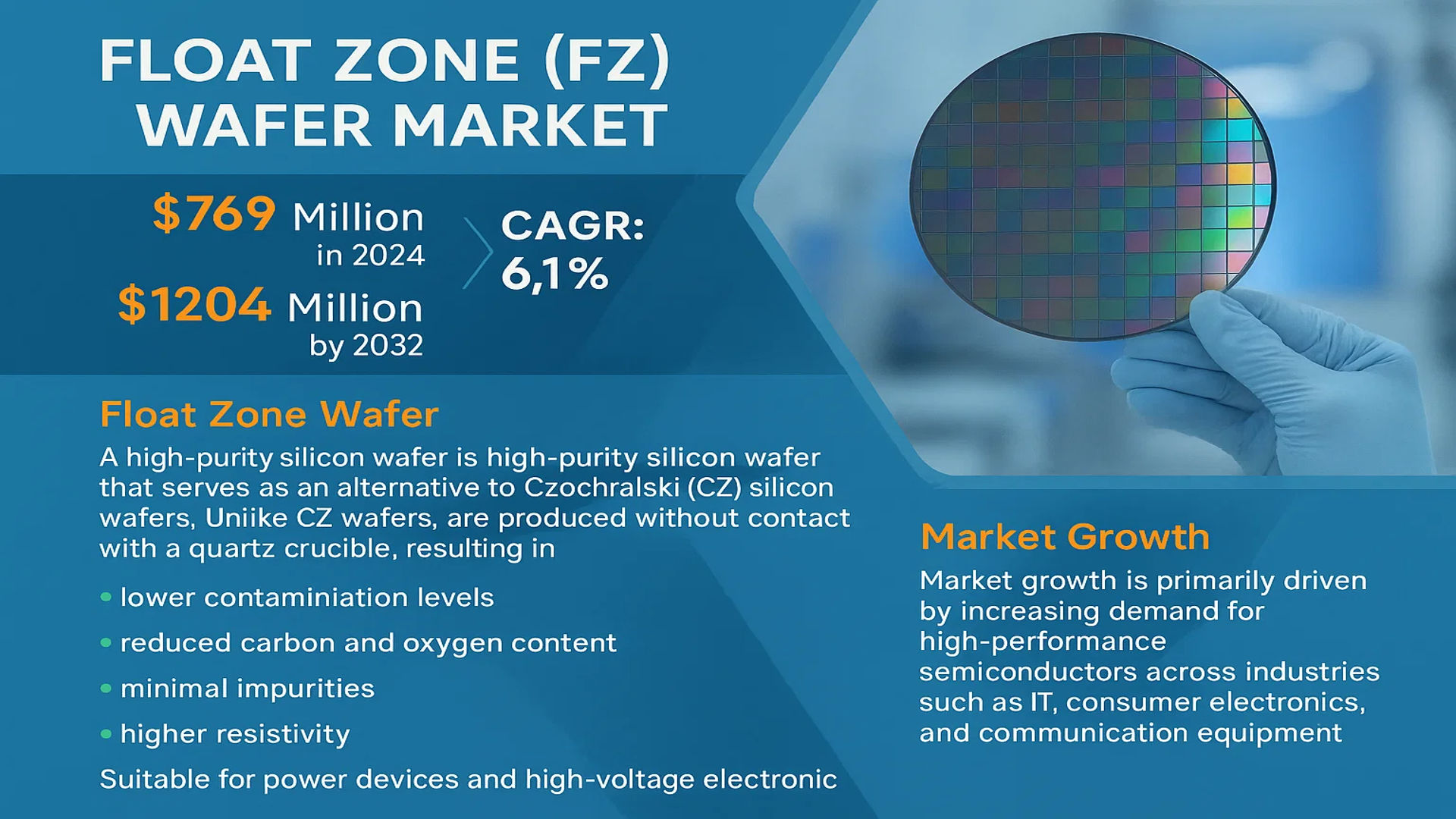
The global Float Zone (FZ) Wafer market was valued at 769 million in 2024 and is projected to reach US$ 1204 million by 2032, at a CAGR of 6.1% during the forecast period.
Float Zone Wafer is a high-purity silicon wafer that serves as an alternative to conventional Czochralski (CZ) silicon wafers. Unlike CZ wafers, FZ wafers are produced without contact with a quartz crucible, resulting in significantly lower contamination levels. This production method yields wafers with reduced carbon and oxygen content, minimal impurities, and higher resistivity, making them ideal for power devices and high-voltage electronic applications.
The market growth is primarily driven by increasing demand for high-performance semiconductors across industries such as IT, consumer electronics, and communication equipment. Furthermore, emerging applications in quantum computing and optical communication are creating new opportunities, as FZ wafers meet the stringent purity requirements of these advanced technologies. Key players like Shin-Etsu Chemical, SUMCO, and Siltronic are investing in production innovations to enhance efficiency and reduce costs, further accelerating market expansion.
MARKET DYNAMICS
MARKET DRIVERS
Increased Demand for High-Power Semiconductors to Drive Growth
The global Float Zone (FZ) Wafer market is experiencing significant growth, primarily driven by the surging demand for high-power semiconductor devices. These wafers, known for their superior purity and low defect density, are becoming increasingly critical in power electronics applications. Industries such as automotive, renewable energy, and industrial automation are rapidly adopting FZ wafers for manufacturing insulated-gate bipolar transistors (IGBTs) and power MOSFETs. The market for power semiconductors is projected to exceed $50 billion by 2030, creating substantial opportunities for FZ wafer suppliers.
Quantum Computing Advancements Accelerate Adoption
Quantum computing development represents another major growth driver for the FZ wafer market. The extreme purity requirements of quantum bit fabrication make FZ wafers the material of choice for emerging quantum technologies. Major tech companies and research institutions are investing heavily in quantum computing, with global funding exceeding $30 billion in recent years. This technological frontier demands silicon substrates with exceptionally low oxygen content and minimal crystal defects – specifications that standard Czochralski-grown wafers cannot meet.
Additionally, the integration of FZ wafers in photonic devices for optical communication networks provides another growth avenue. The expansion of 5G infrastructure and data centers worldwide is creating sustained demand for high-quality optical components manufactured using FZ silicon.
MARKET RESTRAINTS
High Production Costs Limit Market Penetration
While FZ wafers offer superior performance characteristics, their significantly higher production costs compared to conventional wafers remain a key market restraint. The float zone process requires specialized equipment and consumes more energy than standard crystal growth methods. Production yields are typically lower due to the technical challenges of maintaining optimal process conditions. These factors result in FZ wafer prices being more than double those of comparable CZ wafers.
Technical Limitations in Larger Diameter Production
The FZ process faces physical constraints when producing larger diameter wafers, limiting adoption in some mainstream semiconductor applications. While CZ wafer production has successfully transitioned to 300mm and larger diameters, FZ wafer manufacturing predominantly remains at 200mm and below. This size limitation restricts use in certain high-volume manufacturing processes optimized for larger wafer sizes.
Moreover, the stringent control required during the float zone process makes scaling production capacity challenging. Manufacturers must maintain exacting standards for temperature gradients, rotation speeds, and atmosphere control throughout the crystal growth process.
MARKET OPPORTUNITIES
Emerging High-Frequency Applications Present New Growth Areas
The expansion of 5G and future 6G networks creates significant opportunities for FZ wafer suppliers. These advanced communication technologies require components capable of operating at extremely high frequencies with minimal signal loss. FZ wafers’ low impurity levels and high resistivity make them ideal for manufacturing RF devices and millimeter-wave integrated circuits used in next-generation base stations and satellite communications.
Automotive Electrification Drives Demand for Power Devices
The global shift toward electric vehicles presents another major opportunity for the FZ wafer market. Modern EVs require sophisticated power management systems incorporating high-voltage silicon carbide and gallium nitride devices. While these wide-bandgap semiconductors often use alternative substrates, the development of hybrid solutions combining SiC with FZ silicon is gaining traction. As EV production volumes continue to rise, the demand for advanced power electronics will create a parallel need for high-quality FZ wafers.
Furthermore, government initiatives supporting semiconductor independence in key regions are leading to increased investments in specialized wafer production facilities. Various national programs are allocating substantial funding to develop domestic capabilities in advanced semiconductor materials, including FZ silicon.
MARKET CHALLENGES
Supply Chain Vulnerabilities Impact Production Stability
The FZ wafer market faces significant supply chain challenges, particularly regarding the availability of ultra-high purity polysilicon feedstock. The production of FZ-grade polysilicon requires even more stringent purity standards than standard semiconductor-grade material. With only a handful of suppliers capable of meeting these requirements, any disruption can have immediate impacts on wafer production capacity.
Technological Competition from Alternative Materials
Emerging substrate technologies present competitive challenges to FZ silicon wafers. Silicon-on-insulator (SOI) wafers and gallium arsenide substrates are gaining ground in certain RF and power applications. While FZ wafers maintain advantages in specific high-performance applications, ongoing improvements in alternative materials continue to pressure the market position of traditional FZ silicon.
Additionally, the development of advanced epitaxial growth techniques allows conventional CZ wafers to approach some performance characteristics of FZ wafers at lower costs. Manufacturers must continually innovate to maintain their technological edge in this competitive landscape.
FLOAT ZONE (FZ) WAFER MARKET TRENDS
Rising Demand for High-Purity Semiconductors Drives FZ Wafer Market Growth
The Float Zone (FZ) Wafer market is witnessing robust growth due to increasing demand for high-purity silicon substrates in advanced semiconductor applications. With oxygen content below 1 ppma and resistivity exceeding 1,000 ohm-cm, FZ wafers offer superior performance for power devices and quantum computing applications. This segment accounted for nearly 32% of high-end wafer production last year, reflecting its critical role in next-generation electronics. The automotive industry’s transition to electric vehicles has particularly accelerated adoption, where FZ wafers enable more efficient IGBT modules for power conversion.
Other Trends
Quantum Computing Breakthroughs
Major technology firms are investing heavily in quantum research infrastructure, creating unprecedented demand for ultra-pure silicon substrates. FZ wafers have demonstrated 10x lower defect density compared to conventional CZ wafers in qubit fabrication trials, making them the material of choice for superconducting quantum processors. Recent developments in cryogenic electronics further amplify this trend, with testing showing significantly improved coherence times when using FZ-based architectures.
Optoelectronics Industry Expansion
The photonics sector is driving innovation in FZ wafer applications, particularly for integrated optical circuits and LiDAR systems. With refractive index uniformity below 0.0001 across 300mm wafers, FZ silicon enables precise light manipulation in emerging photonic devices. Telecom companies are adopting these wafers for next-generation optical modulators that demonstrate 40% lower insertion losses compared to traditional materials. This aligns with global 5G infrastructure deployments requiring higher frequency operation and better signal integrity.
Manufacturing Process Advancements
Recent innovations in zone refining techniques have increased FZ wafer yield rates from 65% to nearly 82% for 200mm diameter production. Automated crystal diameter control systems now maintain tolerances within ±0.5mm during growth, while advanced dopant uniformity technologies achieve resistivity variations below 5% across the wafer surface. These improvements address historical production challenges that previously limited market penetration, with new manufacturing facilities reporting 30% reduction in per-wafer energy consumption through optimized heating systems.
COMPETITIVE LANDSCAPE
Key Industry Players
Semiconductor Giants and Emerging Players Drive Innovation in High-Purity Wafer Solutions
The global Float Zone (FZ) Wafer market features a dynamic competitive landscape with strong participation from both established semiconductor material suppliers and specialized manufacturers. While the market remains partially consolidated, with the top five players accounting for approximately 58% of global revenue in 2024, innovation from mid-sized companies continues to reshape the industry dynamics. Leading wafer producers like Shin-Etsu Chemical and SUMCO dominate through their vertical integration capabilities and extensive R&D investments in crystal growth technologies.
Recent market analysis shows Asian manufacturers gaining significant traction, with companies like Zhonghuan Advanced and GlobalWafers expanding their FZ wafer production capacities by 20-25% annually since 2022. This strategic expansion directly addresses the growing demand from power electronics and optical communication sectors. Meanwhile, European players such as Siltronic maintain technological leadership in ultra-high resistivity wafers, particularly for quantum computing applications where material purity is critical.
The competitive intensity is further amplified by technological partnerships across the value chain. GRINM Semiconductor Materials recently entered into collaboration with three major IGBT manufacturers to develop application-specific wafer solutions, demonstrating how customization is becoming a key differentiator. At the same time, smaller specialized firms like WaferPro are capturing niche segments through innovative thinning and polishing techniques that reduce post-processing costs.
Investment trends reveal that over 35% of industry R&D expenditure in 2023-24 focused on defect reduction and diameter scaling, with several companies transitioning from 6-inch to 8-inch wafer production. Market leaders are simultaneously pursuing strategic acquisitions to strengthen their intellectual property portfolios – a notable example being GlobalWafers’ 2023 acquisition of a German specialty wafer manufacturer to enhance its FZ technology pipeline.
List of Key Float Zone (FZ) Wafer Companies Profiled
- Shin-Etsu Chemical Co., Ltd. (Japan)
- SUMCO Corporation (Japan)
- Siltronic AG (Germany)
- GlobalWafers Co., Ltd. (Taiwan)
- Zhonghuan Advanced Semiconductor Materials (China)
- Beijing Jingyuntong Technology Co., Ltd. (China)
- Luoyang Hongtai Semiconductor Co., Ltd. (China)
- GRINM Semiconductor Materials (China)
- WaferPro LLC (U.S.)
- PlutoSemi Technologies (U.S.)
Segment Analysis:
By Type
8-Inch Float Zone Wafers Dominate the Market Due to Widespread Adoption in Power Electronics
The market is segmented based on wafer size into:
- Less than 6-inch
- 8-inch
By Application
Power Devices Segment Leads Market Growth with Increasing Demand for High-Voltage Components
The market is segmented based on application into:
- MEMS (Micro-Electro-Mechanical Systems)
- Transistors
- IGBT (Insulated Gate Bipolar Transistors)
- RF Devices
- Optical Communication Equipment
- Others
By End User
Semiconductor Manufacturers Drive Demand for High-Purity Float Zone Wafers
The market is segmented based on end users into:
- Semiconductor Foundries
- IDMs (Integrated Device Manufacturers)
- Research Institutions
- Defense & Aerospace Organizations
By Material Characteristics
High Resistivity Wafers Gain Traction in RF and Power Applications
The market is segmented based on material properties into:
- Standard Resistivity Wafers
- High Resistivity Wafers
- Ultra-High Purity Wafers
Regional Analysis: Float Zone (FZ) Wafer Market
Asia-Pacific
The Asia-Pacific region dominates the Float Zone (FZ) Wafer market, accounting for the largest revenue share in 2024. China and Japan are key contributors, driven by their robust semiconductor manufacturing ecosystems and heavy investments in advanced electronics. China’s “Made in China 2025” initiative has accelerated demand for high-purity silicon wafers, particularly in power devices and optical communication applications. Meanwhile, Japan benefits from technological leadership in precision manufacturing, with companies like Shin-Etsu Chemical and SUMCO maintaining strong FZ wafer production capabilities. The region’s expanding electric vehicle and renewable energy sectors further propel demand for IGBTs and power modules that rely on FZ silicon.
North America
North America maintains a strong position in the FZ wafer market, particularly in high-end applications like quantum computing and RF devices. The U.S. leads with significant R&D investments from both government agencies (e.g., Department of Energy initiatives) and private tech giants developing next-gen semiconductors. Silicon Valley’s focus on AI hardware and 5G infrastructure drives demand for ultra-high-resistivity FZ wafers. However, reliance on Asian suppliers for volume production creates supply chain vulnerabilities, prompting reshoring efforts under the CHIPS Act. Canada shows growing activity in quantum technologies utilizing FZ silicon substrates.
Europe
Europe’s FZ wafer market thrives on specialized industrial and automotive applications, particularly in Germany and France. Stringent quality standards make FZ wafers essential for premium automotive power electronics and industrial IGBT modules. The region benefits from strong collaborations between research institutes like Fraunhofer and wafer manufacturers to develop advanced materials for photonics applications. However, higher production costs compared to Asia challenge market expansion. Recent EU initiatives like the Chips Act aim to bolster local semiconductor capabilities, potentially benefiting FZ wafer producers serving niche high-performance segments.
South America
South America represents an emerging market for FZ wafers, with Brazil showing gradual adoption in power electronics for renewable energy systems. Limited local manufacturing capabilities mean most wafers are imported primarily from Asia and North America. Economic volatility and underdeveloped semiconductor infrastructure constrain market growth, though increasing investments in solar energy and electric mobility present long-term opportunities. The lack of specialized foundries capable of processing high-purity FZ wafers remains a key barrier to broader market penetration across the region.
Middle East & Africa
The MEA region shows nascent demand for FZ wafers, concentrated in Israel’s growing tech sector and Saudi Arabia’s diversification into advanced electronics. Israel’s strong semiconductor design industry creates some demand for specialty wafers, though local fab capabilities remain limited. Most countries rely entirely on imports due to absent domestic silicon processing facilities. While the market currently represents a small fraction of global demand, planned technology hubs like Saudi Arabia’s NEOM could stimulate future growth in high-end semiconductor materials as regional digital transformation accelerates.
Report Scope
This market research report provides a comprehensive analysis of the global Float Zone (FZ) Wafer market, covering the forecast period 2025–2032. It offers detailed insights into market dynamics, technological advancements, competitive landscape, and key trends shaping the industry.
Key focus areas of the report include:
- Market Size & Forecast: Historical data and future projections for revenue, unit shipments, and market value across major regions and segments. The Global Float Zone (FZ) Wafer market was valued at USD 769 million in 2024 and is projected to reach USD 1204 million by 2032, growing at a CAGR of 6.1%.
- Segmentation Analysis: Detailed breakdown by product type (Less than 6 inch, 8 inch), application (MEMS, Transistor, IGBT, RF Device, Optical Communication), and end-user industry to identify high-growth segments and investment opportunities.
- Regional Outlook: Insights into market performance across North America, Europe, Asia-Pacific, Latin America, and the Middle East & Africa, including country-level analysis. Asia-Pacific dominates the market with over 60% share in 2024.
- Competitive Landscape: Profiles of leading market participants including Shin-Etsu Chemical, Siltronic, SUMCO, GlobalWafers, and Zhonghuan Advanced, covering their product portfolios, manufacturing capacities, and strategic initiatives.
- Technology Trends & Innovation: Assessment of emerging semiconductor fabrication techniques, including advancements in quantum computing materials, optoelectronic applications, and low-defect control technologies.
- Market Drivers & Restraints: Evaluation of factors such as growing demand for high-performance power devices versus challenges like high production costs and technical complexities.
- Stakeholder Analysis: Strategic insights for semiconductor manufacturers, equipment suppliers, investors, and policymakers regarding the evolving market ecosystem.
The research methodology combines primary interviews with industry experts and comprehensive analysis of verified market data to ensure accuracy and reliability.
FREQUENTLY ASKED QUESTIONS:
What is the current market size of Global Float Zone (FZ) Wafer Market?
-> Float Zone (FZ) Wafer market was valued at 769 million in 2024 and is projected to reach US$ 1204 million by 2032, at a CAGR of 6.1% during the forecast period.
Which key companies operate in Global Float Zone (FZ) Wafer Market?
-> Key players include Shin-Etsu Chemical, Siltronic, SUMCO, GlobalWafers, Zhonghuan Advanced, and Beijing Jingyuntong Technology, among others.
What are the key growth drivers?
-> Key growth drivers include rising demand for power electronics, quantum computing applications, and advancements in optical communication technologies.
Which region dominates the market?
-> Asia-Pacific dominates the market with over 60% share, driven by semiconductor manufacturing in China, Japan, and South Korea.
What are the emerging trends?
-> Emerging trends include adoption in quantum computing, development of larger wafer sizes (8-inch), and integration with advanced power devices.

Get Sample Report PDF for Exclusive Insights
Report Sample Includes
- Table of Contents
- List of Tables & Figures
- Charts, Research Methodology, and more...