Key Statistics
Key Takeaways
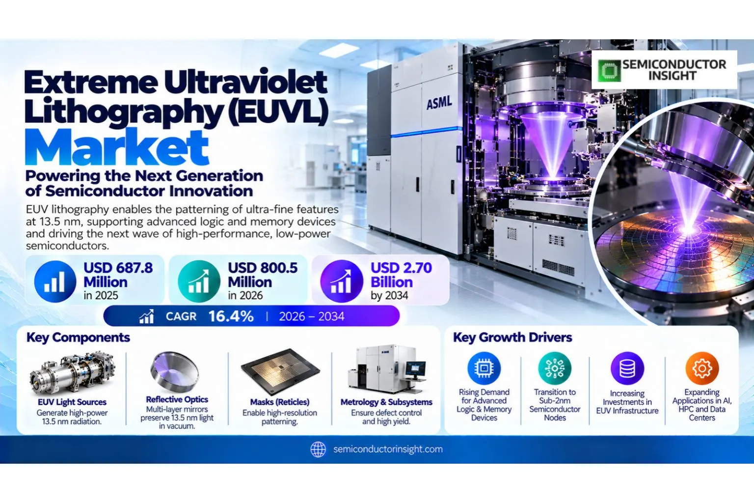
- The market is valued at USD 687.8 million in 2025 and is projected to reach USD 2.70 billion by 2034, representing a 16.4% CAGR over 2026–2034.
- Light Source is a major product segment, while adjacent variants are expanding as performance, integration and cost requirements evolve.
- Foundry is a leading application area, supported by demand across Integrated Device Manufacturers.
- Asia Pacific is the largest market in 2025 based on current demand, manufacturing concentration and ecosystem maturity.
Extreme Ultraviolet Lithography (EUVL) Market Overview
Extreme Ultraviolet Lithography (EUVL) uses 13.5 nm light and reflective optics to pattern the smallest critical layers in advanced semiconductor manufacturing. Unlike deep-ultraviolet systems, EUV operates in vacuum and relies on multilayer mirrors because conventional lenses absorb the wavelength. The resulting tool is among the most complex production systems in modern semiconductor fabs.
The market is entering a second technology phase as 0.55 NA High-NA systems move from qualification into production use. High-NA increases imaging contrast and resolution, allowing selected layers to be printed with less multipatterning. Commercial growth therefore depends not only on scanner shipments but also on masks, resists, metrology, source power and installed-base upgrades.
Segment Analysis: By Type
EUV light sources and reflective optics carry the highest technical value because the system must generate and preserve 13.5 nm radiation through multiple mirrors in vacuum. Masks, metrology and supporting subsystems remain strategically important because defects or reflectivity losses directly reduce patterning yield. Within this segment, customers increasingly compare lifecycle support, qualification requirements, integration effort and total ownership cost rather than relying on a single specification or upfront price.
| Type | Market relevance |
|---|---|
| Light Source | Laser-produced plasma and source subsystems. |
| Mirrors | Multilayer reflective optics and projection mirrors. |
| Mask | Reflective reticles and mask infrastructure. |
| Others | Metrology, stages, vacuum and supporting modules. |
Segment Analysis: By Application
Foundries and IDMs are the two principal customer groups because only advanced logic and memory manufacturers can economically deploy EUV at scale. Foundries emphasize broad node roadmaps and utilization, while IDMs optimize EUV insertion around proprietary logic or DRAM process flows. Within this segment, customers increasingly compare lifecycle support, qualification requirements, integration effort and total ownership cost rather than relying on a single specification or upfront price.
| Application | Market relevance |
|---|---|
| Foundry | Largest multi-customer leading-edge deployment base. |
| Integrated Device Manufacturers | Captive logic and memory manufacturing. |
Segment Analysis: By Technology Generation
0.33 NA NXE systems remain the production workhorse for advanced logic and memory, while 0.55 NA High-NA EXE systems expand single-exposure resolution and reduce selected multipatterning steps. Adoption depends on throughput, overlay, mask strategy and total wafer cost. Within this segment, customers increasingly compare lifecycle support, qualification requirements, integration effort and total ownership cost rather than relying on a single specification or upfront price.
| Technology Generation | Market relevance |
|---|---|
| 0.33 NA EUV | 13 nm resolution production platform. |
| 0.55 NA High-NA EUV | 8 nm resolution next-generation platform. |
Segment Analysis: By Process Role
Logic patterning currently represents the broadest leading-edge use, while DRAM EUV intensity is increasing as memory scaling advances. EUV mask, resist and metrology infrastructure expands alongside scanner deployment because defect control and process monitoring become more demanding at tighter dimensions. Within this segment, customers increasingly compare lifecycle support, qualification requirements, integration effort and total ownership cost rather than relying on a single specification or upfront price.
| Process Role | Market relevance |
|---|---|
| Logic Patterning | Advanced-node logic critical layers. |
| DRAM Patterning | Leading-edge DRAM scaling. |
| EUV Mask & Metrology | Mask inspection, resist and pattern-control ecosystem. |
Regional Analysis
Asia Pacific is the largest demand region because Taiwan, South Korea and Japan contain leading foundry and memory manufacturing, while Europe supplies critical lithography technology and North America is accelerating High-NA adoption through Intel and advanced-fab investment. Regional share also reflects supplier depth, engineering support, manufacturing concentration and the speed at which new Extreme Ultraviolet Lithography (EUVL) designs can move from evaluation into repeat deployment.
| Region | 2025 Position | Growth Outlook | Demand Profile |
|---|---|---|---|
| Asia Pacific | Largest | Very strong | Foundry and memory manufacturing led |
| North America | High-NA adoption hub | Very strong | Leading-edge logic and R&D led |
| Europe | Technology supply hub | Strong | Lithography equipment and optics led |
| South America | Emerging | Selective | Research and downstream electronics led |
| Middle East & Africa | Early-stage | Selective | Technology investment and research led |
Detailed Regional Blocks
Why is Asia Pacific important to this market?
Asia Pacific leads because TSMC, Samsung and other advanced manufacturers operate large EUV fleets for logic and memory. Regional demand spans scanners, masks, resists, inspection and installed-base service, making lithography intensity a major capital-spending driver. In Asia Pacific, procurement decisions also depend on service coverage, qualification resources, logistics and long-term availability, so ecosystem maturity can materially influence adoption even when core technology performance is similar.
| Country / Subregion | Role | Market Context |
|---|---|---|
| Taiwan | Leading foundry demand | TSMC uses EUV across advanced logic nodes. |
| South Korea | Logic and memory hub | Samsung expands EUV into logic and future DRAM. |
| Japan | Materials and mask ecosystem | Photoresist, mask and metrology suppliers support EUV production. |
- ASML’s 2026 roadmap positions NXE systems for 2 nm logic and leading-edge DRAM while High-NA EXE systems support sub-2 nm logic and future memory.
- Samsung and ASML announced in September 2026 that Samsung plans High-NA EUV adoption for future DRAM manufacturing.
- Mask, resist and metrology demand rises with every additional EUV layer because process-control requirements tighten as feature dimensions shrink.
Why is North America important to this market?
North America is strategically important because Intel has been the first customer to move High-NA EUV into selected high-volume manufacturing layers. U.S. fab expansion also creates demand for new scanners, service and process-control infrastructure. In North America, procurement decisions also depend on service coverage, qualification resources, logistics and long-term availability, so ecosystem maturity can materially influence adoption even when core technology performance is similar.
| Country / Subregion | Role | Market Context |
|---|---|---|
| United States | High-NA production leader | Intel and advanced fabs drive adoption. |
| Canada | Research and design niche | Direct scanner demand remains limited. |
- ASML reported in July 2026 that Intel was using High-NA EUV on selected Intel 18A production layers.
- ASML and Intel stated in September 2026 that more than one million wafers had been processed across certification, R&D and selected production use on High-NA systems.
- High-value EUV service and upgrade demand expands as the installed base grows.
Why is Europe important to this market?
Europe is the technology center because ASML in the Netherlands and ZEISS in Germany provide the scanner and projection-optics platform underpinning global EUV production. Regional value capture is therefore heavily weighted toward equipment and precision subsystems rather than wafer consumption. In Europe, procurement decisions also depend on service coverage, qualification resources, logistics and long-term availability, so ecosystem maturity can materially influence adoption even when core technology performance is similar.
| Country / Subregion | Role | Market Context |
|---|---|---|
| Netherlands | Global scanner hub | ASML is the sole commercial supplier of EUV scanners. |
| Germany | Optics and laser ecosystem | ZEISS and TRUMPF provide critical EUV subsystems. |
| Belgium | R&D ecosystem | imec supports advanced-node lithography development. |
- ASML’s EXE:5200B uses 0.55 NA optics and is designed for 8 nm resolution.
- The system provides 40% more imaging contrast than NXE platforms and supports single-exposure features 1.7 times smaller.
- European supplier concentration makes optics, source and precision-mechatronics capacity strategically important.
Why is South America important to this market?
South America is a very small direct EUV market because no leading-edge high-volume EUV fabs operate in the region. Demand is primarily indirect through imported advanced semiconductors and research collaborations. In South America, procurement decisions also depend on service coverage, qualification resources, logistics and long-term availability, so ecosystem maturity can materially influence adoption even when core technology performance is similar.
| Country / Subregion | Role | Market Context |
|---|---|---|
| Brazil | Largest regional research base | Academic and semiconductor programs create limited indirect demand. |
| Argentina | Research niche | No commercial EUV fab base. |
- EUV capital intensity prevents deployment outside leading semiconductor clusters.
- Most regional value consumption arrives embedded in advanced imported chips.
- Research participation is more realistic than direct scanner ownership.
Why is Middle East & Africa important to this market?
Middle East and Africa remain early-stage for direct EUV deployment. Israel has advanced semiconductor manufacturing and R&D, while Gulf technology investment could support longer-term advanced-fab ambitions. In Middle East & Africa, procurement decisions also depend on service coverage, qualification resources, logistics and long-term availability, so ecosystem maturity can materially influence adoption even when core technology performance is similar.
| Country / Subregion | Role | Market Context |
|---|---|---|
| Israel | Advanced semiconductor base | Existing fabs and design centers create adjacent demand. |
| United Arab Emirates | Technology-investment niche | Long-term semiconductor ambitions may create future opportunity. |
| Saudi Arabia | Emerging semiconductor strategy | Direct EUV demand remains prospective. |
- EUV adoption requires a complete leading-edge fab ecosystem, not only a scanner purchase.
- Supplier service infrastructure and mask capability are prerequisites for sustainable operation.
- Near-term demand is mainly indirect through advanced imported devices.
Competitive Landscape
ASML dominates commercial EUV scanner systems, while ZEISS, TRUMPF, KLA, Lasertec, TOPPAN, HOYA, AGC and other suppliers provide optics, sources, masks, inspection and supporting technologies. Competitive advantage is defined by nanometer-scale imaging, source power, throughput, overlay, uptime and process-control integration.
| Company | Position | Relevant capability |
|---|---|---|
| ASML | Key participant | Sole commercial EUV scanner supplier with NXE and High-NA EXE platforms. |
| Carl Zeiss SMT | Key participant | Critical projection and illumination optics partner for EUV and High-NA systems. |
| TRUMPF | Key participant | Competes through product breadth, integration capability, qualification and customer support. |
| KLA Corporation | Key participant | Mask, wafer and process-control systems supporting EUV production. |
| Lasertec | Key participant | Competes through product breadth, integration capability, qualification and customer support. |
| TOPPAN | Key participant | Competes through product breadth, integration capability, qualification and customer support. |
| HOYA Corporation | Key participant | Competes through product breadth, integration capability, qualification and customer support. |
| AGC | Key participant | Competes through product breadth, integration capability, qualification and customer support. |
| Applied Materials | Key participant | Competes through product breadth, integration capability, qualification and customer support. |
| Tokyo Electron | Key participant | Competes through product breadth, integration capability, qualification and customer support. |
Production Capacity Analysis
EUV capacity is constrained by precision optics, source systems, mechatronics and highly specialized assembly rather than conventional semiconductor wafer production. Scanner output is measured in tens of systems per year, so each incremental tool materially affects global advanced-node capacity. Scaling output without degrading consistency requires stable upstream materials, disciplined process control and final testing that catches performance drift before products reach high-value customer systems.
ASML stated in Q2 2026 that its low-NA EUV capacity was around 65 systems for 2026 and that it planned to add 30% more capacity for 2027, with further expansion under evaluation for 2028. Installed-base upgrades also increase effective wafer throughput. Second-source planning and regional technical support therefore become increasingly important as deployments expand and buyers seek supply continuity without repeating lengthy qualification work.
Market Dynamics
The market is driven by lithography intensity as much as wafer capacity. Each migration to a smaller logic or DRAM node can add EUV layers or shift layers from multipatterned DUV into single-exposure EUV, increasing equipment and service demand per fab. This is changing competitive behavior because vendors increasingly sell system-level value, workflow integration and lifecycle economics rather than an isolated component specification.
High-NA introduces a new adoption curve. Customers must balance higher resolution against tool cost, throughput, stitching and mask strategy, so production insertion will be selective by layer rather than an immediate full replacement of 0.33 NA EUV. Buyers consequently evaluate total ownership cost, qualification effort and roadmap stability across the life of a program instead of focusing only on initial purchase price.
Market Drivers
| Factor | Analyst Interpretation |
|---|---|
| Advanced-node scaling | 2 nm and below logic requires tighter patterning and reduced multipatterning complexity. |
| DRAM EUV intensity | Memory scaling is increasing the number of EUV-enabled critical layers. |
| AI chip demand | Advanced accelerators drive leading-edge logic and HBM-related fab investment. |
| High-NA readiness | Production qualification creates a new equipment generation and upgrade cycle. |
Market Restraints
| Factor | Analyst Interpretation |
|---|---|
| Extreme capital cost | EUV scanners and supporting fab infrastructure require very large investment. |
| Supply concentration | ASML is the sole commercial scanner supplier and key subsystems are highly concentrated. |
| Mask and resist complexity | Defect control and materials performance become harder at tighter dimensions. |
| Throughput economics | High-NA must deliver sufficient wafers per hour to justify layer insertion. |
Market Opportunities
| Factor | Analyst Interpretation |
|---|---|
| High-NA production ramp | Sub-2 nm logic and future DRAM create a new scanner generation. |
| Installed-base productivity upgrades | Higher source power and platform upgrades can expand effective capacity. |
| EUV mask innovation | Larger-format masks and improved inspection can raise future productivity. |
| Metrology and inspection | Tighter features increase demand for defect review and critical-dimension control. |
Supply Chain Analysis
The EUV value chain integrates light-source technology, ultra-precision mirrors, vacuum systems, masks, photoresists, stages, metrology and scanner assembly. Each subsystem operates near fundamental physical limits, making supplier qualification unusually stringent. Traceability and coordination between component suppliers, integrators and end users are important because failures found late in the chain can be far more expensive than the underlying part itself.
| Supply Chain Stage | Role in the Market |
|---|---|
| EUV source and laser subsystems | High-power laser-produced plasma generates 13.5 nm light. |
| Reflective optics and masks | Multilayer mirrors and reticles guide and pattern EUV radiation. |
| Scanner integration | Stages, vacuum, optics and control systems are assembled into NXE or EXE tools. |
| Fab process ecosystem | Resist, mask inspection, metrology and service enable high-volume production. |
Recent Developments
| Date | Development | Source |
|---|---|---|
| September 2026 | Intel Foundry and ASML reported continued High-NA production use, with more than one million wafers processed across certification, R&D and selected volume manufacturing. | ASML |
| September 2026 | TSMC and ASML announced an initiative targeting a 12-inch High-NA EUV photomask pilot line by 2031 to improve future productivity and reduce stitching constraints. | ASML |
| July 2026 | ASML announced the first High-NA EUV use on selected high-volume Intel 18A product layers. | ASML |
Report Scope & Segmentation
| Scope Item | Coverage |
|---|---|
| Base Year | 2025 |
| Estimated Year | 2026 |
| Forecast Period | 2026–2034 |
| 2025 Market Size | USD 687.8 million |
| 2026 Estimated Size | USD 800.5 million |
| 2034 Forecast Size | USD 2.70 billion |
| CAGR (2026–2034) | 16.4% |
| Largest Market in 2025 | Asia Pacific |
| Category | Semiconductor Equipment / Lithography / EUV |
| By Type | Light Source, Mirrors, Mask, Others |
| By Application | Foundry, Integrated Device Manufacturers |
| By Technology Generation | 0.33 NA EUV, 0.55 NA High-NA EUV |
| By Process Role | Logic Patterning, DRAM Patterning, EUV Mask & Metrology |
Frequently Asked Questions
What is the 2025 market size of the Extreme Ultraviolet Lithography (EUVL) market?
The market is valued at USD 687.8 million in 2025.
What is the projected 2034 market size of the Extreme Ultraviolet Lithography (EUVL) market?
The market is projected to reach USD 2.70 billion by 2034.
What is the CAGR of the Extreme Ultraviolet Lithography (EUVL) market from 2026 to 2034?
The market is expected to expand at a CAGR of 16.4% during 2026–2034.
Which region leads the Extreme Ultraviolet Lithography (EUVL) market?
Asia Pacific is the largest market in 2025 based on the current demand, manufacturing and deployment structure.
Which type segment is important in the Extreme Ultraviolet Lithography (EUVL) market?
Light Source is a major segment, while adjacent product variants are gaining share as performance and integration requirements evolve.
What is the main application for Extreme Ultraviolet Lithography (EUVL) products?
Foundry is a leading application, with additional growth coming from Integrated Device Manufacturers.
What drives growth in the Extreme Ultraviolet Lithography (EUVL) market?
2 nm and below logic requires tighter patterning and reduced multipatterning complexity.
What is a key restraint for the Extreme Ultraviolet Lithography (EUVL) market?
EUV scanners and supporting fab infrastructure require very large investment.
Which companies participate in the Extreme Ultraviolet Lithography (EUVL) market?
Key participants include ASML, Carl Zeiss SMT, TRUMPF, KLA Corporation, Lasertec, alongside other specialized suppliers and system companies.
What technology trend is shaping the Extreme Ultraviolet Lithography (EUVL) market?
Sub-2 nm logic and future DRAM create a new scanner generation.
Research Sources & Evidence Base
View research sources used for this overview.

Get Sample Report PDF for Exclusive Insights
Report Sample Includes
- Table of Contents
- List of Tables & Figures
- Charts, Research Methodology, and more...
 Download Sample Report PDF