MARKET INSIGHTS
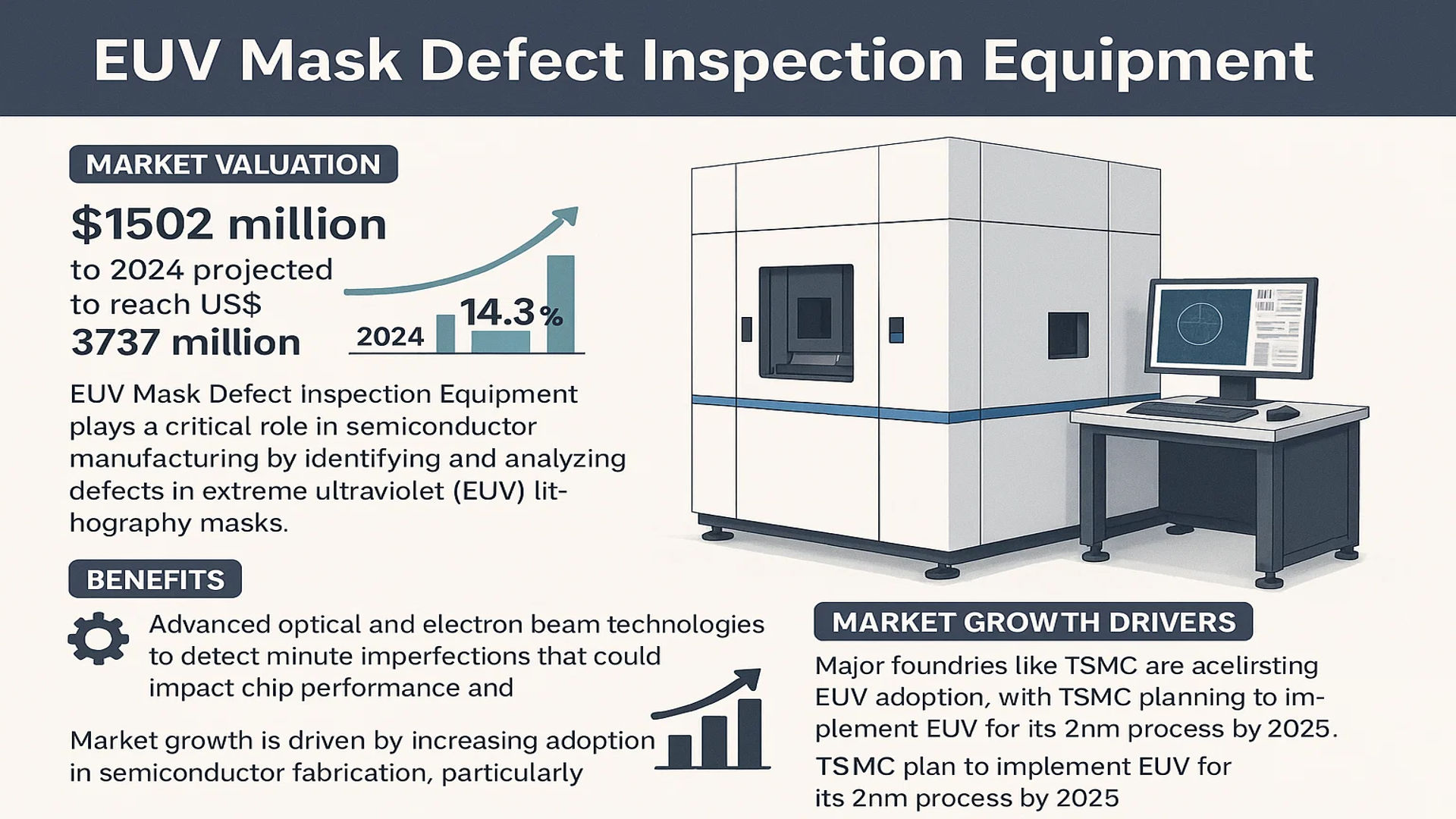
The global EUV Mask Defect Inspection Equipment Market was valued at 1502 million in 2024 and is projected to reach US$ 3737 million by 2032, at a CAGR of 14.3% during the forecast period.
EUV Mask Defect Inspection Equipment plays a critical role in semiconductor manufacturing by identifying and analyzing defects in extreme ultraviolet (EUV) lithography masks. These masks are essential for transferring circuit patterns onto silicon wafers with nanometer-scale precision, particularly in advanced process nodes below 7nm. The equipment utilizes advanced optical and electron beam technologies to detect minute imperfections that could impact chip performance and yield.
The market growth is driven by the increasing adoption of EUV lithography in semiconductor fabrication, particularly for cutting-edge applications in artificial intelligence, 5G, and high-performance computing. Major foundries like TSMC, Samsung, and Intel are accelerating their EUV adoption, with TSMC planning to implement EUV for its 2nm process by 2025. However, the market faces challenges including high equipment costs and technical complexities associated with detecting defects at such small scales. Lasertec and KLA currently dominate the market, holding over 90% combined share due to their technological leadership in high-resolution inspection systems.
MARKET DYNAMICS
MARKET DRIVERS
Advancements in Semiconductor Manufacturing Processes Fueling Demand for EUV Mask Inspection
The semiconductor industry’s relentless push towards smaller process nodes is creating unprecedented demand for EUV mask defect inspection equipment. As chipmakers transition to 5nm, 3nm, and below architectures, the tolerance for mask defects has shrunk dramatically – patterns that were acceptable at 28nm could now cause catastrophic failures. The precision required at these advanced nodes has made EUV mask inspection essential, with the market projected to grow at 14.3% CAGR through 2032. This growth is directly tied to the increasing complexity of semiconductor designs and the critical role masks play in pattern transfer accuracy.
Increased Adoption of EUV Lithography Systems Driving Equipment Investments
The semiconductor industry’s adoption of EUV lithography systems has accelerated significantly, with over 140 EUV systems installed worldwide as of 2024. Each new EUV scanner deployment creates immediate demand for matching inspection capabilities, as the masks used in these systems require specialized verification. The unique properties of EUV light – including its 13.5nm wavelength and absorption characteristics – demand inspection solutions that can effectively detect nanoscale defects without damaging the expensive masks. Major foundries are now requiring inspection capabilities that can identify defects as small as 16nm, pushing equipment manufacturers to continually enhance their detection technologies.
Growing Complexity of Mask Designs Necessitating Advanced Inspection Solutions
Modern EUV masks represent some of the most complex manufactured objects in existence, with multilayer structures comprising over 40 alternating silicon and molybdenum layers. The intricate nature of these masks, combined with the introduction of new technologies like inverse lithography and source-mask optimization, has dramatically increased the potential failure points. Current estimates suggest that a single critical defect on a 3nm process node mask could impact over 1,000 potential die locations, making comprehensive inspection not just desirable but essential for maintaining acceptable yields in high-volume manufacturing environments.
MARKET RESTRAINTS
Exorbitant Equipment Costs Creating Barriers to Market Entry
The development and manufacturing of EUV mask defect inspection systems represent one of the most capital-intensive segments in semiconductor equipment. A single high-end EUV inspection tool can cost upwards of $40 million, placing significant financial strain on both mask shops and foundries. These costs are compounded by the lengthy delivery times – currently stretching to 24 months for some systems – which creates challenges for capacity planning. For smaller semiconductor manufacturers and research institutions, these financial and time commitments may prove prohibitive, potentially limiting market growth in certain segments.
Technical Limitations in Detection Capabilities Restricting Adoption
While EUV mask inspection technology has advanced significantly, current systems still face challenges in detecting certain types of defects with the required sensitivity and speed. The industry is particularly concerned about phase defects – irregularities in the multilayer stack that don’t register as height variations but still affect imaging performance. Current inspection methods struggle to reliably identify all such defects while maintaining acceptable throughput. This creates a difficult balancing act for equipment developers who must simultaneously improve resolution, sensitivity, and inspection speed as process nodes continue to shrink.
Limited Availability of Skilled Personnel Constraining Market Expansion
The highly specialized nature of EUV mask inspection technology has created a severe shortage of qualified personnel across the semiconductor ecosystem. Operating and maintaining these systems requires expertise across multiple domains – including optics, photonics, materials science, and software algorithms. The talent gap is particularly acute in emerging semiconductor markets, where the rapid establishment of new fabs has outpaced the development of local technical expertise. This skills shortage represents a significant bottleneck for market growth, potentially delaying the full utilization of installed inspection capacity.
MARKET OPPORTUNITIES
Expansion of Domestic Semiconductor Production Creating New Demand
The global push for semiconductor supply chain resilience, exemplified by initiatives like the CHIPS Act in the United States and similar programs in Europe and Asia, is creating significant opportunities for EUV mask inspection equipment providers. With governments committing over $100 billion collectively to bolster domestic chip manufacturing, a wave of new fab construction is underway. Each new advanced node production facility will require dedicated EUV mask inspection capabilities, driving demand for both equipment and the specialized ancillary systems needed for full mask house operations. This represents a multi-year growth opportunity as these fabs move from construction to equipment installation phases.
Development of Next-Generation Inspection Technologies Opening New Markets
The ongoing evolution of inspection methodologies presents substantial growth potential for equipment innovators. Emerging techniques like actinic pattern inspection (API) and multi-beam inspection are showing promise in overcoming current resolution and throughput limitations. Companies that can commercialize these next-generation solutions stand to gain significant market share, particularly as the industry moves toward sub-2nm nodes where conventional inspection methods may prove inadequate. These technological advancements could also expand the market by enabling inspection for new applications such as advanced packaging and heterogeneous integration, where defect control is becoming increasingly critical.
Growth in Outsourced Semiconductor Assembly and Test (OSAT) Market Creating Additional Demand
The rapid expansion of the OSAT sector represents a significant opportunity for EUV mask inspection equipment providers. As packaging technologies become more sophisticated – incorporating techniques like wafer-level packaging and 3D IC stacking – the need for precise pattern transfer grows accordingly. While traditionally focused on less advanced nodes, leading OSAT providers are now investing in cutting-edge capabilities to support advanced packaging solutions. This transition creates demand for inspection equipment that can bridge the gap between front-end semiconductor manufacturing and back-end packaging requirements, opening new avenues for market expansion.
MARKET CHALLENGES
Supply Chain Vulnerabilities Threatening Equipment Production
The sophisticated nature of EUV mask inspection systems makes them particularly vulnerable to disruptions in the global supply chain. These machines incorporate thousands of precision components sourced from specialized suppliers worldwide, including high-end optics from Germany, precision stages from Japan, and advanced sensors from the United States. Geopolitical tensions and trade restrictions have made certain critical components difficult to procure, potentially delaying equipment deliveries. The situation is further complicated by the long lead times required for manufacturing and calibrating these systems, where even minor component shortages can result in significant production delays.
Intellectual Property Protection Concerns Limiting Collaboration
The highly proprietary nature of EUV mask inspection technologies has created an environment where knowledge sharing between companies is extremely limited. This secrecy, while understandable from a competitive standpoint, slows overall industry progress by preventing collaborative problem-solving. The challenge is particularly acute in addressing common technical hurdles like defect classification algorithms and system calibration methodologies. Without more open exchange of best practices, the industry risks duplicating efforts and wasting resources on solving problems that others may have already addressed.
Integration Challenges with Emerging Lithography Technologies
The potential introduction of next-generation lithography technologies, including high-NA EUV and nanoimprint lithography, presents significant integration challenges for inspection equipment providers. Each new lithography approach brings unique mask requirements and potential defect modes that existing inspection systems may not be optimized to detect. The industry faces the difficult task of developing flexible inspection platforms that can adapt to these emerging technologies while maintaining backward compatibility with existing processes. This balancing act requires substantial R&D investment and creates uncertainty about the long-term viability of current inspection methodologies.
EUV MASK DEFECT INSPECTION EQUIPMENT MARKET TRENDS
Increasing Adoption of Advanced Semiconductor Nodes to Drive Market Growth
The global semiconductor industry is witnessing rapid advancements in fabrication technologies, with foundries aggressively adopting EUV lithography for sub-7nm process nodes. As a critical enabler of these advanced nodes, EUV mask defect inspection equipment has become indispensable for maintaining production yields. The market is projected to grow at a 14.3% CAGR from 2024 to 2032, reaching $3.7 billion, driven by strong demand from leading-edge wafer fabs and mask shops. This growth trajectory reflects the industry’s transition towards next-generation 3nm and 2nm processes, where defect inspection precision becomes exponentially more critical.
Other Trends
Dual-Beam Inspection Technology Advancement
Manufacturers are developing hybrid inspection systems combining electron beam and optical technologies to address the unique challenges of EUV mask qualification. These systems offer superior defect detection capabilities, particularly for phase defects that conventional optical methods might miss. The recent introduction of multi-wavelength inspection platforms has improved sensitivity to sub-20nm defects while maintaining reasonable throughput speeds. Such innovations are crucial as defect tolerances tighten with each new process generation.
Shift Toward Fab-Based Inspection Solutions
While mask shops currently dominate EUV inspection equipment deployment with 61% market share in 2023, fabs are increasingly investing in their own inspection capabilities. This trend is fueled by the need for in-line monitoring of pellicle-protected masks and faster turn-around times. Advanced process control requirements at 3nm nodes are prompting fabs to integrate inspection systems directly into their production lines, with the fab segment expected to capture 42% of the market by 2030. Equipment manufacturers are responding with compact, high-throughput systems specifically designed for fab environments.
COMPETITIVE LANDSCAPE
Key Industry Players
Market Dominated by Specialized Semiconductor Inspection Leaders
The EUV mask defect inspection equipment market exhibits a highly concentrated competitive structure, with Lasertec Corporation and KLA-Tencor collectively controlling over 85% of the global market share as of 2024. This duopoly has emerged due to their proprietary technologies and deep expertise in EUV inspection methodologies, creating significant barriers to entry for new competitors.
Lasertec maintains its leadership position through continuous innovation in actinic (at-wavelength) inspection systems, which utilize EUV light sources to detect defects with unmatched precision. Their flagship EUV mask inspection systems are critical for advanced node development at leading foundries like TSMC, Samsung, and Intel. KLA-Tencor complements this with advanced optical inspection solutions and has strengthened its position through strategic R&D investments exceeding $1 billion annually in semiconductor process control technologies.
Meanwhile, Advantest Corporation represents the primary alternative with its electron-beam inspection capabilities. While currently holding a smaller market share, the company has been gaining traction through specialized solutions for emerging 3nm and below process nodes. Advanced semiconductor manufacturers increasingly adopt a hybrid approach, combining optical and e-beam inspection to maximize defect detection sensitivity across different mask layers.
The market’s technological intensity creates unique competitive dynamics. With equipment lead times extending beyond 24 months and system prices ranging between $30-50 million per unit, customers maintain long-term relationships with established suppliers. However, recent supply chain challenges have prompted some foundries to diversify their supplier base, creating opportunities for emerging competitors to develop alternative inspection solutions.
List of Key EUV Mask Defect Inspection Equipment Suppliers
- Lasertec Corporation (Japan)
- KLA Corporation (U.S.)
- Advantest Corporation (Japan)
- Applied Materials, Inc. (U.S.)
- ASML Holding NV (Netherlands)
- Hitachi High-Tech Corporation (Japan)
- Nikon Corporation (Japan)
- Carl Zeiss AG (Germany)
Segment Analysis:
By Type
3nm and Below Process Segment Leads Due to Rising Demand for Advanced Semiconductor Nodes
The market is segmented based on type into:
- 5-7nm Process
- 3nm and Below Process
By Application
Mask Shop Segment Dominates Owing to Critical Role in Initial Mask Qualification
The market is segmented based on application into:
- Mask Shop
- Fab
By Technology
Optical Inspection Holds Majority Share Due to High Throughput Capabilities
The market is segmented based on technology into:
- Optical Inspection
- Bright Field Inspection
- Dark Field Inspection
- SEM Inspection
By Equipment Type
Transmission Mode Systems Gain Traction for Enhanced Defect Detection
The market is segmented based on equipment type into:
- Reflection Mode Systems
- Transmission Mode Systems
- Hybrid Systems
Regional Analysis: EUV Mask Defect Inspection Equipment Market
Asia-Pacific
Asia-Pacific dominates the EUV Mask Defect Inspection Equipment market, driven by the concentrated semiconductor manufacturing hubs in Taiwan, South Korea, Japan, and China. Taiwan Semiconductor Manufacturing Company (TSMC), Samsung, and SK Hynix are aggressively expanding their EUV lithography capabilities, creating robust demand for high-precision inspection systems. China is making strategic investments to bolster domestic semiconductor production, though technical barriers remain. Japan remains critical for advanced materials and equipment supply chains, with Lasertec holding significant market share. While cost sensitivity exists in emerging economies, adoption is accelerating for 3nm and below process nodes, pushing regional CAGR above the global average.
North America
The U.S. leads North America’s market owing to substantial R&D investments and the presence of key fabless chip designers like Intel and AMD collaborating with equipment manufacturers. The CHIPS and Science Act has allocated $52 billion to strengthen domestic semiconductor infrastructure, indirectly benefiting inspection equipment demand. However, reliance on Asian foundries tempers short-term growth compared to APAC. KLA-Tencor’s dominance in California’s tech ecosystem supports innovation, particularly for multi-beam inspection solutions targeting sub-5nm defects. Regulatory pressures around export controls add complexity but reinforce local supply chain development.
Europe
Europe’s market is characterized by specialized equipment demand from ASML (Netherlands) and imec (Belgium), which pioneer EUV lithography research. While wafer fab capacity is limited compared to APAC, the region excels in developing cutting-edge inspection methodologies, particularly for photonmask metrology. EU-funded initiatives like the Chips Act aim to double Europe’s semiconductor share by 2030, yet the market remains constrained by high operational costs and fragmented production bases. Germany and the Netherlands are key revenue contributors, with collaborative projects between Carl Zeiss and ASML driving optical inspection advancements.
Middle East & Africa
This region shows nascent potential, primarily through strategic partnerships in Israel’s tech sector and UAE’s diversification efforts. Israel’s semiconductor design expertise creates peripheral demand for defect inspection in prototyping phases. However, the absence of large-scale fabs and reliance on imported equipment limit market penetration. Long-term opportunities may emerge if proposed mega-projects like Saudi Arabia’s NEOM integrate advanced manufacturing zones, but current adoption is marginal compared to global standards.
South America
South America remains a minor participant due to underdeveloped semiconductor ecosystems and limited EUV infrastructure. Brazil’s CEITEC and Argentina’s occasional R&D projects offer sporadic demand, but economic instability and reliance on legacy node technologies hinder meaningful market growth. The region primarily serves as an importer of finished chips rather than an inspection equipment consumer, with minimal local fab investments forecasted through 2032.
Report Scope
This market research report provides a comprehensive analysis of the Global EUV Mask Defect Inspection Equipment market, covering the forecast period 2025–2032. It offers detailed insights into market dynamics, technological advancements, competitive landscape, and key trends shaping the semiconductor lithography equipment industry.
Key focus areas of the report include:
- Market Size & Forecast: Historical data and future projections for revenue, unit shipments, and market value across major regions and segments. The market was valued at USD 1502 million in 2024 and is projected to reach USD 3737 million by 2032, growing at a CAGR of 14.3%.
- Segmentation Analysis: Detailed breakdown by process node (5-7nm and 3nm & below), application (Mask Shop vs Fab), and technology (optical vs SEM inspection) to identify high-growth segments.
- Regional Outlook: Insights into market performance across North America, Europe, Asia-Pacific, Latin America, and Middle East & Africa, with emphasis on semiconductor manufacturing hubs like Taiwan, South Korea, and Japan.
- Competitive Landscape: Profiles of dominant players Lasertec and KLA-Tencor (85% combined market share), their product roadmaps, manufacturing capacity, and technological innovations.
- Technology Trends: Assessment of EUV lithography advancements, integration of AI for defect classification, and emerging inspection methodologies for sub-3nm nodes.
- Market Drivers & Restraints: Evaluation of factors including semiconductor miniaturization trends, EUV adoption in advanced nodes, equipment lead times (up to 2 years), and high capital costs.
- Stakeholder Analysis: Strategic insights for semiconductor equipment manufacturers, foundries, IDMs, and investors regarding technology transitions and capacity expansions.
Research methodology combines primary interviews with industry experts, analysis of financial reports from key players, and validation through semiconductor manufacturing trend data to ensure accuracy and reliability.
FREQUENTLY ASKED QUESTIONS:
What is the current market size of Global EUV Mask Defect Inspection Equipment Market?
-> EUV Mask Defect Inspection Equipment Market was valued at 1502 million in 2024 and is projected to reach US$ 3737 million by 2032, at a CAGR of 14.3% during the forecast period.
Which key companies operate in this market?
-> Key players are Lasertec (Japan), KLA-Tencor (US), and Advantest (Japan), with Lasertec and KLA controlling 85% market share.
What are the key growth drivers?
-> Growth is driven by transition to 3nm/2nm nodes, increasing EUV adoption in foundries, and yield management requirements in advanced semiconductor manufacturing.
Which region dominates the market?
-> Asia-Pacific accounts for 78% market share, led by semiconductor manufacturing clusters in Taiwan, South Korea, and Japan.
What are the emerging trends?
-> Emerging trends include high-NA EUV inspection systems, AI-powered defect classification, and integrated metrology solutions for sub-3nm processes.

Get Sample Report PDF for Exclusive Insights
Report Sample Includes
- Table of Contents
- List of Tables & Figures
- Charts, Research Methodology, and more...


