Key Statistics
Key Takeaways
- IC manufacturing EPC is the largest and most technically demanding service segment because wafer fabs require contamination control, vibration isolation, ultrapure water, specialty gas and chemical systems, massive electrical loads, cleanroom HVAC and precise process-tool installation within one integrated facility.
- IC applications represent the largest end-use market because leading-edge logic, memory and mature-node fabs account for most greenfield semiconductor capital construction. Discrete, optoelectronic and sensor facilities remain important but generally require lower total project value per site.
- Asia Pacific is the largest regional market because most global wafer-fab capacity and the majority of new fab projects remain concentrated in Taiwan, South Korea, China, Japan and Southeast Asia. India is emerging as an additional high-growth EPC market through approved fab and OSAT investments.
- North America is the strongest localization-driven growth market. New U.S. fabs in Arizona, New York, Ohio and Texas are creating multi-year engineering, procurement, construction, tool-install and commissioning workloads while also forcing contractors to solve workforce, schedule and supply-chain constraints.
- Modularization and offsite manufacturing are becoming core delivery strategies. Bechtel has highlighted offsite modules, segmented construction sequencing and centralized procurement as methods to shorten semiconductor fab schedules, while Exyte and other specialists are applying BIM, digital twins and integrated project controls.
- Skilled-labor availability and utility integration are the principal delivery constraints. A fab requires large numbers of process-piping, electrical, mechanical, cleanroom and commissioning specialists plus long-lead equipment and utility systems. Project delivery capacity therefore depends on engineering and subcontractor networks as much as the balance sheet of the EPC contractor.
Engineering, Procurement and Construction (EPC) for Semiconductor Market Overview
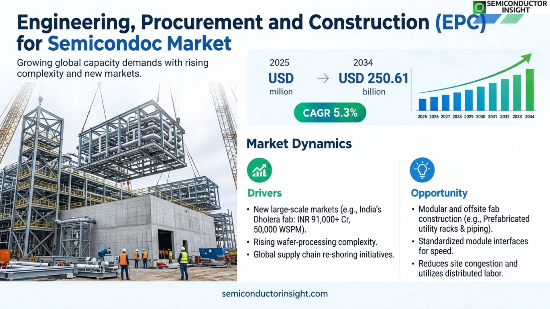
Engineering, Procurement and Construction (EPC) for Semiconductor Market was valued at USD 177.67 billion in 2025 and is projected to reach USD 250.61 billion by 2034, representing a 5.3% CAGR during 2026–2034. Asia Pacific is the largest regional market because most semiconductor wafer-fab and packaging capacity is concentrated there, while North America and India are creating major incremental EPC demand through manufacturing localization.
Semiconductor EPC covers the integrated engineering, procurement, construction, installation and commissioning services required to deliver semiconductor manufacturing facilities and related infrastructure. The work extends far beyond ordinary industrial construction. A fab must control airborne particles, vibration, humidity and temperature while supplying ultrapure water, specialty gases, chemicals, vacuum, exhaust, power and process cooling with extremely high reliability. Contractors must coordinate these systems with expensive production tools and with customer-specific cleanroom layouts.
The market includes three principal project types: semiconductor materials and equipment EPC, IC manufacturing EPC, and packaging and testing EPC. Each uses a different project-delivery model. Front-end IC fabs demand the highest cleanroom and utility sophistication; equipment and materials plants require specialized chemical, gas and process systems; packaging and testing facilities emphasize clean manufacturing, high-density electrical infrastructure, automation and rapid scale-up but generally use less extreme contamination control than leading-edge wafer fabs.
Project scale has increased as semiconductor companies localize capacity and move to more complex nodes. SEMI reported 18 new fab construction projects expected to start in 2025 and later projected about 50 new fabs coming online across 2025 and 2026. This creates overlapping demand for cleanroom engineering, process utilities, construction labor and commissioning resources across several countries at once, increasing the value of EPC firms with global procurement and subcontractor networks.
The commercial model is also moving toward programmatic relationships rather than one-off buildings. Large semiconductor customers expand a campus in phases, reuse standardized fab designs and expect EPC partners to support early planning, cost estimating, procurement, construction, tool installation and start-up. Exyte’s FabNext execution in Singapore, Bechtel’s semiconductor work in Clay, New York, Tata Projects’ semiconductor projects in India and SK ecoengineering’s integrated semiconductor EPC activities illustrate how contractors are building repeatable platforms around semiconductor-specific delivery.
Segment Analysis: By Type
By type, the market is segmented into Semiconductor Materials and Equipment EPC, IC Manufacturing EPC, and Packaging and Testing EPC. IC manufacturing EPC is the largest value segment because wafer fabs require the most complex cleanroom, utility and vibration-control systems and carry the highest project capital intensity. Packaging and testing EPC is expanding quickly as advanced packaging and OSAT capacity moves closer to front-end manufacturing.
| Type | Project scope | Market position |
|---|---|---|
| Semiconductor Materials and Equipment EPC | Covers facilities for semiconductor materials, specialty gases, chemicals, wafers, equipment production and supporting infrastructure. Projects may require high-purity process lines, hazardous-material controls, clean manufacturing spaces, precision utilities and specialized environmental systems. The commercial requirement is reliable process integration rather than the extreme patterning environment of a leading-edge wafer fab. | A strategic enabling segment. Growth follows localization of materials and equipment supply chains around major fab clusters. Customers value contractors that understand chemical handling, bulk gas systems, abatement, clean utilities and production equipment installation because these plants directly support fab continuity. |
| IC Manufacturing EPC | Includes front-end wafer fabs for logic, foundry, memory, analog, power and other integrated circuits. Scope can include civil works, shell, cleanroom, HVAC, ultrapure water, process cooling, specialty gases, chemicals, exhaust, power distribution, subfab systems, tool hook-up, automation and commissioning. | Largest and most complex segment. Leading-edge and memory fabs can be multi-billion-dollar programs with aggressive schedules and extremely tight environmental specifications. The customer’s ability to ramp wafer starts depends directly on facility completion, tool installation and utility stability. |
| Packaging and Testing EPC | Covers OSAT, advanced packaging, assembly and test plants, including clean manufacturing, high-density power and cooling, automation, process utilities and production-tool integration. Hybrid bonding, chiplet packaging and HBM-related assembly can require cleaner environments and more sophisticated process support than conventional packaging. | Fast-growing service segment. Advanced packaging investment is rising because AI accelerators and HBM move system performance into the package. India, the United States and Asia are adding packaging capacity, creating EPC demand that can often be delivered faster than a front-end fab but still requires semiconductor-grade project controls. |
Delivery model and modularization
A secondary market distinction is the project-delivery model. Customers may award a full EPC package, engineering and construction management, general-contractor scope, or multiple specialized work packages. Modular and offsite fabrication is expanding because utility racks, piping assemblies and selected structural systems can be built in parallel with site construction. Bechtel has described using offsite modules and segmented construction sequencing to accelerate semiconductor fab schedules, reducing congestion and moving labor to locations where it is more available.
Segment Analysis: By Application
By application, the market is segmented into ICs, Discrete Devices, Optoelectronic Devices, Sensors and Others. IC projects account for the largest EPC value because foundry, logic and memory fabs require the most capital-intensive facility systems. Discrete, optoelectronic and sensor facilities provide an important diversification base, particularly in automotive, power electronics, image sensing, RF and specialty semiconductor clusters.
| Application | Demand characteristics |
|---|---|
| ICs | Largest application. Logic, foundry, DRAM and NAND projects require the broadest cleanroom and process-utility scope and the largest tool-install workload. AI and high-performance computing are driving new leading-edge and memory capacity, while government incentives are adding geographic diversification. Contractors need deep experience in contamination control, vibration, utility redundancy and multi-phase campus expansion. |
| Discrete Devices | Power semiconductors, SiC, GaN, diodes and other discrete devices use front-end processing but often at mature or specialty nodes. EPC demand is driven by EV, renewable energy and industrial power electronics. Facilities may require epitaxy, high-temperature furnaces, implant, cleanroom and hazardous-material systems but can have different utility and vibration requirements from leading-edge logic. |
| Optoelectronic Devices | LED, laser, photonics and optical-device facilities require compound-semiconductor process utilities, clean environments and precision equipment integration. The market is smaller than ICs but can be engineering-intensive because materials such as GaAs, InP and GaN use specialty precursors and exhaust systems that demand experienced gas and chemical design. |
| Sensor | MEMS, image sensors and other sensor fabs combine front-end semiconductor processes with application-specific micromachining, packaging and test. Automotive, industrial and consumer sensing support steady demand. EPC contractors must adapt cleanroom and utility design to varied wafer sizes, specialty etch or deposition processes and high-volume test automation. |
| Others | Other projects include semiconductor research fabs, pilot lines, substrate plants and specialized electronics manufacturing. These facilities are often smaller but can have unusual process requirements. Research and pilot fabs also act as early qualification sites for future commercial nodes, giving specialized EPC firms opportunities to establish customer relationships before large-scale expansion. |
Regional Analysis
Asia Pacific is the largest semiconductor EPC market, North America has the strongest localization-driven growth, and Europe is expanding selectively through leading-edge, power and specialty semiconductor projects. The market follows fab construction rather than chip consumption. A region with high electronics demand but limited wafer manufacturing generates far less EPC revenue than a region building new fabs and packaging plants.
How does regional semiconductor EPC demand differ?
Asia Pacific combines the deepest semiconductor manufacturing base with established construction and specialty-subcontractor ecosystems. North America is adding greenfield capacity but faces materially higher labor and construction costs, making modularization and workforce planning critical. Europe has fewer projects but high technical complexity and regulatory requirements. India is emerging within Asia as a major new EPC opportunity, while South America and most of the Middle East & Africa remain selective, project-based markets.
| Region | Position | Growth outlook | Demand profile | What decides contractor selection |
|---|---|---|---|---|
| Asia Pacific | Largest | High | Foundry, memory, OSAT and localization led | Semiconductor track record, local subcontractors, schedule certainty, cleanroom expertise and cost |
| North America | Major growth market | Very high | Domestic fab localization and AI capacity led | Workforce strategy, modularization, procurement scale, cost control and advanced-node experience |
| Europe | Selective high-value market | Moderate to high | Leading-edge, automotive, power and specialty semiconductor led | Regulatory delivery, sustainability, cleanroom performance and cross-border supply coordination |
| South America | Nascent | Moderate from small base | Research, mature-node and electronics-industrial projects led | Project bankability, cost, local subcontractors and imported technical systems |
| Middle East & Africa | Emerging | Moderate from small base | Israel fabs and strategic diversification led | Ecosystem depth, utilities, technical workforce and technology-transfer feasibility |
Key Semiconductor EPC Contractors and Competitive Landscape
Competition is concentrated among contractors with proven semiconductor-fab experience because ordinary industrial-construction capability does not automatically translate into cleanroom and process-utility competence. Exyte, Bechtel and other global firms compete on program management, engineering integration, procurement leverage and international execution, while Asian and Chinese engineering groups bring local subcontractor access and strong domestic customer relationships.
The competitive advantage is increasingly organizational rather than purely technical. EPC contractors must manage thousands of design packages, long-lead equipment, specialty piping, cleanroom systems and simultaneous construction trades while maintaining strict safety and quality standards. Digital engineering, BIM, 4D scheduling and centralized project controls reduce rework and allow customers to see schedule or cost risk earlier. Contractors with standardized semiconductor design libraries can also reuse validated details across multiple fabs.
Regional contractors gain share when semiconductor investment moves into new markets because they can combine local construction knowledge with international process expertise. Tata Projects’ semiconductor wins in India and SK ecoengineering’s fab work in Korea and Indiana illustrate this pattern. China’s large domestic semiconductor build-out similarly supports state-owned and specialist local EPC organizations that can deliver civil, cleanroom and utility packages at scale.
Key Industry Players
- Exyte
- Bechtel
- Fluor Corporation
- CTCI
- Tata Projects
- SK ecoplant
- SAMSUNG E&A
- CESE2
- WISDRI
- Zhongdian Huanyu (Beijing) Construction Engineering Co., Ltd.
- China Construction First Building
- SEEDRI
- China Construction Third Engineering Bureau Co., Ltd.
- Shanghai Construction Group
Semiconductor EPC Project Delivery Capacity Analysis
For an EPC service market, effective capacity is the amount of semiconductor project work that contractors can engineer, procure, construct and commission simultaneously. The principal constraints are semiconductor-experienced engineers, cleanroom and process-utility subcontractors, field supervisors, long-lead equipment procurement and commissioning teams. A contractor can have a strong balance sheet and still be capacity-constrained if the required specialist workforce is committed to other fabs.
The global pipeline creates overlapping demand. SEMI reported 18 new fabs expected to start construction in 2025 and later projected about 50 new fabs coming online across 2025 and 2026. Projects are geographically dispersed, so EPC firms must duplicate project-management, procurement and field-support capability across several regions. This favors companies with established offices, standardized design systems and supplier frameworks in Asia, North America and Europe.
Offsite manufacturing expands delivery capacity by moving work away from congested fab sites. Bechtel has described semiconductor strategies that fabricate utility modules, piping assemblies and structural elements at external module yards while site construction proceeds in parallel. The approach can reduce dependence on local peak labor, improve quality control and shorten schedule, although it requires early design freeze and careful logistics planning.
Engineering digitalization also raises effective capacity. BIM, digital twins and 4D scheduling allow teams to coordinate cleanroom, utility and tool-install interfaces before physical construction. Exyte and Bechtel both emphasize integrated digital project delivery in semiconductor work. The commercial benefit is lower rework and a greater number of complex work packages managed by the same engineering organization without sacrificing schedule visibility.
Engineering, Procurement and Construction (EPC) for Semiconductor Market Dynamics
Market growth is driven by new fab construction, regional manufacturing incentives, AI-related semiconductor capacity and advanced packaging expansion. Growth is restrained by skilled-labor shortages, high construction costs, long permitting cycles and supply-chain bottlenecks. The strongest opportunities lie in modular fab delivery, standardized multi-fab campuses, advanced packaging plants, brownfield expansions and lifecycle services that continue after construction into tool installation, commissioning and facility operations.
MARKET DRIVERS
Drivers Impact Analysis*
| Market Factor | Directional Impact on CAGR Forecast* | Commercial Mechanism |
|---|---|---|
| Global fab localization and industrial incentives | +1.4 to +2.0 percentage points | New geographic capacity requires complete facilities, creating EPC demand even when equivalent manufacturing exists elsewhere. |
| AI, HBM and leading-edge capacity expansion | +1.0 to +1.5 percentage points | High-value logic and memory fabs require larger cleanrooms, denser utilities and complex tool-install programs. |
| Advanced packaging and OSAT investment | +0.7 to +1.1 percentage points | Chiplets, HBM and hybrid bonding are driving new packaging plants with semiconductor-grade clean manufacturing and utility requirements. |
Manufacturing localization creates entirely new project demand
A semiconductor company that adds capacity in a new country must build utilities, cleanrooms, support buildings and logistics infrastructure even if a similar fab already exists elsewhere. Government programs in the United States, Europe, Japan and India therefore multiply construction demand rather than simply shift it geographically. EPC firms benefit from both the new building and the need to establish local subcontractor, service and materials networks.
AI and HBM increase facility intensity
AI-related logic and memory plants require advanced equipment, dense process utilities, high electrical loads and tightly controlled cleanroom environments. HBM and advanced DRAM add new capacity and complex packaging requirements. The result is larger project value per fab and more specialized utility integration, increasing the amount of engineering and commissioning work captured by semiconductor-focused EPC firms.
India adds a new large-scale semiconductor construction market
India’s Dholera fab illustrates the scale of emerging-market EPC opportunity. The Government of India states that the project exceeds INR 91,000 crore and targets 50,000 wafer starts per month. Tata Projects has identified semiconductor facilities in Gujarat and Assam among its strategic wins, showing that localization can create both global and domestic EPC capability at the same time.
Fab expansions create recurring brownfield work
Semiconductor campuses rarely remain static. Customers add cleanroom bays, utility plants, tool sets and packaging capacity over multiple phases. Brownfield EPC can be more difficult than greenfield construction because production must continue while work is executed nearby. Contractors that understand an existing campus can therefore become long-term partners and capture recurring revenue through expansions, tool installation and facility modifications.
MARKET RESTRAINTS
Restraints Impact Analysis*
| Market Factor | Directional Impact on CAGR Forecast* | Commercial Mechanism |
|---|---|---|
| Skilled construction and engineering shortages | −0.9 to −1.4 percentage points | Multiple fab and data-center projects compete for cleanroom, electrical, mechanical, piping and commissioning specialists. |
| Higher construction costs outside established Asian hubs | −0.7 to −1.1 percentage points | Labor, materials, permitting and infrastructure can materially raise project cost and slow final investment decisions. |
| Long-lead procurement and utility equipment bottlenecks | −0.5 to −0.9 percentage points | Switchgear, transformers, pumps, air handling, specialty valves and process systems can have extended lead times that constrain schedule. |
Workforce is a binding constraint on simultaneous fab construction
Semiconductor projects need large numbers of electricians, pipefitters, welders, controls engineers, cleanroom installers and commissioning specialists. These same trades are also demanded by data centers, battery plants and other advanced-manufacturing projects. Contractors must invest in training, recruit across regions and use prefabrication to avoid schedule delays. If workforce availability cannot support a planned ramp, customers may phase projects or defer construction.
Western fab construction can carry a significant cost premium
Exyte has stated that semiconductor fab construction in Western markets can be at least 50% more expensive than in Asia for comparable facilities, driven by labor, materials, site preparation, utilities and permitting. High cost does not eliminate strategic projects, but it increases pressure on design standardization, modularization and incentive support. EPC firms must therefore prove total installed cost and schedule certainty rather than compete only on engineering sophistication.
Long-lead infrastructure can dictate the critical path
Fabs require large substations, transformers, chillers, air handlers, pumps, exhaust systems, specialty gas equipment and cleanroom components. Some items have lead times exceeding a year. Bechtel has highlighted centralized buying power as a way to improve procurement certainty. Contractors that fail to reserve critical equipment early can miss the customer’s tool move-in window even if civil construction remains on schedule.
MARKET OPPORTUNITIES
Modular and offsite fab construction
Utility racks, piping modules and selected structural systems can be fabricated offsite while site work progresses. This reduces congestion inside the fab shell and allows work to be performed where labor is available. The opportunity is strongest for contractors that standardize module interfaces and coordinate logistics early, because late design changes can eliminate the schedule advantage of prefabrication.
Standardized multi-fab campus designs
Large semiconductor manufacturers increasingly build repeated fab modules on one campus. Contractors can reuse cleanroom, utility and subfab designs, reducing engineering hours and procurement uncertainty. A validated standard also improves commissioning because operating teams encounter familiar systems across several buildings. EPC firms that help customers create repeatable design libraries can capture programmatic work across multiple phases.
Advanced packaging and hybrid-bonding facilities
AI accelerators and HBM are shifting value into advanced packaging, creating new plants for hybrid bonding, chiplets, substrate integration and testing. These projects need semiconductor-grade clean manufacturing, automation, high-density utilities and rapid ramp schedules. They can therefore expand the EPC addressable market beyond traditional front-end fabs and provide faster-turn projects for contractors with cleanroom expertise.
Lifecycle operations and facility optimization
The project relationship can continue after commissioning through facility management, water recycling, abatement, energy optimization and cleanroom upgrades. SK ecoplant’s sustainability strategy explicitly links semiconductor FAB construction with operational solutions such as water and air-treatment technologies. Lifecycle services create recurring revenue and deepen customer relationships beyond the one-time EPC contract.
Semiconductor EPC Supply Chain Analysis
The semiconductor EPC supply chain has four stages: design and project engineering, procurement of long-lead equipment and materials, construction and cleanroom installation, and commissioning plus tool hook-up. The stages are tightly linked because late equipment information can force redesign, while delayed utilities can stop tool qualification. The most successful EPC programs therefore integrate engineering, procurement and construction schedules rather than managing each discipline independently.
Stage 1 – Integrated engineering
Semiconductor design starts with process and equipment requirements rather than ordinary building geometry. Cleanroom classifications, vibration limits, utility redundancy and tool layouts drive the structural and MEP design. BIM and digital twins reduce clashes among dense systems. Early engineering quality determines whether modularization and early procurement are possible, so EPC firms increasingly bring construction and supplier input into the design phase rather than handing over completed drawings sequentially.
Stage 2 – Long-lead procurement and supplier management
Procurement can determine the project critical path. Electrical switchgear, transformers, air-handling units, process cooling, pumps, specialty valves and cleanroom materials may require commitments long before final installation. Large EPC firms use global purchasing frameworks and supplier relationships to reserve capacity. Semiconductor-specific procurement also includes ultra-clean piping, gas cabinets, chemical distribution and abatement equipment that require qualified vendors.
Stage 3 – Construction and contamination-controlled installation
Fab construction combines ordinary civil work with highly specialized cleanroom and process-utility installation. Once clean areas are established, work practices must control particles, welding contamination and material handling. Thousands of pipe and cable connections must be documented and tested. Quality failures can delay tool move-in, so contractors use extensive inspection and subcontractor controls rather than relying only on final commissioning.
Stage 4 – Tool installation and production readiness
A fab is commercially valuable only when process tools can run. Tool installation connects equipment to power, water, gases, chemicals, vacuum, exhaust and automation. The facility then undergoes leak testing, balancing, cleanliness certification and integrated commissioning. EPC firms with tool-install capability capture additional value and can shorten handoffs because the same project team coordinates facility and equipment interfaces.
Recent Developments in the Semiconductor EPC Market
At SEMICON West 2025 in Phoenix, Bechtel outlined the use of digital twins, 4D scheduling, offsite manufacturing, workforce development and programmatic supply-chain management to improve semiconductor fab project certainty. The focus reflects a market where contractors increasingly compete on schedule compression and execution systems rather than basic construction capacity.
SK ecoengineering reported that it is supporting SK hynix’s North American expansion and providing integrated EPC services for a semiconductor FAB in Indiana. The broader SK ecoplant group also highlights semiconductor FAB construction, the Yongin Semiconductor Cluster and operational solutions as core parts of its AI-infrastructure strategy.
India Semiconductor Mission, Tata Electronics and Tata Semiconductor Manufacturing signed a fiscal-support agreement for the Dholera project. The Government of India states that the fab involves more than INR 91,000 crore of investment and targets 50,000 wafer starts per month, creating a major cleanroom, process-utility and construction program in a new semiconductor region.
Exyte received the Singapore Project Management Institute’s top Engineering and Construction award for the FabNext project completed for Siltronic. The award category covers projects valued above SGD 200 million and highlights schedule, quality and execution performance-core differentiators in semiconductor EPC where delays directly postpone production revenue.
Tata Projects’ FY2024-25 annual report states that strategic wins included Tata Electronics’ semiconductor fabrication facilities in Assam and Gujarat. The disclosure is significant because it shows domestic Indian contractors building semiconductor-specific project experience alongside global EPC firms as India’s fab and packaging pipeline moves into execution.
REPORT SCOPE & SEGMENTATION
| Study Period | 2020–2034 |
| Base Year | 2025 |
| Estimated Year | 2026 |
| Forecast Period | 2026–2034 |
| Historical Period | 2020–2025 |
| Market Size 2025 | USD 177.67 Billion |
| Market Size 2034 | USD 250.61 Billion |
| Growth Rate | CAGR of 5.3% from 2026–2034 |
| Largest Market 2025 | Asia Pacific |
| Unit | Value (USD Million/Billion) |
| Segmentation | By Type, By Application and By Region |
| By Type | Semiconductor Materials and Equipment EPC · IC Manufacturing EPC · Packaging and Testing EPC |
| By Application | ICs · Discrete Devices · Optoelectronic Devices · Sensor · Other |
| By Region | North America · Europe · Asia Pacific · South America · Middle East & Africa |
| Companies Profiled | Exyte · Bechtel · Fluor Corporation · CTCI · Tata Projects · SK ecoplant · SAMSUNG E&A · CESE2 · WISDRI · Zhongdian Huanyu (Beijing) Construction Engineering Co., Ltd. · China Construction First Building · SEEDRI · China Construction Third Engineering Bureau Co., Ltd. · Shanghai Construction Group |
| Customization Scope | Country, regional, fab type, project stage, EPC package, contractor, cleanroom, process-utility and project-pipeline customization can be added for customer-specific market-entry and business-development requirements. |
Frequently Asked Questions
What is the size of the semiconductor EPC market in 2025?
The global engineering, procurement and construction market for semiconductor facilities was valued at USD 177.67 billion in 2025. It includes EPC activity for semiconductor materials and equipment plants, IC manufacturing fabs, and packaging and testing facilities.
What is the projected market size by 2034?
The market is projected to reach USD 250.61 billion by 2034, representing a 5.3% CAGR during 2026–2034. Growth is driven by new fab construction, regional manufacturing incentives, AI-related logic and memory investment, and advanced packaging expansion.
Which region leads semiconductor EPC demand?
Asia Pacific is the largest regional market because Taiwan, South Korea, China, Japan and Southeast Asia host most global semiconductor manufacturing capacity. India is emerging rapidly through approved fab and packaging projects, while North America has the strongest localization-driven growth.
Which EPC type is the largest?
IC manufacturing EPC is the largest and most technically complex segment because wafer fabs require advanced cleanrooms, ultrapure water, specialty gas and chemical systems, vibration control, high-reliability power, subfab infrastructure and intensive process-tool installation.
Which application creates the most EPC demand?
ICs account for the largest share because foundry, logic, DRAM and NAND fabs carry the highest project values. Discrete, optoelectronic and sensor facilities remain important, especially in automotive, power electronics, imaging and specialty semiconductor markets.
Why are semiconductor fabs difficult to build?
A fab combines strict contamination and vibration control with very large electrical, HVAC, ultrapure-water, gas, chemical, vacuum and exhaust systems. Thousands of process-tool connections must be installed and commissioned accurately. Small schedule or quality failures can delay production of extremely high-value semiconductor equipment.
How are EPC contractors shortening fab schedules?
Contractors are using offsite manufacturing, prefabricated utility modules, 4D scheduling, BIM, digital twins, early procurement and segmented construction. Bechtel has specifically highlighted offsite modules and alternative construction sequencing as methods to accelerate semiconductor fabs and reduce site congestion.
What are the main constraints on market growth?
The principal restraints are shortages of semiconductor-experienced engineers and skilled trades, high construction costs, long permitting and utility-development timelines, and long-lead equipment. Multiple fab and data-center projects can compete for the same electrical, mechanical and commissioning workforce.
Which companies are profiled in the report?
The report profiles Exyte, Bechtel, Fluor, CTCI, Tata Projects, SK ecoplant, SAMSUNG E&A, CESE2, WISDRI, Zhongdian Huanyu, China Construction First Building, SEEDRI, China Construction Third Engineering Bureau and Shanghai Construction Group.
What is the strongest long-term opportunity?
The strongest opportunities are modular fab construction, standardized multi-fab campus designs, advanced packaging facilities, brownfield expansions, tool-install services and lifecycle facility optimization. These services increase recurring EPC value beyond the initial building shell and cleanroom construction.

Get Sample Report PDF for Exclusive Insights
Report Sample Includes
- Table of Contents
- List of Tables & Figures
- Charts, Research Methodology, and more...
 Download Sample Report PDF