Embedded Die Packaging Market Insights
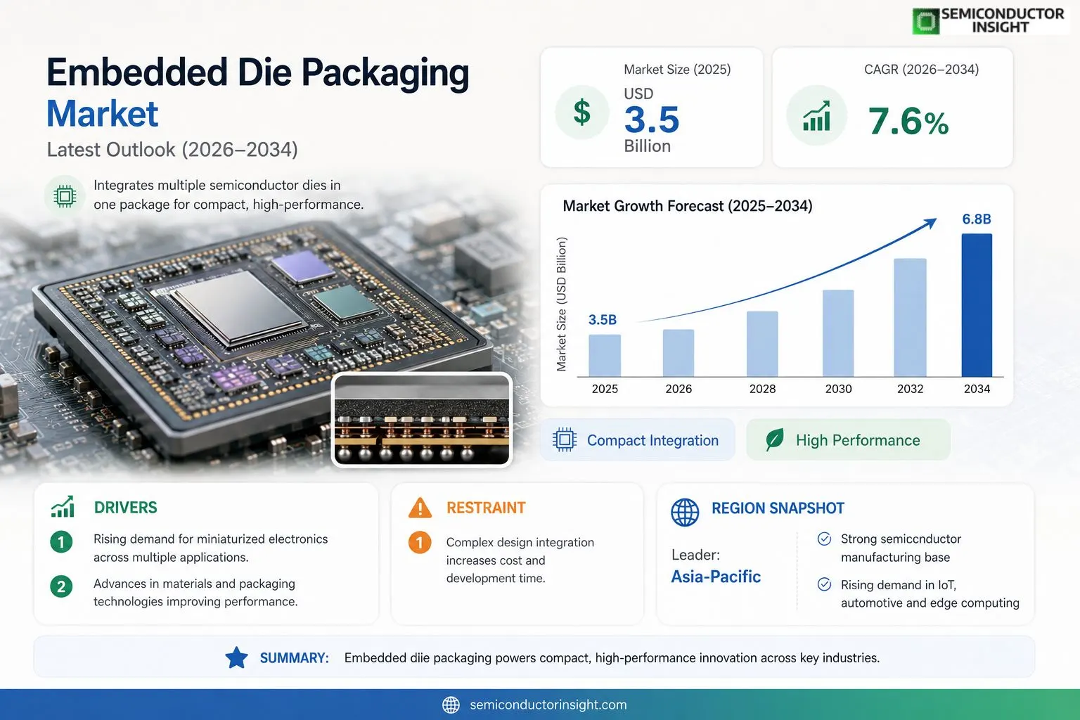
Global Embedded Die Packaging market size was valued at USD 3.5 billion in 2025. The market is projected to grow from USD 3.5 billion in 2025 to USD 6.8 billion by 2034, exhibiting a CAGR of 7.6% during the forecast period.
Embedded die packaging integrates multiple semiconductor dies within a single package substrate, enabling heterogeneous integration of logic, memory, RF and sensor functions while reducing footprint and improving performance metrics such as signal integrity and power efficiency.The market is accelerating because demand for compact high‑performance modules in IoT devices, automotive ADAS systems and edge‑computing continues to rise; however, challenges related to thermal management persist. Furthermore, advancements in fan‑out wafer‑level packaging (FOWLP) and silicon interposers are driving adoption, while leading players such as ASE Technology Holding, Amkor Technology, JCET Group and TSMC expand capacity through strategic investments.
MARKET DRIVERS
Increasing Demand for Miniaturized Electronics
Embedded Die Packaging Market is being propelled by the relentless push toward smaller, lighter electronic devices. Consumers expect smartphones, wearables, and medical sensors that occupy minimal board space while delivering higher performance, and embedded‑die solutions directly address this need through vertical integration.
Advancements in Materials and Process Technologies
Recent breakthroughs in low‑k dielectrics, copper‑pillar interconnects, and wafer‑level packaging have reduced parasitic losses and improved thermal management. These material innovations enable designers to adopt embedded die architectures without compromising reliability, thereby widening the addressable market.
➤ Industry analysts note that the convergence of 5G, automotive electronics, and edge‑AI creates a fertile environment for embedded die adoption, accelerating market growth beyond traditional consumer segments.
Overall, the synergy between consumer expectations for compactness and the availability of robust packaging technologies is a primary catalyst for Embedded Die Packaging Market expansion.
MARKET CHALLENGES
Complexity of Design Integration
Embedding dies requires precise alignment, advanced design‑for‑manufacturing (DFM) guidelines, and close collaboration between silicon designers and package engineers. This added complexity can extend development cycles and elevate engineering costs for many OEMs.
Other Challenges
Cost Sensitivity
The higher upfront investment in specialized tooling and material procurement makes cost‑sensitive customers hesitant, especially in price‑elastic markets such as consumer electronics where margins are thin.
MARKET RESTRAINTS
Supply Chain Volatility
Global shortages of high‑purity silicon wafers and advanced substrates have intermittently constrained production capacity, limiting the ability of suppliers to meet sudden spikes in demand for embedded solutions.In addition, the reliance on a limited number of specialized equipment manufacturers creates bottlenecks, making rapid scaling of new lines challenging for emerging entrants.Regulatory pressures concerning hazardous chemicals used in certain low‑k materials also impose compliance costs, further restraining market expansion.
MARKET OPPORTUNITIES
Growth in Automotive and IoT Segments
Electric vehicles, advanced driver‑assistance systems (ADAS), and connected IoT devices demand high‑density, reliable interconnects. Embedded die packaging offers the thermal performance and form‑factor advantages required for these safety‑critical applications.The rise of edge‑computing workloads, such as real‑time sensor fusion and on‑device AI inference, presents an opportunity for Embedded Die Packaging Market to deliver high‑speed, low‑latency solutions that traditional package‑on‑package architectures cannot match.Furthermore, manufacturers that invest in customized design services and rapid prototyping can capture niche markets seeking application‑specific embedded die solutions, unlocking additional revenue streams.
Embedded Die Packaging Market Trends
Demand for Compact High‑Performance Modules
Embedded Die Packaging Market is being driven by a surge in demand for compact, high‑performance modules across multiple end‑use sectors. IoT devices require integrated logic, memory, and sensor functions within a minimal footprint, prompting designers to adopt embedded die solutions that enhance signal integrity and power efficiency. Automotive advanced driver‑assistance systems (ADAS) also benefit from heterogeneous integration, allowing safety‑critical processors and radar/radio‑frequency components to coexist on a single substrate. Edge‑computing platforms similarly rely on reduced latency and lower power consumption, both of which are enabled by the tight coupling of dies that embedded die packaging provides. These application trends collectively reinforce the market’s momentum while highlighting the need for robust thermal management strategies.
Other Trends
Emerging Technologies and Process Innovations
Advancements in fan‑out wafer‑level packaging (FOWLP) and silicon interposer technologies are reshaping Embedded Die Packaging Market. FOWLP offers a cost‑effective route to high‑density interconnects, supporting the integration of diverse die types without the need for traditional substrate layers. Silicon interposers, meanwhile, deliver superior electrical performance and mechanical stability, making them attractive for high‑frequency and high‑power applications. Process innovations such as through‑silicon vias (TSVs) and advanced redistribution layers further improve thermal dissipation and mechanical reliability. Together, these technologies enable designers to overcome thermal constraints while delivering the miniaturization required by next‑generation devices.
Competitive Landscape and Capacity Expansion
Key players,including ASE Technology Holding, Amkor Technology, JCET Group, and TSMC,are expanding capacity to meet rising demand in Embedded Die Packaging Market. Strategic investments in new fab lines and equipment upgrades are aimed at scaling production while maintaining high yield rates. Partnerships with device manufacturers accelerate the co‑development of application‑specific solutions, reinforcing the competitive positioning of these foundries. The intensified focus on capacity and technology development is expected to sustain the market’s growth trajectory as customers seek reliable, high‑performance packaging options.
COMPETITIVE LANDSCAPEKey Industry Players
Global Embedded Die Packaging Market: Competitive Dynamics, Strategic Positioning, and Leading Manufacturer Profiles
Global embedded die packaging market is characterized by the strong presence of a few dominant players who collectively shape the industry’s technological and commercial direction. ASE Technology Holding, Amkor Technology, JCET Group, and TSMC stand out as frontrunners, leveraging their advanced packaging capabilities, expansive manufacturing infrastructure, and continued investment in fan-out wafer-level packaging (FOWLP) and silicon interposer technologies. These companies have strategically expanded their capacity to meet surging demand from IoT, automotive ADAS, and edge-computing segments. TSMC, in particular, has reinforced its leadership through its integrated fan-out (InFO) packaging platform, while ASE Technology Holding and Amkor Technology have deepened their competitive moats through diversified service portfolios and long-term customer partnerships across consumer electronics, telecommunications, and high-performance computing verticals. The market, valued at USD 3.5 billion in 2025 and projected to reach USD 6.8 billion by 2034 at a CAGR of 7.6%, reflects the intensifying competition among these key stakeholders to deliver heterogeneous integration solutions that optimize signal integrity, power efficiency, and form factor simultaneously.Beyond the tier-one leaders, several niche and regionally significant players are gaining competitive traction within the embedded die packaging ecosystem. Companies such as Intel Corporation and Samsung Electronics are driving innovation through proprietary embedded multi-die interconnect bridge (EMIB) and fan-out panel-level packaging (FOPLP) technologies respectively, targeting high-performance computing and mobile applications. AT&S, Shinko Electric Industries, and Ibiden Co., Ltd. are establishing strong footholds as substrate-centric specialists, supplying advanced embedded die substrates to leading semiconductor assemblers. Meanwhile, Nepes Corporation, Unimicron Technology, and Toppan Inc. are expanding their embedded die packaging capabilities to address thermal management challenges and heterogeneous integration requirements across automotive and industrial end markets. Siliconware Precision Industries (SPIL), now integrated under the ASE Group, further consolidates market share, while emerging players including Deca Technologies continue to disrupt the competitive landscape through innovative adaptive patterning processes that enhance yield and scalability across high-volume production environments.
List of Key Embedded Die Packaging Companies Profiled
- ASE Technology Holding Co., Ltd.
- Amkor Technology, Inc.
- JCET Group Co., Ltd.
- Taiwan Semiconductor Manufacturing Company (TSMC)
- Intel Corporation
- Samsung Electronics Co., Ltd.
- AT&S Austria Technologie & Systemtechnik AG
- Shinko Electric Industries Co., Ltd.
- Ibiden Co., Ltd.
- Nepes Corporation
- Unimicron Technology Corporation
- Toppan Inc.
- Siliconware Precision Industries Co., Ltd. (SPIL)
- Deca Technologies Inc.
- Powertech Technology Inc.
Segment Analysis:
| Segment Category | Sub-Segments | Key Insights |
| By Type |
|
System‑in‑Package is emerging as the leading type because it enables heterogeneous integration while preserving a compact footprint. – Designers value the flexibility to combine logic, memory and RF dies within a single substrate, which shortens time‑to‑market. – The architecture supports incremental upgrades, allowing manufacturers to respond quickly to evolving functionality demands. – Robust signal‑integrity characteristics make SiP especially attractive for high‑performance edge‑computing modules. |
| By Application |
|
Internet of Things drives the dominant application scenario due to the relentless push for miniature yet capable modules. – Embedded die solutions satisfy the need for low power consumption while delivering sufficient processing capability. – The ability to integrate sensors, connectivity and computation in a single package accelerates product differentiation for wearables and smart‑home gadgets. – OEMs favor the reduced bill‑of‑materials and simplified board layout that embedded die packaging provides. |
| By End User |
|
Device manufacturers emerge as the primary end‑user because they directly seek to embed multiple functions within constrained volumes. – They prioritize design‑time efficiencies and the ability to consolidate component count. – Close collaboration with packaging partners enables rapid iteration on thermal‑management strategies. – The visibility of improved reliability and reduced failure rates strengthens their preference for embedded die solutions. |
| By Integration Technology |
|
Silicon interposer leads this category because it offers a high‑density interconnect platform that supports diverse die sizes. – The technology excels at preserving signal integrity for high‑speed interfaces. – It facilitates efficient thermal pathways, addressing a key challenge in densely packed modules. – Industry players are investing in advanced lithography to improve interposer yield and cost‑effectiveness. |
| By Performance Requirement |
|
Low‑power operation dominates the performance narrative as many target applications demand extended battery life. – Embedded die architectures allow power gating of individual dies, significantly curbing standby consumption. – The consolidated footprint reduces parasitic losses, contributing to overall efficiency. – Designers often pair low‑power dies with advanced substrate materials that further mitigate thermal buildup. |
Regional Analysis: North America
United States
The primary drivers in the United States market include the expansion of the AI sector, growing demand for high-bandwidth connectivity, and the increasing adoption of advanced semiconductor packaging techniques for automotive and industrial applications.
Ongoing advancements in 3D packaging, fan-out wafer-level packaging (FOWLP), and chiplets are significantly influencing Embedded Die Packaging Market in the US, enabling higher integration density and improved performance.
The US market features a highly competitive landscape with established players and emerging startups vying for market share, focusing on innovation and customized solutions to meet specific customer needs.
The future of Embedded Die Packaging Market in the US is expected to be shaped by the increasing adoption of heterogeneous integration and the growing demand for power-efficient packaging solutions.
Europe
Europe is witnessing steady growth in Embedded Die Packaging Market, driven by a strong emphasis on industrial automation, automotive electronics, and the burgeoning electric vehicle sector. Several countries, particularly Germany, France, and the UK, are investing heavily in advanced manufacturing capabilities, which is bolstering the demand for sophisticated packaging solutions. While the pace of adoption might be slightly slower compared to the US, Europe presents a significant and evolving opportunity for embedded die packaging vendors.
Asia-Pacific
Asia-Pacific is the fastest-growing region in Embedded Die Packaging Market, spearheaded by China, Japan, and South Korea. The region’s dominance in semiconductor manufacturing and its large consumer electronics market are key factors driving this expansion. The increasing demand for advanced packaging in smartphones, wearables, and automotive electronics is fueling the growth of this market. Stringent government policies supporting domestic semiconductor industries further contribute to the region’s rapid development in embedded die packaging.
South America
South America represents a nascent market for Embedded Die Packaging Market, albeit with potential for future growth. The expanding telecommunications infrastructure and increasing adoption of IoT devices in countries like Brazil and Argentina are creating demand for advanced packaging solutions. However, the market is currently characterized by moderate investment and a reliance on imports.
Middle East & Africa
The Middle East & Africa region presents a relatively small but growing market for Embedded Die Packaging. The increasing investment in infrastructure projects, particularly in the telecommunications and energy sectors, is driving demand for reliable and high-performance electronic components. The region’s growing focus on technology and digital transformation is expected to further fuel the adoption of embedded die packaging in the coming years.
Report Scope
This market research report provides a comprehensive analysis of the Embedded Die Packaging Market , covering the forecast period 2026–2034. It offers detailed insights into market dynamics, technological advancements, competitive landscape, and key trends shaping the industry.
Key focus areas of the report include:
- Market Overview: The report begins with an overview outlining its current market scenario, key growth indicators, and industry transformation drivers. It discusses macroeconomic factors, demand–supply balance, regulatory landscape, and the strategic role of semiconductors in powering advancements across industries such as automotive, telecommunications, consumer electronics, and industrial automation.
- Market Size & Forecast: Historical data and future projections for revenue, unit shipments, and market value across major regions and segments.
- Segmentation Analysis: Detailed breakdown by product type, technology, application, and end-user industry to identify high-growth segments and investment opportunities.
- Regional Insights: Insights into market performance across North America, Europe, Asia-Pacific, Latin America, and the Middle East & Africa, including country-level analysis where relevant.
- Competitive Landscape: Profiles of leading market participants, including their product offerings, R&D focus, manufacturing capacity, pricing strategies, and recent developments such as mergers, acquisitions, and partnerships.
- Technology Trends & Innovation: Assessment of emerging technologies, integration of AI/IoT, semiconductor design trends, fabrication techniques, and evolving industry standards.
- Market Drivers & Restraints: Evaluation of factors driving market growth along with challenges, supply chain constraints, regulatory issues, and market-entry barriers.
- Stakeholder Insights: Insights for component suppliers, OEMs, system integrators, investors, and policymakers regarding the evolving ecosystem and strategic opportunities.
Primary and secondary research methods are employed, including interviews with industry experts, data from verified sources, and real-time market intelligence to ensure the accuracy and reliability of the insights presented.
FREQUENTLY ASKED QUESTIONS:
What is the current market size of Embedded Die Packaging Market?
-> Global Embedded Die Packaging Market was valued at USD 3.5 billion in 2025 and is expected to reach USD 6.8 billion by 2034, exhibiting a CAGR of 7.6% during the forecast period.
Which key companies operate in Embedded Die Packaging Market?
-> Key players include ASE Technology Holding, Amkor Technology, JCET Group and TSMC, among others.
What are the key growth drivers?
-> Key growth drivers include demand for compact high‑performance modules in IoT devices, automotive ADAS systems and edge‑computing, as well as advancements in fan‑out wafer‑level packaging (FOWLP) and silicon interposers.
Which region dominates the market?
-> Asia-Pacific is emerging as the fastest‑growing region, while North America remains a dominant market due to strong semiconductor manufacturing ecosystems.
What are the emerging trends?
-> Emerging trends include heterogeneous integration of logic, memory, RF and sensor functions within a single substrate, and increasing focus on thermal management solutions for high‑density packages.

Get Sample Report PDF for Exclusive Insights
Report Sample Includes
- Table of Contents
- List of Tables & Figures
- Charts, Research Methodology, and more...
 Download Sample Report PDF