Dummy Wafers Market Insights
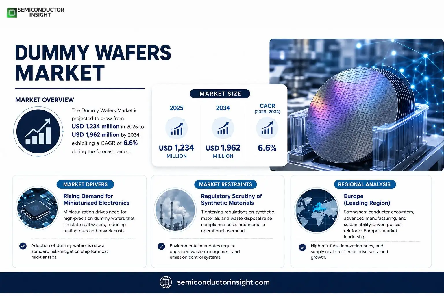
Dummy Wafers market size was valued at USD 1234 million in 2025. The market is projected to grow from USD 1234 million in 2025 to USD 1962 million by 2034, exhibiting a CAGR of 6.6% during the forecast period.
A dummy wafer is a core class of fab “non‑product wafers” used for slot filling, protection, stabilization and verification rather than shipment. In batch furnaces and certain deposition/diffusion operations dummy wafers act as filler wafers to satisfy loading requirements and help stabilize thermal/gas environments; they also serve as seasoning/conditioning wafers after maintenance or recipe changes and as sacrificial carriers for handling, transport and mechanical evaluations.Dummy wafers follow two primary supply routes: silicon‑based waferseither virgin test‑grade silicon or reclaimed wafers that are stripped, polished and cleanedand long‑life non‑silicon variants such as SiC or quartz that endure high‑temperature cycling and frequent cleaning, thereby reducing replacement frequency and total cost.
MARKET DRIVERS
Rising Demand for Miniaturized Electronics
Manufacturers of consumer and industrial devices are compressing circuitry to achieve lighter, more portable products. This compression creates a direct need for high‑precision dummy wafers that simulate real silicon during early‑stage testing, reducing costly re‑work later in the production line.
Cost‑Efficiency Pressures in Semiconductor Fabrication
Foundries are tightening budgets as yield improvements plateau. Incorporating dummy wafers into the process flow enables batch‑level verification without consuming expensive functional dies, allowing firms to preserve valuable silicon inventory for final qualification.
➤ Adoption of dummy wafers is now a standard risk‑mitigation step for most mid‑tier fabs.
Overall, the convergence of product miniaturization and tighter cost controls is compelling equipment suppliers to expand their dummy wafer portfolios, which in turn fuels incremental revenue streams across the supply chain.
MARKET CHALLENGES
Limited Availability of Specialty Substrate Materials
Some high‑frequency applications require rare substrate compositions that are not produced at scale. The scarcity forces customers to source bespoke dummy wafers, driving up lead times and price premiums.
Other Challenges
Integration Complexity
Embedding dummy wafers into existing process lines often demands custom tooling, which can interrupt production schedules and require additional engineering resources.Moreover, the need for precise alignment between dummy and functional wafers adds a layer of procedural oversight that smaller manufacturers may find difficult to sustain without dedicated support.
MARKET RESTRAINTS
Regulatory Scrutiny of Synthetic Materials
Authorities in several regions are tightening guidelines around the disposal and handling of synthetic silicon analogues. Companies must invest in compliance programmes, which adds overhead and can deter smaller players from entering the market.Environmental mandates are also prompting revisions to waste‑management protocols, meaning that manufacturers need to redesign back‑end processes to meet stricter emission thresholds.
MARKET OPPORTUNITIES
Expansion into Advanced Packaging
As 3D‑IC and heterogeneous integration mature, test engineers are seeking dummy wafers that can emulate multi‑die stacks. Suppliers that can deliver tailored thickness and carrier configurations stand to capture a growing share of the advanced packaging ecosystem.Parallel growth in automotive electronics, where reliability testing is non‑negotiable, presents a parallel avenue for providers to differentiate through ruggedized dummy wafer solutions designed for high‑temperature environments.
Dummy Wafers Market Trends
Shift Toward Long‑Life Non‑Silicon Dummy Wafers
Fab operators are increasingly favoring SiC and quartz‑based dummy wafers for high‑temperature and frequent‑clean cycles. These materials resist thermal shock and chemical attack far better than reclaimed silicon, allowing changeover intervals to extend beyond three years in many PECVD and diffusion tools. The extended lifespan translates directly into higher tool availability, because fewer wafer swaps mean less downtime for loading and conditioning. For equipment manufacturers, the trend creates an opportunity to market auxiliary services such as customized coating or surface‑polishing that preserve the durability advantage of these long‑life wafers. Consequently, Dummy Wafers Market is seeing a reallocation of spend from low‑cost reclaimed silicon toward premium, durability‑focused offerings.
Other Trends
Supply‑Chain Realignment Around Reclaimed Silicon Services
While SiC and quartz dominate niche high‑stress applications, the bulk of wafer loading still relies on reclaimed silicon wafers. Recent consolidations among reclaim specialists have tightened the supply chain, resulting in more standardized cleaning and polishing protocols. Fab managers benefit from predictable thickness loss per reclaim cycle, which simplifies inventory planning and reduces the risk of thin‑wafer failures. At the same time, service providers are adding value‑added steps such as thin‑film deposition or oxide passivation to differentiate their reclaimed products. This shift encourages fabs to negotiate longer‑term contracts, aligning cost structures with the anticipated lifespan of reclaimed wafers and smoothing the cash flow for both suppliers and end users.
Integration of Dummy Wafer Usage into Factory Automation Strategies
Modern fabs are embedding dummy wafer handling into their overall automation workflows. Sensors now track wafer thickness and surface condition in real time, prompting automatic swaps when a wafer approaches its end‑of‑life threshold. This data‑driven approach reduces manual inspection time and minimizes the probability of loading a wafer that could destabilize the thermal profile of a batch furnace. Moreover, by linking dummy wafer status to overall equipment effectiveness (OEE) metrics, production planners can quantify the contribution of filler and seasoning wafers to overall throughput. The result is a more transparent cost‑benefit analysis that informs decisions about whether to invest in longer‑life materials or to optimise reclaim cycles.
COMPETITIVE LANDSCAPE
Key Industry Players
Dummy Wafers Market: Competitive Overview
The silicon‑based dummy wafer segment remains anchored by a handful of vertically integrated manufacturers. Shin‑Etsu Chemical and SUMCO leverage expansive crystal‑growth capacity and sophisticated reclamation loops to supply both virgin test‑grade silicon and reclaimed wafers that have been stripped, polished and re‑certified. Their breadth of process control enables consistent thickness tolerances, which in turn stabilizes furnace loading and reduces cycle‑time variability for fabs. Wafers and Siltronic AG complement this tier by offering premium silicon products aimed at high‑volume front‑end customers, while also operating dedicated cleaning services that extend wafer life. This concentration of capabilities creates a de‑facto supply hierarchy: large silicon growers dominate the bulk market, whereas mid‑size firms specialize in value‑added reclaim services, shaping pricing power and influencing fab scheduling decisions.Beyond the silicon core, specialty providers carve out distinct niches through material innovation. Entegris markets SiC‑based SUPERSiC wafers that survive repeated high‑temperature cycles, positioning them as cost‑saving alternatives to frequently replaced silicon blanks. Heraeus’ Black Quartz HBQ® line targets furnace deposition where thermal‑expansion matching is critical, offering durability in aggressive cleaning regimes. RS Technologies, Kinik and Phoenix Silicon International focus on precision‑reclaimed dummy and monitor wafers, often bundling film‑coating or surface‑treatment options to meet specific process windows. These firms differentiate by extending wafer service life, reducing change‑over frequency, and thereby enhancing overall equipment effectiveness. Their strategies illustrate a parallel market track that competes on longevity and material resilience rather than sheer volume.
List of Key Dummy Wafers Companies Profiled
- Shin‑Etsu Chemical
- SUMCO
- Wafers
- Siltronic AG
- SK Siltron
- FST Corporation
- Wafer Works Corporation
- National Silicon Industry Group (NSIG)
- Entegris
- Heraeus
- RS Technologies
- Kinik
- Phoenix Silicon International
- Hangzhou Lion Microelectronics
- Shanghai Advanced Silicon Technology (AST)
Segment Analysis:
| Segment Category | Sub-Segments | Key Insights |
| By Type |
|
Reclaimed Silicon Dummy Wafer
|
| By Application |
|
Furnace Loading / Filling
|
| By End User |
|
Foundries
|
| By Technology |
|
Batch Furnace Processing
|
| By Service Model |
|
Reclaim & Refurbish Programs
|
Regional Analysis: Dummy Wafers Market
Europe
The European wafer ecosystem is anchored by high‑mix, low‑volume production lines that thrive on customization. Facilities in the Benelux region excel at rapid tooling changes, enabling customers to trial new device architectures without extensive re‑tooling. This flexibility feeds a steady demand for dummy wafers that replicate final product geometries, allowing process engineers to fine‑tune lithography steps early in the development cycle.
Recent geopolitical shifts have prompted European firms to diversify upstream sources. By sourcing silicon blocks from multiple EU members, manufacturers mitigate the risk of single‑point failures. This approach dovetails with a growing trend toward inventory buffers of dummy wafers, ensuring that critical test phases proceed unhindered even when external logistics encounter delays.
The EU’s circular‑economy directives incentivize the reuse of wafer substrates. Companies that adopt recyclable dummy wafers can claim lower carbon footprints, a factor increasingly weighed by procurement committees. This policy pressure nudges suppliers toward higher‑purity silicon grades that sustain repeated thermal cycles without degradation.
Innovation clusters around Munich and Eindhoven host joint labs where dummy wafer manufacturers test novel surface coatings. These collaborations translate into faster adoption of anti‑reflective layers that improve lithographic yield, a subtle advantage that can swing competitive positioning in downstream device markets.
North America
North America remains a sizable consumer of dummy wafers, driven by its expansive semiconductor foundry footprint in the United States and Canada. Customer priorities centre on speed‑to‑market; as a result, vendors focus on just‑in‑time delivery models that align with aggressive product launch schedules. The region’s emphasis on advanced packaging also raises demand for dummy wafers that mimic multi‑die stacking, supporting test engineers in validating interconnect reliability before full‑scale production.
Asia‑Pacific
In Asia‑Pacific, rapid capacity expansion across China, South Korea, and Taiwan fuels a burgeoning need for dummy wafers that can accommodate large‑diameter equipment. Local manufacturers are investing in automation to reduce manual handling, a move that improves repeatability and shortens cycle times. Cultural emphasis on cost efficiency drives the adoption of lower‑cost dummy wafer variants, albeit with stringent quality controls to meet high‑volume fab standards.
South America
South America’s market for dummy wafers is still nascent, constrained by limited domestic fabrication capacity. However, recent government incentives aimed at establishing micro‑electronics parks in Brazil and Chile have sparked interest among multinational suppliers. These initiatives are expected to create a modest but steady demand for dummy wafers that can serve pilot lines and technology‑transfer projects.
Middle East & Africa
The Middle East & Africa region exhibits a tentative entry into the dummy wafer space, largely through joint ventures with European firms seeking to tap emerging opportunities. Investment in renewable‑energy‑driven data centres is spurring a peripheral demand for semiconductor components, which indirectly raises awareness of the testing substrates required to qualify such components. Market participants view the region as a long‑term growth frontier, contingent on infrastructure development and skilled‑labor pipelines.
Report Scope
This market research report provides a comprehensive analysis of the Dummy Wafers Market , covering the forecast period 2026–2034. It offers detailed insights into market dynamics, technological advancements, competitive landscape, and key trends shaping the industry.
Key focus areas of the report include:
- Market Overview: The report begins with an overview outlining its current market scenario, key growth indicators, and industry transformation drivers. It discusses macroeconomic factors, demand–supply balance, regulatory landscape, and the strategic role of semiconductors in powering advancements across industries such as automotive, telecommunications, consumer electronics, and industrial automation.
- Market Size & Forecast: Historical data and future projections for revenue, unit shipments, and market value across major regions and segments.
- Segmentation Analysis: Detailed breakdown by product type, technology, application, and end-user industry to identify high-growth segments and investment opportunities.
- Regional Insights: Insights into market performance across North America, Europe, Asia-Pacific, Latin America, and the Middle East & Africa, including country-level analysis where relevant.
- Competitive Landscape: Profiles of leading market participants, including their product offerings, R&D focus, manufacturing capacity, pricing strategies, and recent developments such as mergers, acquisitions, and partnerships.
- Technology Trends & Innovation: Assessment of emerging technologies, integration of AI/IoT, semiconductor design trends, fabrication techniques, and evolving industry standards.
- Market Drivers & Restraints: Evaluation of factors driving market growth along with challenges, supply chain constraints, regulatory issues, and market-entry barriers.
- Stakeholder Insights: Insights for component suppliers, OEMs, system integrators, investors, and policymakers regarding the evolving ecosystem and strategic opportunities.
Primary and secondary research methods are employed, including interviews with industry experts, data from verified sources, and real-time market intelligence to ensure the accuracy and reliability of the insights presented.
FREQUENTLY ASKED QUESTIONS:
What is the current market size of Dummy Wafers Market?
-> Dummy Wafers Market was valued at USD 1234 million in 2025 and is expected to reach USD 1962 million by 2034 at a CAGR of 6.6%.
Which key companies operate in Dummy Wafers Market?
-> Key players include Shin-Etsu Chemical, SUMCO, Wafers, Siltronic AG, SK Siltron, FST Corporation, Wafer Works Corporation, National Silicon Industry Group (NSIG), Zhonghuan Advanced Semiconductor Materials, Hangzhou Lion Microelectronics, Hangzhou Semiconductor Wafer, GRINM Semiconductor Materials, Shanghai Advanced Silicon Technology (AST), Xi’an ESWIN Material Technology, RS Technologies, Kinik, Phoenix Silicon International, Hamada Rectech, Mimasu Semiconductor Industry, GST, Scientech, Pure Wafer, TOPCO Scientific Co. LTD.
What are the key growth drivers?
-> Key growth drivers include the need for furnace filler/loading stabilization, post‑maintenance conditioning, recipe‑change verification, and cost‑effective wafer reuse through reclamation and long‑life SiC/quartz technologies.
Which region dominates the market?
-> Asia dominates Dummy Wafers Market due to the high concentration of semiconductor manufacturing facilities, with significant demand in China, Japan, and South Korea.
What are the emerging trends?
-> Emerging trends include adoption of long‑life SiC dummy wafers, quartz‑based filler wafers, increased recycling of reclaimed silicon wafers, and development of specialty coated wafers for high‑temperature processes.
Get Sample Report PDF for Exclusive Insights
Report Sample Includes
- Table of Contents
- List of Tables & Figures
- Charts, Research Methodology, and more...
 Download Sample Report PDF