MARKET INSIGHTS
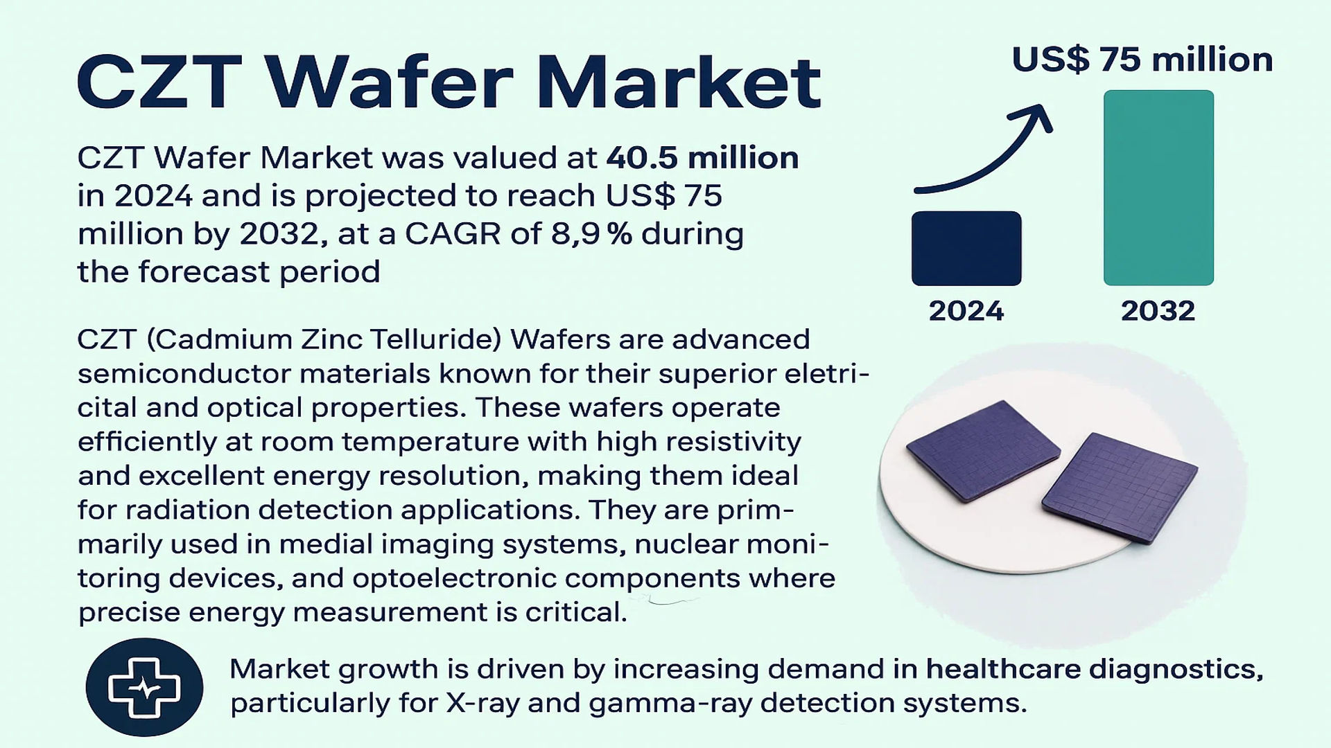
The global CZT Wafer Market was valued at 40.5 million in 2024 and is projected to reach US$ 75 million by 2032, at a CAGR of 8.9% during the forecast period.
CZT (Cadmium Zinc Telluride) Wafers are advanced semiconductor materials known for their superior electrical and optical properties. These wafers operate efficiently at room temperature with high resistivity and excellent energy resolution, making them ideal for radiation detection applications. They are primarily used in medical imaging systems, nuclear monitoring devices, and optoelectronic components where precise energy measurement is critical.
Market growth is driven by increasing demand in healthcare diagnostics, particularly for X-ray and gamma-ray detection systems. The expanding nuclear medicine sector and rising security applications in defense are additional growth factors. Technological advancements in wafer manufacturing processes and the development of large-area CZT crystals are further propelling market expansion. Key manufacturers are investing in R&D to improve crystal quality and reduce production costs, which could accelerate adoption across emerging applications.
MARKET DYNAMICS
MARKET DRIVERS
Growing Demand for Advanced Medical Imaging to Accelerate CZT Wafer Adoption
The global healthcare sector’s increasing reliance on precise diagnostic tools is fueling demand for cadmium zinc telluride (CZT) wafers. These semiconductor materials exhibit superior energy resolution and room-temperature operability, making them ideal for SPECT, PET, and gamma-ray detection systems. The medical imaging market, valued at over $35 billion, is projected to grow at 6% CAGR through 2030, with CZT-based detectors gaining prominence due to their ability to reduce patient radiation exposure by up to 50% compared to traditional sodium iodide detectors.
Military & Homeland Security Applications Driving Technological Innovation
National security imperatives are accelerating investments in radiation detection technologies, with CZT wafers emerging as critical components for nuclear threat identification systems. Governments worldwide are allocating substantial budgets for border protection and radioactive material monitoring. The U.S. Department of Homeland Security’s recent $80 million initiative to upgrade radiation portal monitors exemplifies this trend, creating sustained demand for high-performance CZT solutions that offer real-time, accurate threat detection capabilities.
Semiconductor Industry Advancements Creating New Application Avenues
The transition to advanced semiconductor manufacturing processes below 7nm nodes presents new opportunities for CZT wafer integration. With the compound semiconductor market projected to exceed $100 billion by 2030, CZT’s unique properties are being leveraged for high-frequency optoelectronic devices. Major foundries are exploring CZT’s potential in IR detectors for autonomous vehicles, where its temperature stability outperforms silicon-based alternatives by 40-60% in extreme conditions.
MARKET RESTRAINTS
High Production Costs and Material Scarcity Limiting Market Penetration
While CZT wafers offer superior performance, their adoption faces significant economic hurdles. The production of high-quality single crystal CZT requires specialized equipment and ultra-pure raw materials, with tellurium prices experiencing 300% volatility in recent years. Manufacturing yields remain below 70% for defect-free wafers, resulting in final product costs that are 5-8 times higher than conventional silicon wafers. This price differential restricts widespread adoption in cost-sensitive commercial applications.
Technical Barriers in Large-Area Wafer Production
The semiconductor industry’s push toward larger wafer sizes presents unique challenges for CZT manufacturers. Current production methods struggle to maintain uniform crystal structures beyond 150mm diameters, with defect densities increasing exponentially with wafer size. This limitation restricts integration with standard semiconductor fabrication lines, where 200mm and 300mm wafers dominate. The resulting need for specialized handling equipment adds 15-20% to total production costs, further hindering market expansion.
MARKET CHALLENGES
Supply Chain Vulnerabilities Creating Market Uncertainties
The CZT wafer market faces significant supply chain risks, with over 85% of raw materials concentrated in politically sensitive regions. Recent trade restrictions on semiconductor materials have created procurement challenges, with lead times for high-purity cadmium and zinc extending beyond 12 months in some cases. These disruptions are compounded by the limited number of qualified suppliers capable of meeting the stringent purity requirements (99.9999%) for radiation-grade CZT production.
Other Challenges
Regulatory Compliance Burden
Stringent regulations governing hazardous materials handling add substantial compliance costs, particularly in regions with rigorous environmental protection standards. The REACH and RoHS directives in Europe require extensive documentation and testing, increasing time-to-market by 6-9 months for new CZT products.
Technology Substitution Risks
Emerging alternatives such as perovskite-based detectors threaten to disrupt traditional CZT applications. While currently inferior in performance, these materials offer significantly lower production costs, with research investments increasing by 45% annually as organizations seek next-generation detector solutions.
MARKET OPPORTUNITIES
Nuclear Power Plant Safety Upgrades Creating New Demand Channels
The global push for nuclear energy expansion, with over 60 new reactors under construction worldwide, presents significant growth opportunities for CZT wafer manufacturers. Post-Fukushima safety regulations mandate advanced radiation monitoring systems, creating a $2.5 billion market for real-time detection solutions. CZT’s ability to operate at elevated temperatures makes it particularly suitable for reactor environments, with major energy providers allocating 15-20% of their safety budgets for detector upgrades through 2030.
Space Exploration Initiatives Driving Specialty Applications
NASA’s Artemis program and commercial space ventures are creating demand for radiation-hardened CZT detectors. The space radiation detection market is projected to grow at 12% CAGR, with CZT’s combination of high Z-number and compact form factor making it ideal for satellite-based gamma-ray astronomy. Recent contracts worth $150 million for advanced space telescopes demonstrate the potential for specialized CZT solutions in next-generation observational platforms.
CZT WAFER MARKET TRENDS
Rising Demand for Medical Imaging and Nuclear Detection to Drive the CZT Wafer Market
The global CZT Wafer market is witnessing significant growth, primarily due to its widespread application in medical imaging and nuclear radiation detection. Cadmium Zinc Telluride (CZT) wafers offer superior performance in X-ray and gamma-ray detection, operating efficiently at room temperature with high resistivity and energy resolution. This has made them indispensable in medical diagnostics, particularly in Single-Photon Emission Computed Tomography (SPECT) and Positron Emission Tomography (PET). With advancements in semiconductor technology, CZT wafers are increasingly being adopted for their ability to provide precise imaging with reduced noise. The market is projected to grow at a CAGR of 8.9%, reaching $75 million by 2032, driven by healthcare sector investments and increasing demand for non-invasive diagnostic techniques.
Other Trends
Expansion in Optoelectronic Applications
Beyond medical imaging, CZT wafers are gaining traction in optoelectronic devices, including infrared detectors and photovoltaic cells. Their exceptional optical properties, such as high infrared transmission efficiency, make them suitable for military and aerospace applications. The defense sector is increasingly integrating CZT-based sensors into surveillance and target detection systems. Additionally, the growing adoption of renewable energy solutions is encouraging research into CZT’s potential in solar energy conversion, further expanding its market reach.
Technological Advancements in Semiconductor Manufacturing
The semiconductor industry is experiencing rapid advancements, with CZT wafers benefiting from improved fabrication techniques. Innovations in crystal growth, such as the high-pressure Bridgman (HPB) method, have enhanced wafer quality, reducing defects and improving yield rates. Key players like II-VI Incorporated and Redlen Technologies Inc. are investing heavily in R&D to optimize wafer performance for niche applications. This technological evolution is paving the way for broader commercial adoption, particularly in high-end electronics, where precision and reliability are crucial.
COMPETITIVE LANDSCAPE
Key Industry Players
Innovation and Expansion Drive Dominance in the CZT Wafer Market
The global CZT wafer market exhibits a dynamic competitive landscape characterized by a mix of established semiconductor manufacturers, emerging technology firms, and specialized material suppliers. The market is moderately consolidated, with key players leveraging technological advancements, strategic partnerships, and regional expansions to strengthen their foothold. II-VI Incorporated, for instance, holds a dominant position due to its extensive expertise in compound semiconductor materials and a robust production capacity for CZT wafers used in high-performance radiation detection and optoelectronic applications.
Meanwhile, JX Nippon Mining & Metals Corporation and Stanford Advanced Materials have solidified their market presence through consistent R&D investments, catering to sectors like medical imaging and aerospace. These companies’ focus on high-purity single-crystal CZT wafers provides a competitive edge, particularly for applications demanding superior energy resolution and stability at room temperature.
Smaller but agile players such as Redlen Technologies Inc. and MTI Corporation are rapidly expanding their market shares by targeting niche applications in nuclear spectroscopy and industrial sensing. Their ability to customize wafer specifications to end-user requirements has positioned them as critical suppliers in regions like North America and Asia-Pacific.
The competitive intensity is further heightened by collaborations between wafer manufacturers and end-use industries. For example, partnerships with medical device companies to develop next-generation X-ray detectors have propelled innovation while ensuring steady demand.
List of Key CZT Wafer Manufacturers Profiled
- II-VI Incorporated (U.S.)
- JX Nippon Mining & Metals Corporation (Japan)
- Stanford Advanced Materials (U.S.)
- MSE Supplies LLC (U.S.)
- Redlen Technologies Inc. (Canada)
- MTI Corporation (U.S.)
- Ganwafer (China)
- PWAM (South Korea)
- Kinheng Crystal (China)
- Shalom EO (U.S.)
Segment Analysis:
By Type
Single Crystal CZT Wafer Segment Leads the Market Due to Superior Performance in High-Precision Applications
The market is segmented based on type into:
- Single Crystal CZT Wafer
- Polycrystalline CZT Wafer
- Others
By Application
Medical Segment Dominates Owing to Widening Adoption in Advanced Imaging Systems
The market is segmented based on application into:
- Electronics & Semiconductors
- Medical
- Energy
- Others
By End User
Healthcare Providers Lead Due to Increased Demand for Nuclear Medicine Equipment
The market is segmented based on end user into:
- Healthcare Providers
- Research Institutions
- Industrial Manufacturers
- Military & Defense
Regional Analysis: CZT Wafer Market
Asia-Pacific
The Asia-Pacific region dominates the CZT wafer market, driven by rapid advancements in healthcare diagnostics, semiconductor manufacturing, and nuclear detection technologies. China, in particular, has emerged as a key market due to its expanding medical imaging sector and government-backed initiatives in nuclear research. Japan and South Korea are also prominent contributors, with leading semiconductor firms integrating CZT wafers into advanced optoelectronic applications. The region benefits from cost-effective production capabilities and strong research infrastructure, ensuring steady adoption for X-ray detectors and radiation monitoring systems. However, supply chain complexities and fragmented manufacturing standards pose challenges to uniform growth across all APAC countries.
North America
North America is a hub for innovation in CZT wafer applications, primarily fueled by demand in medical imaging and defense sectors. The U.S. leads with significant investments in next-generation radiation detection systems, supported by organizations like the Department of Energy and private-sector R&D. Strict regulatory frameworks ensure high-quality CZT wafer adoption in diagnostic equipment, particularly for oncology and cardiology. Canada is gradually expanding its footprint, leveraging partnerships with U.S.-based manufacturers. Despite high production costs, the region’s emphasis on precision and technological superiority sustains its competitive edge.
Europe
Europe’s CZT wafer market thrives on sustainability-focused policies and advanced healthcare infrastructure. Germany and France are at the forefront, deploying CZT-based detectors in environmental monitoring and industrial nondestructive testing (NDT). The EU’s Horizon Europe program accelerates research into energy-efficient semiconductor materials, further boosting demand. Meanwhile, the U.K. focuses on nuclear safety applications, collaborating with global leaders like Redlen Technologies. Challenges include fluctuating raw material costs and reliance on imports from Asia, but innovation in single-crystal CZT wafers offers growth avenues.
Middle East & Africa
This region shows nascent but promising demand for CZT wafers, particularly in oil & gas exploration and healthcare modernization. Saudi Arabia and the UAE are investing in radiation detection for energy sector safety, while South Africa explores medical applications. Limited local manufacturing capabilities and high dependency on imports restrict market expansion, though partnerships with European and Asian suppliers are gradually bridging this gap. Long-term potential lies in urbanization-driven healthcare upgrades and renewable energy projects.
South America
South America’s market is developing, with Brazil and Argentina spearheading adoption in academic research and niche medical applications. Economic instability and underfunded R&D ecosystems slow progress, but increasing awareness of CZT’s benefits in mining and environmental monitoring is driving incremental growth. Local players are exploring collaborations to reduce import dependence, though infrastructural bottlenecks remain a hurdle.
Report Scope
This market research report provides a comprehensive analysis of the global CZT Wafer market, covering the forecast period 2025–2032. It offers detailed insights into market dynamics, technological advancements, competitive landscape, and key trends shaping the industry.
Key focus areas of the report include:
- Market Size & Forecast: Historical data and future projections for revenue, unit shipments, and market value across major regions and segments. The global CZT Wafer market was valued at USD 40.5 million in 2024 and is projected to reach USD 75 million by 2032, growing at a CAGR of 8.9%.
- Segmentation Analysis: Detailed breakdown by product type (Single Crystal CZT Wafer, Polycrystalline CZT Wafer, Others), application (Electronics & Semiconductors, Medical, Energy, Others), and end-user industry to identify high-growth segments.
- Regional Outlook: Insights into market performance across North America, Europe, Asia-Pacific, Latin America, and the Middle East & Africa, with country-level analysis for key markets including the U.S., China, Germany, and Japan.
- Competitive Landscape: Profiles of leading market participants including Stanford Advanced Materials, II-VI Incorporated, JX Nippon Mining & Metals Corporation, and Redlen Technologies Inc., covering their product portfolios, R&D investments, and strategic initiatives.
- Technology Trends & Innovation: Assessment of emerging semiconductor fabrication techniques, material science advancements, and evolving industry standards for radiation detection applications.
- Market Drivers & Restraints: Evaluation of factors including growing demand for medical imaging devices, nuclear safety regulations, along with challenges in raw material supply and high production costs.
- Stakeholder Analysis: Strategic insights for semiconductor manufacturers, medical device companies, radiation detection system integrators, and investors regarding market opportunities and challenges.
The research methodology combines primary interviews with industry experts and secondary data from verified sources, ensuring the reliability and accuracy of market intelligence.
FREQUENTLY ASKED QUESTIONS:
What is the current market size of Global CZT Wafer Market?
-> CZT Wafer Market was valued at 40.5 million in 2024 and is projected to reach US$ 75 million by 2032, at a CAGR of 8.9% during the forecast period.
Which key companies operate in Global CZT Wafer Market?
-> Key players include Stanford Advanced Materials, II-VI Incorporated, JX Nippon Mining & Metals Corporation, Redlen Technologies Inc., MSE Supplies LLC, and Shalom EO.
What are the key growth drivers?
-> Key growth drivers include increasing demand for medical imaging devices, nuclear radiation detection applications, and advancements in semiconductor technologies.
Which region dominates the market?
-> North America currently leads the market, while Asia-Pacific is expected to witness the fastest growth during the forecast period.
What are the emerging trends?
-> Emerging trends include development of large-area CZT wafers, integration with AI-based detection systems, and innovations in crystal growth techniques.

Get Sample Report PDF for Exclusive Insights
Report Sample Includes
- Table of Contents
- List of Tables & Figures
- Charts, Research Methodology, and more...


