Market Insights
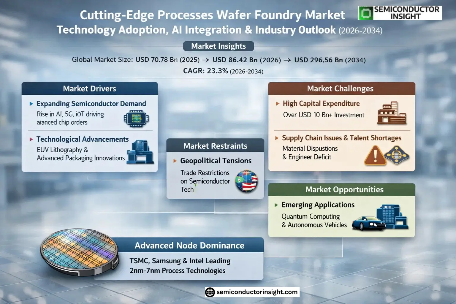
Global Cutting-Edge Processes Wafer Foundry Market size was valued at USD 70.78 billion in 2025. The market is projected to grow from USD 86.42 billion in 2026 to USD 296.56 billion by 2034, exhibiting a CAGR of 23.3% during the forecast period.
Cutting-edge processes wafer foundries specialize in manufacturing semiconductor wafers using advanced process nodes such as 2nm, 3nm, and 5nm technologies, which enable higher transistor density and improved power efficiency for next-generation chips. These foundries play a critical role in producing components for applications like high-performance computing (HPC), smartphones, and AI-driven systems. Currently, only three major players TSMC, Samsung Foundry, and Intel Foundry Services (IFS) dominate this highly specialized market segment due to their technological expertise and massive R&D investments.
The market’s exponential growth is fueled by surging demand for advanced chips across multiple industries, coupled with increasing adoption of AI/ML workloads that require cutting-edge silicon. While geopolitical factors present supply chain challenges, the industry is responding with capacity expansions TSMC alone plans to invest USD 100 billion over three years to meet demand. The transition to smaller nodes continues unabated, with the 3nm segment expected to capture significant market share as leading-edge designs migrate from R&D to volume production.
MARKET DRIVERS
Expanding Semiconductor Demand
Cutting-Edge Processes Wafer Foundry Market is witnessing robust growth due to rising demand for advanced semiconductors in AI, 5G, and IoT applications. Foundries adopting sub-7nm and 3nm processes are seeing increased orders from fabless semiconductor companies. The market is projected to grow at a CAGR of 12% over the next five years.
Technological Advancements
Innovations in extreme ultraviolet (EUV) lithography and advanced packaging techniques are enabling foundries to produce denser, more efficient chips. Leading players are investing over USD 20 billion annually in cutting-edge wafer fabrication processes to maintain competitive advantages.
Government initiatives supporting semiconductor self-sufficiency are further accelerating investments in cutting-edge wafer foundry capabilities across major economies.
MARKET CHALLENGES
High Capital Expenditure Requirements
Establishing and maintaining a cutting-edge wafer foundry requires investments exceeding USD 10 billion, creating significant barriers to entry. The cost of EUV lithography machines alone can reach USD 150 million per unit, limiting participation to only the most capitalized players.
Other Challenges
Supply Chain Vulnerabilities
Disruptions in the semiconductor supply chain, particularly for high-purity silicon and rare earth materials, continue to challenge consistent production in advanced wafer foundry processes.
Talent Shortages
The industry faces a critical shortage of engineers skilled in cutting-edge semiconductor manufacturing processes, with an estimated global deficit of 30,000 qualified professionals.
MARKET RESTRAINTS
Geopolitical Tensions
Trade restrictions and export controls on advanced semiconductor technologies are creating fragmentation in the cutting-edge wafer foundry market. These measures are limiting technology transfers and collaboration between global industry players, potentially slowing innovation cycles.
MARKET OPPORTUNITIES
Emerging Applications
The development of quantum computing, autonomous vehicles, and advanced medical devices is creating new demand for cutting-edge wafer foundry services. These applications require specialized process nodes that only the most advanced foundries can provide, opening premium market segments.
Cutting-Edge Processes Wafer Foundry Market Trends
Advanced Node Dominance in Foundry Landscape
Cutting-Edge Processes Wafer Foundry Market is witnessing rapid evolution with TSMC, Samsung Foundry, and Intel Foundry Services leading 2nm-7nm process technology development. These advanced nodes currently represent over 60% of premium foundry demand, driven by high-performance computing and smartphone applications that require extreme transistor density and power efficiency.
Other Trends
Geographic Capacity Expansion
Major foundries are strategically establishing new facilities outside traditional hubs, with significant investments in US and European locations to strengthen supply chain resilience. This geographic diversification responds to increasing regional demand and mitigates geopolitical risks in semiconductor manufacturing.
Application-Specific Process Optimization
Foundries are developing specialized process variants tailored for HPC, AI accelerators, and automotive applications, moving beyond one-size-fits-all solutions. This trend is creating differentiated offerings that command premium pricing while addressing specific performance, power, and reliability requirements of end markets.
Materials Innovation Driving Performance
The industry is transitioning to novel materials like gate-all-around (GAA) transistors and backside power delivery networks at 2nm nodes. These innovations are critical for maintaining Moore’s Law scaling while addressing fundamental physical limitations of FinFET architectures at advanced nodes.
Ecosystem Collaboration Intensifies
Leading foundries are deepening partnerships with EDA tool providers and IP vendors to accelerate design cycles for cutting-edge nodes. This ecosystem alignment is becoming essential as design complexity reaches unprecedented levels, with full-flow co-optimization now mandatory for successful tapeouts.
COMPETITIVE LANDSCAPE
Key Industry Players
Triangle of Power Dominates Advanced Node Wafer Fabrication
TSMC, Samsung Foundry, and Intel Foundry Services (IFS) currently form the exclusive club capable of manufacturing cutting-edge process wafers below 7nm, collectively controlling over 90% of the advanced node market. TSMC maintains clear leadership with 54% revenue share in 2025, driven by its first-to-market 3nm production and commanding position in 5nm capacity allocation. The competitive dynamics intensified when Intel re-entered the foundry business through IFS, leveraging its IDM 2.0 strategy to challenge the established duopoly.
Beyond the big three, GlobalFoundries and UMC maintain niche positions in trailing-edge nodes while strategically investing in specialty technologies. Emerging Chinese players like SMIC and Hua Hong Semiconductor are accelerating their advanced node roadmaps with government support, though remain constrained by export controls. Specialized foundries including Tower Semiconductor and Vanguard International Semiconductor play vital roles in analog/mixed-signal segments complementary to leading-edge logic.
List of Key Cutting-Edge Processes Wafer Foundry Companies Profiled
- Taiwan Semiconductor Manufacturing Company (TSMC)
- Samsung Foundry
- Intel Foundry Services (IFS)
- GlobalFoundries
- United Microelectronics Corporation (UMC)
- Semiconductor Manufacturing International Corporation (SMIC)
- Hua Hong Semiconductor
- Tower Semiconductor
- Vanguard International Semiconductor (VIS)
- Powerchip Semiconductor Manufacturing (PSMC)
- DB HiTek
- MagnaChip Semiconductor
- Shanghai Huali Microelectronics (HLMC)
- X-FAB Silicon Foundries
- SilTerra Malaysia
Segment Analysis:
| Segment Category | Sub-Segments | Key Insights |
| By Type |
|
3nm Process Segment is currently dominating due to:
|
| By Application |
|
Smartphone Application drives maximum demand due to:
|
| By End User |
|
Fabless Semiconductor Companies are primary users because:
|
| By Technology Node |
|
Gate-All-Around (GAA) Technology is gaining traction due to:
|
| By Foundry Capability |
|
Pure-play Foundries maintain leadership position because:
|
Regional Analysis: Cutting-Edge Processes Wafer Foundry Market
Asia-Pacific foundries lead in gate-all-around transistors and backside power delivery networks, critical for cutting-edge processes. TSMC’s pathfinding initiatives consistently set industry standards adopted globally.
Regional foundries are integrating AI-driven process control systems for yield optimization. Samsung’s AI-powered defect detection and TSMC’s virtual metrology systems represent industry benchmarks in smart manufacturing.
Multi-billion dollar expansions in Taiwan, South Korea and Singapore focus on cutting-edge nodes. Japan’s revived foundry ecosystem attracts investment for specialized processes like image sensors and power devices.
Joint development with material science institutes and equipment vendors accelerates novel process integration. Public-private partnerships drive innovation in advanced packaging like 3D-IC and chiplets.
North America
While trailing Asia in volume production, North America maintains strong cutting-edge process capabilities through Intel Foundry Services and GlobalFoundries’ specialized nodes. The region leads in research collaborations with university nanofabs and DOD-sponsored programs for secure chips. Arizona’s growing foundry cluster benefits from TSMC’s USD 40 billion investment and Intel’s Ohio expansion, focusing on heterogeneous integration technologies. North American strength lies in design-technology co-optimization for AI/ML accelerators and defense applications requiring trusted foundry services.
Europe
Europe’s cutting-edge foundry landscape centers on STMicroelectronics and GlobalFoundries Dresden for FD-SOI and specialty processes. The European Chips Act drives investment in 2nm-capable fabs with focus on automotive and industrial applications. Imec in Belgium serves as global hub for advanced process R&D, particularly in novel materials and beyond-silicon technologies. European foundries differentiate through ultra-low-power processes and MEMS integration for IoT edge devices.
Middle East
The Middle East is emerging through strategic investments in semiconductor manufacturing, with Israel’s Tower Semiconductor leading analog/mixed-signal foundry services. UAE’s ambitious semiconductor strategy includes partnerships for advanced packaging and testing facilities. Regional strengths lie in RF-SOI and power management IC processes, supported by growing demand from 5G and renewable energy sectors.
South America
South America’s role in cutting-edge wafer foundry remains limited but shows potential through specialized analog and MEMS fabs in Brazil. The region benefits from proximity to North American markets for automotive and industrial chips. Growing government incentives aim to develop local semiconductor ecosystems, particularly for power electronics serving renewable energy infrastructure projects.
Report Scope
This market research report provides a comprehensive analysis of the Cutting-Edge Processes Wafer Foundry Market, covering the forecast period 2025–2034. It offers detailed insights into market dynamics, technological advancements, competitive landscape, and key trends shaping the industry.
Key focus areas of the report include:
- Market Overview: The report begins with an overview outlining its current market scenario, key growth indicators, and industry transformation drivers. It discusses macroeconomic factors, demand–supply balance, regulatory landscape, and the strategic role of semiconductors in powering advancements across industries such as automotive, telecommunications, consumer electronics, and industrial automation.
- Market Size & Forecast: Historical data and future projections for revenue, unit shipments, and market value across major regions and segments.
- Segmentation Analysis: Detailed breakdown by product type, technology, application, and end-user industry to identify high-growth segments and investment opportunities.
- Regional Insights: Insights into market performance across North America, Europe, Asia-Pacific, Latin America, and the Middle East & Africa, including country-level analysis where relevant.
- Competitive Landscape: Profiles of leading market participants, including their product offerings, R&D focus, manufacturing capacity, pricing strategies, and recent developments such as mergers, acquisitions, and partnerships.
- Technology Trends & Innovation: Assessment of emerging technologies, integration of AI/IoT, semiconductor design trends, fabrication techniques, and evolving industry standards.
- Market Drivers & Restraints: Evaluation of factors driving market growth along with challenges, supply chain constraints, regulatory issues, and market-entry barriers.
- Stakeholder Insights: Insights for component suppliers, OEMs, system integrators, investors, and policymakers regarding the evolving ecosystem and strategic opportunities.
Primary and secondary research methods are employed, including interviews with industry experts, data from verified sources, and real-time market intelligence to ensure the accuracy and reliability of the insights presented.
FREQUENTLY ASKED QUESTIONS:
What is the current market size of Cutting-Edge Processes Wafer Foundry Market?
-> Cutting-Edge Processes Wafer Foundry Market size was valued at USD 70.78 billion in 2025. The market is projected to grow from USD 86.42 billion in 2026 to USD 296.56 billion by 2034, exhibiting a CAGR of 23.3% during the forecast period.
Which key companies operate in Cutting-Edge Processes Wafer Foundry Market?
-> Key players include TSMC, Samsung Foundry, and Intel Foundry Services (IFS), which currently dominate the market with advanced process nodes like 2nm, 3nm, and 5nm.
What are the key growth drivers?
-> Key growth drivers include increasing demand for high-performance computing (HPC), smartphone innovations, and advancements in semiconductor fabrication technologies.
Which region dominates the market?
-> Asia-Pacific is the fastest-growing region, with significant contributions from China, Japan, and South Korea, while North America remains a key player due to technological leadership.
What are the emerging trends?
-> Emerging trends include adoption of 3nm and 2nm process nodes, integration of AI in semiconductor manufacturing, and expansion of foundry capacities globally.
Get Sample Report PDF for Exclusive Insights
Report Sample Includes
- Table of Contents
- List of Tables & Figures
- Charts, Research Methodology, and more...