Key Statistics
Key Takeaways
- Colloidal ceria slurry accounts for more than 60% of the source market because controlled particle distribution and dispersion stability support lower defectivity and more repeatable planarization than broader calcined-particle formulations in advanced semiconductor processes.
- STI and ILD CMP are the dominant applications because ceria has strong chemical affinity with oxide and can be formulated for high oxide removal while controlling selectivity to nitride, polysilicon and other stop layers.
- Asia Pacific represents more than 60% of global production and consumption, reflecting the concentration of wafer fabrication in Taiwan, South Korea, Japan and China, while the United States remains a major production and formulation base.
- Supplier concentration is high. The source analysis places more than 85% of market share with the five largest producers, making qualification, batch consistency, particle quality and local supply assurance important purchasing factors for semiconductor fabs.
- Advanced packaging creates an additional opportunity. New 2.5D, 3D and hybrid-bonding processes introduce planarization requirements that can extend ceria use beyond traditional front-end STI and ILD polishing.
Ceria CMP Slurry Market Overview
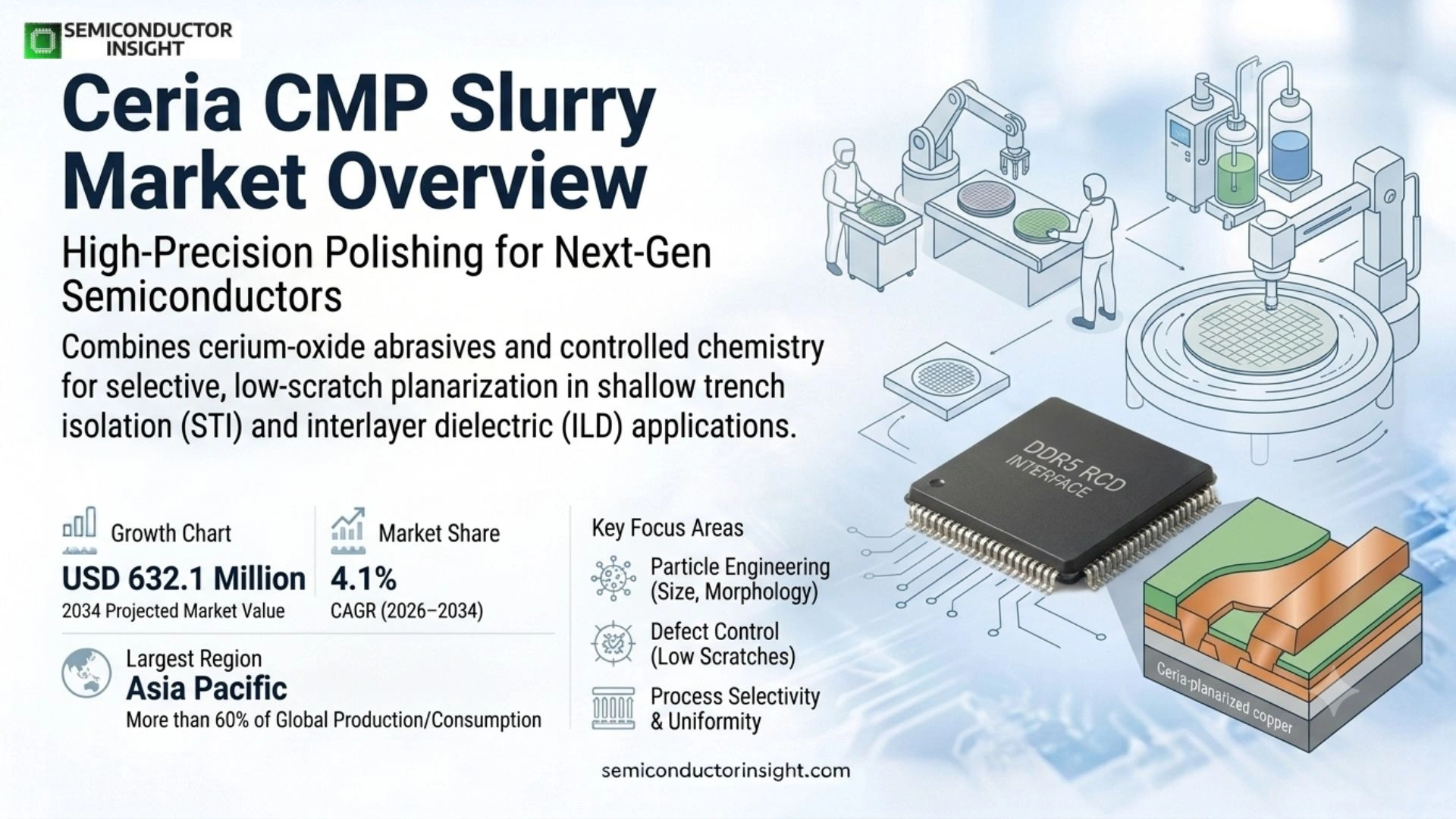
Ceria CMP Slurry market was valued at USD 439.4 million in 2025 and is projected to reach USD 632.1 million by 2034, representing a 4.1% CAGR during 2026–2034. The 2026 estimated market size is USD 457.5 million. Asia Pacific is the largest region, accounting for more than 60% of global production and consumption in the source market structure.
Ceria chemical-mechanical planarization slurry combines cerium-oxide abrasive particles with controlled chemistry to remove and level dielectric or other films during semiconductor manufacturing. Mechanical abrasion and surface chemistry act together, allowing the wafer to be flattened without relying only on high downforce. Ceria is especially valuable in oxide-rich applications such as shallow trench isolation and interlayer dielectrics, where selectivity, low scratch rates and within-wafer uniformity directly affect yield.
Particle engineering separates semiconductor-grade slurry from general-purpose polishing material. Suppliers tune ceria particle size, morphology, surface charge, dispersion stability and additives to balance removal rate with defect control. Smaller and more uniform particles can reduce scratches, but the complete formulation must also control selectivity and remain compatible with post-CMP cleaning. A slurry is therefore qualified as part of a process module together with pad, pressure, chemistry and endpoint conditions.
Demand follows wafer starts, device complexity and the number of CMP steps per wafer. Advanced logic, 3D NAND, DRAM and HBM structures introduce repeated topography-control requirements and narrower defect budgets. New packaging architectures add another layer of opportunity because hybrid bonding, interposers and dense redistribution require extremely flat surfaces. These trends favor process-specific colloidal formulations and application engineering rather than simple growth in bulk abrasive tonnage.
Segment Analysis: By Type
By product type, the report segments the market into Calcined Ceria Slurry and Colloidal Ceria Slurry. Colloidal ceria holds the larger share because advanced devices reward narrow particle-size distribution, stable suspension and lower defectivity, while calcined products remain relevant where mature process economics and removal-rate requirements tolerate a broader particle profile.
| Product type | Material and process characteristics | Market position |
|---|---|---|
| Calcined Ceria Slurry | Calcined ceria is produced through thermal processing that forms crystalline abrasive particles with a broader morphology and size distribution. Formulations can be adjusted through particle classification and additives to control oxide removal and stopping behavior against nitride or polysilicon. The material is proven in established CMP flows where aggressive removal and stable tool recipes are important. | A mature segment serving established semiconductor processes. It remains useful when removal efficiency and proven cost structure outweigh the need for the tightest defect control, but advanced nodes increasingly favor smaller and more uniform colloidal particles as scratch and non-uniformity budgets narrow. |
| Colloidal Ceria Slurry | Colloidal formulations use finer, more uniformly dispersed ceria particles whose surface chemistry can be engineered for stable suspension and controlled oxide interaction. The approach supports low scratch performance, tunable selectivity and tight within-wafer control, but requires sophisticated synthesis, filtration and contamination management. | Largest type, above 60% of the source market. Advanced logic and memory processes favor colloidal systems where rare large particles or unstable agglomerates can destroy valuable die. Once a formulation is qualified with a fab process, switching costs are high because yield must be revalidated across slurry, pad and cleaner interactions. |
Particle size and end-use segmentation
The report also divides demand by particle size and end-use industry. Fine particles below 100 nm are most aligned with advanced-node defect control, while medium and coarse particles retain roles in less sensitive or more aggressive polishing processes. Semiconductor manufacturing is the largest end-use industry, followed by memory, optoelectronics and other polishing applications. Commercial performance depends on the combination of particle size, chemical additives and process integration rather than on abrasive diameter alone.
| Axis | Segments | Commercial implication |
|---|---|---|
| By Particle Size | Fine particles (<100 nm) · Medium particles (100–500 nm) · Coarse particles (>500 nm) | Fine particles are most aligned with advanced-node defect control and high-quality oxide planarization, while larger particles can support stronger mechanical removal in less sensitive processes. Suppliers must balance size with dispersion stability, chemistry and post-CMP cleanability. |
| By End-Use Industry | Semiconductors · Optoelectronics · Memory Devices · Others | Semiconductor wafer fabrication creates the largest and most demanding requirement because CMP is repeated across multilayer structures. Memory adds strong consumption through DRAM and 3D NAND, while optoelectronic and specialty polishing create smaller niches. |
Segment Analysis: By Application
By application, STI/ILD CMP is the dominant segment and the report groups other polishing uses under an additional category. STI and ILD are particularly suitable for ceria because the abrasive chemistry can deliver high oxide removal while additives control selectivity to silicon nitride, polysilicon and other stop layers. Advanced packaging is an emerging strategic extension beyond the primary front-end segmentation.
| Application | Demand characteristics |
|---|---|
| STI/ILD CMP | Shallow trench isolation and interlayer dielectric polishing remove oxide until the surface is sufficiently planar for subsequent lithography and deposition. Ceria’s chemical interaction with silica can deliver efficient oxide removal while additives control stopping behavior on nitride or other films. As patterns become denser, repeatable selectivity and low defectivity become more valuable than maximum polishing speed. |
| Other Semiconductor CMP | Ceria formulations can be adapted to specialty oxide, polysilicon, selected metals, resin and other surfaces when the process benefits from the abrasive’s surface chemistry. These opportunities broaden demand beyond STI and ILD but require separate customer qualifications because material stacks, pads, cleaners and endpoint requirements differ substantially across process modules. |
| Advanced Packaging / 3D Integration | Although not a separate primary application line on the source report, advanced packaging is strategically important because 2.5D, 3D and hybrid-bonding flows introduce new planarization steps. Wafer-to-wafer and die-to-wafer interfaces require very flat surfaces with low defectivity, creating opportunities for ceria formulations adapted to package-level oxide and mixed-material processes. |
Regional Analysis
Asia Pacific dominates the Ceria CMP Slurry market with more than 60% of global production and consumption. Taiwan, South Korea, Japan and China combine leading logic, memory and foundry capacity with a dense materials-supplier network. North America remains a major production and R&D base, Europe is more specialized, and emerging regions rely heavily on imported qualified slurry.
How does ceria slurry demand differ across semiconductor manufacturing regions?
CMP slurry is consumed where wafers are processed, so demand closely follows fab utilization and technology mix. Asia Pacific has the largest wafer-start base and the strongest concentration of advanced logic and memory investment. North America combines established fabs with new capacity and formulation R&D. Europe has smaller volume but stringent automotive and specialty requirements, while other regions create new opportunities only when front-end wafer processing reaches commercial scale.
| Region | Market position | Growth outlook | Demand profile | What decides supplier selection |
|---|---|---|---|---|
| Asia Pacific | >60% of production/consumption | High | Foundry, memory & materials | Yield, local supply and advanced-node qualification |
| North America | Major production base | High | Logic, memory & new fabs | Qualification, local supply and consistency |
| Europe | Specialized | Moderate | Automotive, power & specialty | Reliability, regulatory control and process support |
| South America | Small | Selective | Imported semiconductor materials | Availability and technical support |
| Middle East & Africa | Emerging | Selective | New technology investment | Fab pipeline and reliable imports |
Competitive Landscape
The Ceria CMP Slurry market is highly concentrated. The source analysis places more than 85% of market share with the five largest suppliers and profiles Resonac, Merck, AGC, KC Tech, Anjimirco Shanghai, Soulbrain, Dongjin Semichem, SKC, Saint-Gobain and Ferro. Competitive advantage is built on particle synthesis, formulation chemistry, batch consistency, customer qualification, cleaning compatibility and secure raw-material supply.
AGC differentiates through integrated control from abrasive particle production to finished slurry and emphasizes planarization, material selectivity, uniformity and low defects in STI and ILD processes. Controlling the abrasive as well as the chemistry can reduce raw-particle variability and help formulation teams respond when a fab changes selectivity, removal-rate or defect requirements.
Resonac and other Japanese suppliers have long participated in semiconductor ceria slurry, while Korean companies such as KC Tech, Soulbrain and Dongjin Semichem benefit from proximity to major memory customers. These companies compete through both calcined and colloidal formulations, particle-size tuning, additives and local application engineering rather than through price alone.
Merck, Saint-Gobain and other materials companies contribute purification, chemistry and global customer support. Because a slurry can affect yield across a high-value wafer, fabs often value consistent long-term supply more than a small raw-material saving. Supplier concentration persists when incumbents prove repeatability across many lots and process changes, although customers may qualify second sources to improve resilience.
Competitive tier structure
| Tier | Companies | Basis of competition |
|---|---|---|
| Global leaders | Resonac; AGC; Merck KGaA | Advanced ceria particle technology, global fab qualifications, integrated materials capability and high-purity supply |
| Asian challengers | KC Tech; Soulbrain; Dongjin Semichem; SKC; Anjimirco Shanghai | Local foundry and memory access, competitive cost structures, customization and expanding colloidal portfolios |
| Specialists | Saint-Gobain; Ferro (UWiZ Technology) | Abrasive and specialty slurry capabilities serving selected process and regional niches |
Key companies profiled in the report scope
- Resonac
- Merck KGaA (Versum Materials)
- AGC
- KC Tech
- Anjimirco Shanghai
- Soulbrain
- Dongjin Semichem
- SKC
- Saint-Gobain
- Ferro (UWiZ Technology)
Ceria CMP Slurry Production Capacity & Supply-Side Analysis
Commercial capacity depends on more than blending volume. Semiconductor slurry requires high-purity ceria synthesis, particle-size control, dispersion, chemical formulation, filtration, clean packaging and rigorous lot release. A plant may have physical mixing capacity but still lack qualified output for an advanced fab if particle defects, metal contamination or batch variation exceed process limits. Vertical integration and regional production therefore have direct strategic value.
Leading suppliers emphasize control from abrasive particle through finished slurry because particle morphology and impurity levels determine the ceiling on process performance. Calcined and colloidal routes require different synthesis and classification capability, while additives and filtration create the final process behavior. Capacity should therefore be measured as qualified formulation output rather than tank volume, with analytical capability and batch release acting as practical bottlenecks.
Regional fab expansion creates pressure for local inventory because slurry is a recurring consumable and fabs resist supply interruptions. Suppliers that place blending, warehousing or technical support close to Taiwan, Korea, Japan, China and the United States can reduce lead time and support qualification. Every new site must reproduce the same particle and chemical quality as the original plant, so quality systems and raw-material control remain essential.
Market Dynamics
Growth is supported by higher wafer starts, advanced-node migration, 3D NAND and HBM investment, tighter defect specifications and new advanced-packaging planarization steps. Restraints include customer qualification, rare-earth supply risk, supplier concentration and the difficulty of balancing removal rate with defectivity. Opportunities center on fine-particle colloidal ceria, packaging CMP, post-CMP cleaner integration and localized supply.
MARKET DRIVERS
Drivers Impact Analysis*
| Factor | Forecast impact* | Geographic relevance | Impact timeline |
|---|---|---|---|
| Advanced logic and memory investment | High | Asia Pacific, North America | Medium to long term |
| More CMP steps per complex device | High | Leading-edge fabs | Persistent |
| HBM and 3D NAND scaling | Medium to high | Korea, Taiwan, China, U.S. | Medium term |
| Advanced packaging planarization | Medium | Global packaging hubs | Medium to long term |
*Directional analytical rating; it is not a measured contribution to the headline CAGR.
Advanced device structures require more planarization control
Gate-all-around transistors, 3D NAND and high-density memory introduce vertical structures and repeated material transitions that increase the importance of flat surfaces. As topography becomes more complex, slurry must deliver controlled removal and low defectivity across narrow process windows, supporting premium formulations and stronger application engineering.
Wafer-fab investment expands the recurring consumables base
Every new wafer line creates continuing demand for slurry once it reaches volume production. The commercial effect is recurring rather than one-time: CMP consumables are used on every qualifying wafer, so fab utilization and process-step count matter more to slurry revenue than the initial capital-equipment purchase.
Fine-particle colloidal formulations improve the process window
Colloidal ceria’s leading share reflects advantages in particle uniformity, suspension stability and scratch control. A rare large particle or unstable agglomerate can create a defect that destroys valuable die, so fabs pay for controlled particle populations, filtration and chemistry that maintain selectivity without introducing difficult residue.
Advanced packaging creates an additional planarization frontier
2.5D, 3D and hybrid-bonding processes use interposers, redistribution and mixed materials that can require extremely flat surfaces. Ceria suppliers can grow beyond the front-end STI and ILD base by adapting formulations to package-level oxide or mixed-material CMP while demonstrating low contamination and compatibility with downstream bonding.
MARKET RESTRAINTS
Restraints Impact Analysis*
| Factor | Forecast impact* | Geographic relevance | Impact timeline |
|---|---|---|---|
| Long fab qualification cycles | High | Global | Persistent |
| Batch consistency and defect risk | High | Advanced-node fabs | Persistent |
| Rare-earth and chemical supply concentration | Medium to high | Global supply chain | Persistent |
| Alternative slurry chemistries | Medium | Process-specific | Medium term |
*Directional analytical rating; it is not a measured contribution to the headline CAGR.
Changing slurry is costly for a production fab
A CMP formulation is validated with the pad, tool settings, wafer pattern, cleaner and downstream yield checks. Even when a competitor offers lower price, changing chemistry can alter removal rate, dishing, erosion, scratches or residue. The qualification burden makes incumbent positions sticky but also slows adoption of new products because samples must pass extensive wafer-level testing.
Defect control imposes strict manufacturing discipline
Semiconductor customers need very low metal contamination, narrow particle distribution and minimal agglomerates. Small batch variation can create scratches or nonuniform polishing across many wafers, making slurry quality a direct yield risk. Suppliers must invest in clean production, filtration, particle analytics and statistical process control, raising fixed costs and entry barriers.
Ceria depends on specialized raw-material supply
Cerium oxide is a rare-earth material whose cost and availability can be influenced by upstream processing concentration and geopolitical conditions. Vertical integration reduces exposure but does not eliminate the need for high-purity feedstock. Fabs also pressure suppliers for second-source resilience, requiring vendors to show that alternate raw-material routes do not change process behavior.
Other CMP chemistries can substitute in selected steps
Silica, alumina and newer abrasives can be technically preferable for different films or process conditions. Ceria’s advantage is strongest where oxide chemistry and selectivity justify its use. Suppliers must therefore prove lower defects, better selectivity or lower total process cost for each target stack rather than assuming every new CMP step will use ceria.
MARKET OPPORTUNITIES
Expand colloidal ceria below 100 nm
Advanced fabs need smaller and more uniform abrasive particles as defect budgets tighten. Suppliers that control particle synthesis, surface chemistry and filtration can offer fine-particle formulations tuned for low scratches and stable removal. The commercial opportunity is strongest when a process engineer can verify higher yield or a wider operating window.
Bundle post-CMP cleaning with slurry
Ceria residues can be difficult to remove, creating a natural opportunity for matched cleaning chemistry. A combined slurry-plus-cleaner package can simplify customer troubleshooting, improve defect performance and increase supplier share of process consumables while making the qualification relationship deeper and more difficult for a single-product competitor to displace.
Develop ceria for 3D and advanced packaging
Hybrid bonding and advanced packaging require extremely flat interfaces across wafers, die and package substrates. Suppliers can create new formulations for resin, oxide and mixed-material surfaces if they demonstrate low contamination, high uniformity and compatibility with package-level process temperatures and materials.
Localize supply near new wafer fabs
The fab footprint is expanding beyond traditional clusters. Critical slurry suppliers can establish regional blending, warehousing or technical support close to new fabs to reduce transport risk and accelerate process support. Local production only creates value if it exactly reproduces qualified quality, so centralized particle technology and analytics remain essential.
Ceria CMP Slurry Supply Chain Analysis
Upstream purity determines the ceiling on semiconductor quality
Ceria slurry starts with high-purity cerium compounds that must be converted into abrasive particles without introducing metals or large contaminants. Feedstock origin and synthesis conditions influence crystallinity, surface charge and morphology. Suppliers controlling upstream processing can reduce variability and respond faster when fabs change selectivity or defect requirements.
Particle synthesis creates the functional abrasive
Calcined and colloidal routes produce different particle-size distributions and surface behavior. The abrasive must remove material effectively without causing scratches or local topography damage. Classification, dispersion and particle-surface engineering determine how much chemical selectivity the formulation can use while remaining stable during storage, transport and tool recirculation.
Formulation converts particles into a process recipe
Additives regulate pH, surface chemistry, selectivity and stopping behavior against nitride, polysilicon or other films. Filtration removes agglomerates before shipment, and clean packaging protects the qualified particle population. Supplier application engineers need polishing and metrology capability so they can reproduce customer problems and optimize the complete CMP module.
Fab yield determines supplier economics
The customer values good die rather than liters of slurry. A product that costs more can be attractive if it reduces defects, improves uniformity or widens the process window. This yield linkage creates premium positions for proven suppliers but also demands extremely consistent manufacturing because one off-spec lot can disrupt a high-value production line.
Recent Developments in the Ceria CMP Slurry Market
SEMI highlights new CMP abrasive requirements from GAA, HBM and 3D NAND
SEMI’s Specialty Abrasives for CMP work identifies advanced transistor structures, HBM and 3D NAND as forces requiring changes in CMP processes and abrasive composition, reinforcing the link between device architecture and higher-value slurry engineering.
AGC describes expanding ceria-slurry demand and 3D packaging potential
AGC’s semiconductor business briefing identifies growing ceria usage as device complexity increases and points to emerging 3D-mounting needs, while emphasizing integrated production from abrasive particle through finished slurry.
SEMI reports record 2025 semiconductor-equipment billings
SEMI reported strong wafer-processing investment supported by advanced logic, memory and AI-related capacity. Concentrated front-end spending in Asia reinforces the geographic center of future CMP consumables demand.
AGC expands CMP process positioning at SEMICON West
AGC announced a product display covering CMP slurry and post-CMP cleaner alongside other semiconductor materials, illustrating the strategic extension from polishing chemistry into adjacent cleaning steps where residue control affects yield.
REPORT SCOPE & SEGMENTATION
| Attribute | Details |
|---|---|
| Study Period | 2020–2034 |
| Base Year | 2025 |
| Estimated Year | 2026 |
| Forecast Period | 2026–2034 |
| Historical Period | 2020–2025 |
| Market Size 2025 | USD 439.4 million |
| Market Size 2034 | USD 632.1 million |
| Growth Rate | CAGR of 4.1% from 2026–2034 |
| Unit | Value (USD Million) and volume (Tons) |
| Segmentation | By Product Type, By Application, By Particle Size, By End-Use Industry, By Region |
| By Product Type | Calcined Ceria Slurry · Colloidal Ceria Slurry |
| By Application | STI/ILD CMP · Others (Filter) |
| By Particle Size | Fine particle slurries (<100nm) · Medium particle slurries (100–500nm) · Coarse particle slurries (>500nm) |
| By End-Use Industry | Semiconductors · Optoelectronics · Memory Devices · Others |
| By Region | Each region analysed by product type, application, particle size, end-use industry and country marketNorth AmericaUnited States, Canada, MexicoEuropeGermany, France, United Kingdom, Italy and other European marketsAsia PacificTaiwan, South Korea, Japan, China, India, Southeast Asia and other Asian marketsSouth AmericaBrazil, Argentina and other South American marketsMiddle East & AfricaIsrael, UAE, Saudi Arabia, South Africa and other MEA markets |
| Key Companies Profiled | Resonac · Merck KGaA (Versum Materials) · AGC · KC Tech · Anjimirco Shanghai · Soulbrain · Dongjin Semichem · SKC · Saint-Gobain · Ferro (UWiZ Technology) |
| Customization Scope | Free report customization equivalent to up to four analyst working days with purchase. Addition or alteration to country, regional and segment scope. |
Frequently Asked Questions
What is the 2025 size of the Ceria CMP Slurry market?
The normalized market size is USD 439.4 million in 2025 and is projected to reach USD 632.1 million by 2034. The 2026 estimate is USD 457.5 million and the 2026–2034 CAGR is 4.1%. The series is derived from the published USD 422 million 2024 and USD 583 million 2032 market-size anchors.
Which product type leads the market?
Colloidal ceria slurry leads the product mix and represents more than 60% of the source market. Its advantage comes from tighter particle-size distribution, stable dispersion and lower defectivity, which align with advanced semiconductor processes. Calcined ceria remains important where removal rate and mature process economics favor a broader abrasive profile.
Which application dominates ceria slurry demand?
STI and ILD CMP dominate demand because ceria is effective for planarizing oxide while additives can control selectivity against silicon nitride, polysilicon and other stop layers. These process steps recur across multilayer logic and memory devices, creating consistent high-volume consumption in leading wafer fabs.
Which region leads in 2025?
Asia Pacific is the largest region with more than 60% of global production and consumption in the source analysis. Taiwan, South Korea, Japan and China combine high wafer-start volumes with major foundry, memory and materials suppliers, while the United States remains an important production and R&D base.
What is the estimated 2026 market size?
The estimated 2026 market size is USD 457.5 million. This value follows the constant annual growth factor implied by the published 2024 and 2032 market-size anchors and is used consistently in the Key Statistics, Market Overview, Report Scope and FAQ sections.
What are the main growth drivers?
The main drivers are advanced logic and memory investment, more CMP steps per complex device, growth in HBM and 3D NAND, tighter defect specifications and the emergence of advanced-packaging planarization. Thd:#f7f9fb;padding:12px;text-align:left”>Geographic relevanceImpact timelineAdvanced logic and memory investmentHighAsia Pacific, North AmericaMedium to long termMore CMP steps per complex deviceHighLeading-edge fabsPersistentHBM and 3D NAND scalingMedium to highKorea, Taiwan, China, U.S.Medium termAdvanced packaging planarizationMediumGlobal packaging hubsMedium to long term
*Directional analytical rating; it is not a measured contribution to the headline CAGR.
Advanced device structures require more planarization control
Gate-all-around transistors, 3D NAND and high-density memory introduce vertical structures and repeated material transitions that increase the importance of flat surfaces. As topography becomes more complex, slurry must deliver controlled removal and low defectivity across narrow process windows, supporting premium formulations and stronger application engineering.
Wafer-fab investment expands the recurring consumables base
Every new wafer line creates continuing demand for slurry once it reaches volume production. The commercial effect is recurring rather than one-time: CMP consumables are used on every qualifying wafer, so fab utilization and process-step count matter more to slurry revenue than the initial capital-equipment purchase.
Fine-particle colloidal formulations improve the process window
Colloidal ceria’s leading share reflects advantages in particle uniformity, suspension stability and scratch control. A rare large particle or unstable agglomerate can create a defect that destroys valuable die, so fabs pay for controlled particle populations, filtration and chemistry that maintain selectivity without introducing difficult residue.
Advanced packaging creates an additional planarization frontier
2.5D, 3D and hybrid-bonding processes use interposers, redistribution and mixed materials that can require extremely flat surfaces. Ceria suppliers can grow beyond the front-end STI and ILD base by adapting formulations to package-level oxide or mixed-material CMP while demonstrating low contamination and compatibility with downstream bonding.
MARKET RESTRAINTS
Restraints Impact Analysis*
| Factor | Forecast impact* | Geographic relevance | Impact timeline |
|---|---|---|---|
| Long fab qualification cycles | High | Global | Persistent |
| Batch consistency and defect risk | High | Advanced-node fabs | Persistent |
| Rare-earth and chemical supply concentration | Medium to high | Global supply chain | Persistent |
| Alternative slurry chemistries | Medium | Process-specific | Medium term |
*Directional analytical rating; it is not a measured contribution to the headline CAGR.
Changing slurry is costly for a production fab
A CMP formulation is validated with the pad, tool settings, wafer pattern, cleaner and downstream yield checks. Even when a competitor offers lower price, changing chemistry can alter removal rate, dishing, erosion, scratches or residue. The qualification burden makes incumbent positions sticky but also slows adoption of new products because samples must pass extensive wafer-level testing.
Defect control imposes strict manufacturing discipline
Semiconductor customers need very low metal contamination, narrow particle distribution and minimal agglomerates. Small batch variation can create scratches or nonuniform polishing across many wafers, making slurry quality a direct yield risk. Suppliers must invest in clean production, filtration, particle analytics and statistical process control, raising fixed costs and entry barriers.
Ceria depends on specialized raw-material supply
Cerium oxide is a rare-earth material whose cost and availability can be influenced by upstream processing concentration and geopolitical conditions. Vertical integration reduces exposure but does not eliminate the need for high-purity feedstock. Fabs also pressure suppliers for second-source resilience, requiring vendors to show that alternate raw-material routes do not change process behavior.
Other CMP chemistries can substitute in selected steps
Silica, alumina and newer abrasives can be technically preferable for different films or process conditions. Ceria’s advantage is strongest where oxide chemistry and selectivity justify its use. Suppliers must therefore prove lower defects, better selectivity or lower total process cost for each target stack rather than assuming every new CMP step will use ceria.
MARKET OPPORTUNITIES
Expand colloidal ceria below 100 nm
Advanced fabs need smaller and more uniform abrasive particles as defect budgets tighten. Suppliers that control particle synthesis, surface chemistry and filtration can offer fine-particle formulations tuned for low scratches and stable removal. The commercial opportunity is strongest when a process engineer can verify higher yield or a wider operating window.
Bundle post-CMP cleaning with slurry
Ceria residues can be difficult to remove, creating a natural opportunity for matched cleaning chemistry. A combined slurry-plus-cleaner package can simplify customer troubleshooting, improve defect performance and increase supplier share of process consumables while making the qualification relationship deeper and more difficult for a single-product competitor to displace.
Develop ceria for 3D and advanced packaging
Hybrid bonding and advanced packaging require extremely flat interfaces across wafers, die and package substrates. Suppliers can create new formulations for resin, oxide and mixed-material surfaces if they demonstrate low contamination, high uniformity and compatibility with package-level process temperatures and materials.
Localize supply near new wafer fabs
The fab footprint is expanding beyond traditional clusters. Critical slurry suppliers can establish regional blending, warehousing or technical support close to new fabs to reduce transport risk and accelerate process support. Local production only creates value if it exactly reproduces qualified quality, so centralized particle technology and analytics remain essential.
Ceria CMP Slurry Supply Chain Analysis
Upstream purity determines the ceiling on semiconductor quality
Ceria slurry starts with high-purity cerium compounds that must be converted into abrasive particles without introducing metals or large contaminants. Feedstock origin and synthesis conditions influence crystallinity, surface charge and morphology. Suppliers controlling upstream processing can reduce variability and respond faster when fabs change selectivity or defect requirements.
Particle synthesis creates the functional abrasive
Calcined and colloidal routes produce different particle-size distributions and surface behavior. The abrasive must remove material effectively without causing scratches or local topography damage. Classification, dispersion and particle-surface engineering determine how much chemical selectivity the formulation can use while remaining stable during storage, transport and tool recirculation.
Formulation converts particles into a process recipe
Additives regulate pH, surface chemistry, selectivity and stopping behavior against nitride, polysilicon or other films. Filtration removes agglomerates before shipment, and clean packaging protects the qualified particle population. Supplier application engineers need polishing and metrology capability so they can reproduce customer problems and optimize the complete CMP module.
Fab yield determines supplier economics
The customer values good die rather than liters of slurry. A product that costs more can be attractive if it reduces defects, improves uniformity or widens the process window. This yield linkage creates premium positions for proven suppliers but also demands extremely consistent manufacturing because one off-spec lot can disrupt a high-value production line.
Recent Developments in the Ceria CMP Slurry Market
SEMI highlights new CMP abrasive requirements from GAA, HBM and 3D NAND
SEMI’s Specialty Abrasives for CMP work identifies advanced transistor structures, HBM and 3D NAND as forces requiring changes in CMP processes and abrasive composition, reinforcing the link between device architecture and higher-value slurry engineering.
AGC describes expanding ceria-slurry demand and 3D packaging potential
AGC’s semiconductor business briefing identifies growing ceria usage as device complexity increases and points to emerging 3D-mounting needs, while emphasizing integrated production from abrasive particle through finished slurry.
SEMI reports record 2025 semiconductor-equipment billings
SEMI reported strong wafer-processing investment supported by advanced logic, memory and AI-related capacity. Concentrated front-end spending in Asia reinforces the geographic center of future CMP consumables demand.
AGC expands CMP process positioning at SEMICON West
AGC announced a product display covering CMP slurry and post-CMP cleaner alongside other semiconductor materials, illustrating the strategic extension from polishing chemistry into adjacent cleaning steps where residue control affects yield.
REPORT SCOPE & SEGMENTATION
| Attribute | Details |
|---|---|
| Study Period | 2020–2034 |
| Base Year | 2025 |
| Estimated Year | 2026 |
| Forecast Period | 2026–2034 |
| Historical Period | 2020–2025 |
| Market Size 2025 | USD 439.4 million |
| Market Size 2034 | USD 632.1 million |
| Growth Rate | CAGR of 4.1% from 2026–2034 |
| Unit | Value (USD Million) and volume (Tons) |
| Segmentation | By Product Type, By Application, By Particle Size, By End-Use Industry, By Region |
| By Product Type | Calcined Ceria Slurry · Colloidal Ceria Slurry |
| By Application | STI/ILD CMP · Others (Filter) |
| By Particle Size | Fine particle slurries (<100nm) · Medium particle slurries (100–500nm) · Coarse particle slurries (>500nm) |
| By End-Use Industry | Semiconductors · Optoelectronics · Memory Devices · Others |
| By Region | Each region analysed by product type, application, particle size, end-use industry and country marketNorth AmericaUnited States, Canada, MexicoEuropeGermany, France, United Kingdom, Italy and other European marketsAsia PacificTaiwan, South Korea, Japan, China, India, Southeast Asia and other Asian marketsSouth AmericaBrazil, Argentina and other South American marketsMiddle East & AfricaIsrael, UAE, Saudi Arabia, South Africa and other MEA markets |
| Key Companies Profiled | Resonac · Merck KGaA (Versum Materials) · AGC · KC Tech · Anjimirco Shanghai · Soulbrain · Dongjin Semichem · SKC · Saint-Gobain · Ferro (UWiZ Technology) |
| Customization Scope | Free report customization equivalent to up to four analyst working days with purchase. Addition or alteration to country, regional and segment scope. |
Frequently Asked Questions
What is the 2025 size of the Ceria CMP Slurry market?
The normalized market size is USD 439.4 million in 2025 and is projected to reach USD 632.1 million by 2034. The 2026 estimate is USD 457.5 million and the 2026–2034 CAGR is 4.1%. The series is derived from the published USD 422 million 2024 and USD 583 million 2032 market-size anchors.
Which product type leads the market?
Colloidal ceria slurry leads the product mix and represents more than 60% of the source market. Its advantage comes from tighter particle-size distribution, stable dispersion and lower defectivity, which align with advanced semiconductor processes. Calcined ceria remains important where removal rate and mature process economics favor a broader abrasive profile.
Which application dominates ceria slurry demand?
STI and ILD CMP dominate demand because ceria is effective for planarizing oxide while additives can control selectivity against silicon nitride, polysilicon and other stop layers. These process steps recur across multilayer logic and memory devices, creating consistent high-volume consumption in leading wafer fabs.
Which region leads in 2025?
Asia Pacific is the largest region with more than 60% of global production and consumption in the source analysis. Taiwan, South Korea, Japan and China combine high wafer-start volumes with major foundry, memory and materials suppliers, while the United States remains an important production and R&D base.
What is the estimated 2026 market size?
The estimated 2026 market size is USD 457.5 million. This value follows the constant annual growth factor implied by the published 2024 and 2032 market-size anchors and is used consistently in the Key Statistics, Market Overview, Report Scope and FAQ sections.
What are the main growth drivers?
The main drivers are advanced logic and memory investment, more CMP steps per complex device, growth in HBM and 3D NAND, tighter defect specifications and the emergence of advanced-packaging planarization. These factors increase demand for fine-particle formulations and application engineering rather than simple bulk abrasive volume.
What are the main restraints?
The major restraints are long fab qualification cycles, strict lot-to-lot consistency requirements, rare-earth and specialty-chemical supply risk and competition from silica or other slurry chemistries in applications where ceria does not provide the best total process economics. High supplier concentration also creates pressure for qualified second sources.
Why are fine particles important?
Fine particles can reduce scratches and improve within-wafer control when advanced processes have very small defect budgets. Colloidal ceria can be produced with much finer and more uniform particles than conventional calcined material. Final performance still depends on chemical additives, pad behavior, filtration and post-CMP cleaning rather than particle size by itself.
What opportunity does advanced packaging create?
2.5D, 3D and hybrid-integration processes add new surfaces that require extreme flatness before bonding or redistribution. Industry suppliers are developing ceria-related solutions for 3D mounting and package-level CMP, giving the market a path to expand beyond traditional front-end STI and ILD applications.
What does the report cover?
The report covers calcined and colloidal ceria slurry; STI and ILD CMP plus other uses; fine, medium and coarse particle sizes; semiconductor, optoelectronic, memory and other end uses; five global regions; production and supply analysis; and the full supplier list shown in the Report Scope table.
Research Sources & Evidence Base
View primary and authoritative evidence used in this overview
- AGC. CMP Slurry – Ceria slurry for STI/ILD Applications – Official product description covering integrated abrasive-to-slurry manufacturing, STI/ILD use, planarization, selectivity and defect-control requirements.
- AGC. Semiconductor-related Business Briefing – June 2026 official briefing on ceria-slurry positioning, integrated production and emerging 3D-mounting demand.
- KC Tech. Ceria Slurry product portfolio – Official product information detailing calcined and colloidal ceria particle-size ranges and process functions.
- SEMI. CMP Technologies and Markets – Industry overview linking CMP growth to advanced logic, memory, 3D NAND and new materials.
- SEMI. Specialty Abrasives for CMP – Industry evidence on ceria and other abrasives, GAA, HBM, 3D NAND and advanced packaging.
- TSMC. 2025 Annual Report – Primary foundry evidence on leading-edge production migration that increases planarization complexity.
Get Sample Report PDF for Exclusive Insights
Report Sample Includes
- Table of Contents
- List of Tables & Figures
- Charts, Research Methodology, and more...
 Download Sample Report PDF