
Key Statistics
Key Takeaways
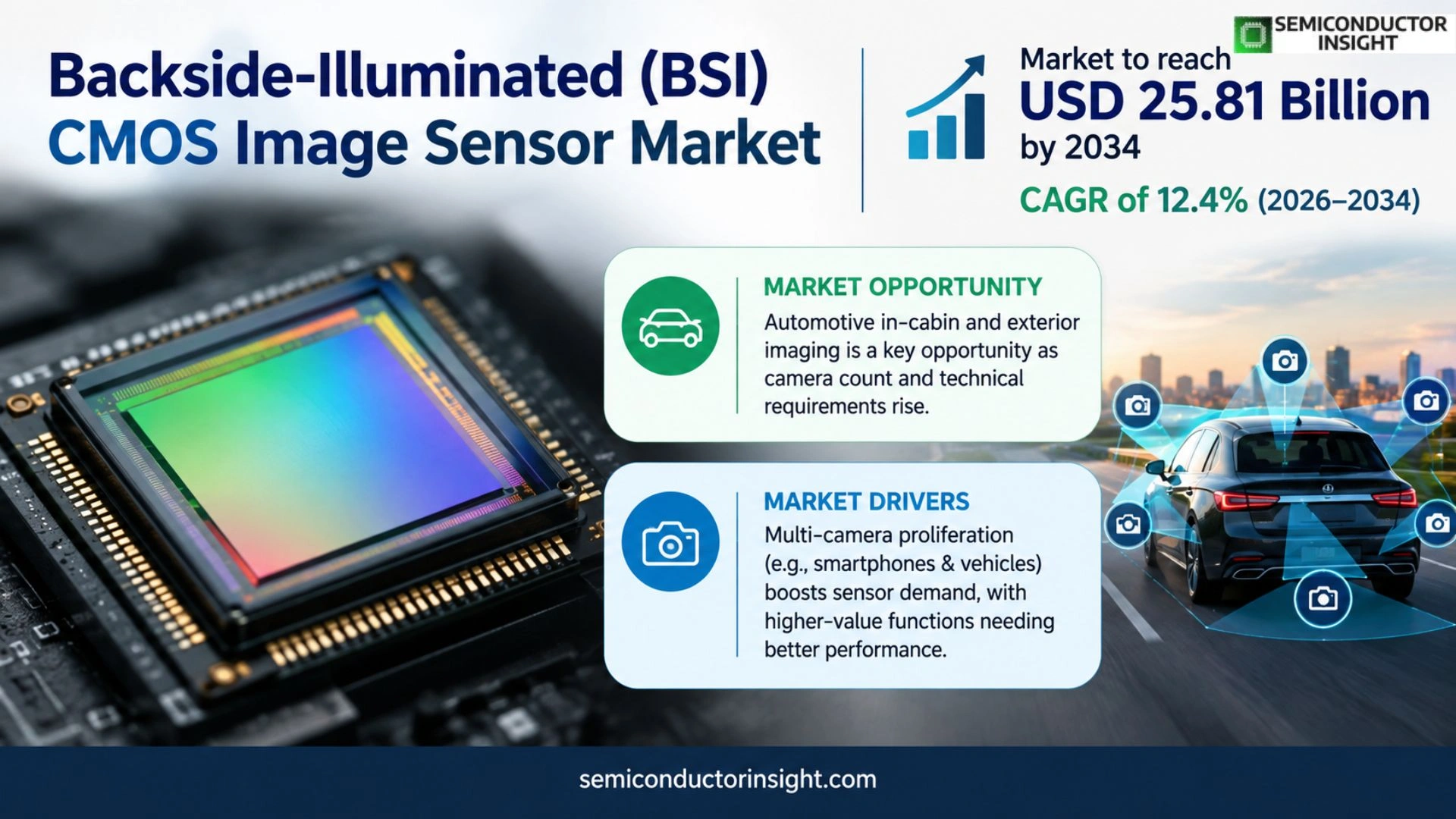
- The validated forecast places the market at USD 8.98 billion in 2025 and USD 25.81 billion by 2034, representing a 12.4% CAGR during 2026–2034. Expansion is supported by increasing camera content, more demanding low-light specifications and a rising mix of stacked sensor architectures.
- More-than-10-megapixel sensors capture the largest value pool because flagship and upper-midrange mobile devices increasingly combine high resolution with on-sensor processing, multi-camera systems and advanced pixel technologies.
- Automotive imaging is among the fastest-growing applications as exterior perception, in-cabin monitoring, electronic mirrors and parking assistance require high dynamic range, near-infrared response and dependable operation across difficult lighting conditions.
- Asia Pacific leads through the combined strength of Japanese and Korean sensor suppliers, Taiwanese foundry and packaging capacity, Chinese device makers and the region’s large consumer-electronics manufacturing base.
- Stacking and global-shutter performance are major competitive differentiators. Separating pixel and logic layers adds processing flexibility, while backside illumination improves photon collection; however, wafer complexity, qualification demands and capital intensity constrain new entrants.
Backside-Illuminated (BSI) CMOS Image Sensor Market Overview
Backside-Illuminated (BSI) CMOS Image Sensor Market was valued at USD 8.98 billion in 2025 and is projected to reach USD 25.81 billion by 2034, growing at a CAGR of 12.4% during 2026–2034. Asia Pacific held the largest regional position in 2025, supported by concentrated manufacturing, downstream electronics production and established component supply networks.
Backside illumination reverses the conventional CMOS image-sensor structure so incoming light reaches the photodiode without first passing through much of the metal interconnect stack. This improves photon collection, particularly as pixel pitches shrink, and enables better low-light performance within compact camera modules. The report segments the market by Less than 5 Megapixels, 5–10 Megapixels and More than 10 Megapixels; Rolling Shutter and Global Shutter; Basic BSI CIS and Stacked BSI CIS; and six application groups spanning consumer, automotive, industrial, medical and security markets.
Commercial differentiation increasingly comes from the full imaging chain rather than quantum efficiency alone. Pixel size, full-well capacity, conversion gain, HDR architecture, readout speed, NIR response, on-chip memory, image-signal processing and interface standards determine whether a sensor fits a smartphone, automotive camera or factory-vision system. Sony’s automotive IMX828 supports high dynamic range and integrated MIPI A-PHY, while ST’s VD55G0 combines a BSI global shutter with a 3D-stacked architecture and high frame rate, illustrating how logic integration is becoming central to product value.
The market is also becoming more application-specific. Mobile suppliers optimize fine pixels, multi-frame HDR and power, automotive suppliers prioritize functional safety, LED flicker mitigation and temperature performance, and machine-vision suppliers emphasize global shutter and deterministic timing. Medical and security systems may require enhanced NIR sensitivity or unusual package formats. This fragmentation favors vendors with reusable pixel platforms and scalable manufacturing because they can adapt a common BSI technology base to many customer programs while preserving qualification and yield economics.
Segment Analysis: By Type
By type, the BSI CMOS Image Sensor market is segmented into Less than 5 Megapixels · 5–10 Megapixels · More than 10 Megapixels. Each category represents a different degree of integration, qualification burden and value capture, so suppliers compete through a combination of material performance, design support, manufacturing consistency, package architecture and application-specific testing rather than through unit price alone.
| Resolution segment | Market interpretation |
|---|---|
| Less than 5 Megapixels | Sub-5-megapixel BSI sensors remain important in driver monitoring, occupancy monitoring, industrial sensing, medical devices, security peripherals and compact embedded vision. These applications often prioritize sensitivity, global shutter, low power or NIR response over extreme spatial resolution. Sony’s approximately 5-megapixel IMX775 and OMNIVISION’s 1.5-megapixel OX01N1B show that lower-resolution devices can still command substantial technical value when paired with automotive qualification, NIR performance or specialized shutter architectures. |
| 5–10 Megapixels | The 5–10-megapixel segment is commercially important in automotive exterior cameras, surveillance, machine vision and selected consumer systems because it balances detailed imaging with manageable data rates and optical requirements. Sony’s 8.34-megapixel IMX828 targets automotive cameras with HDR and MIPI A-PHY, while OMNIVISION’s 8-megapixel OX08D20 addresses exterior automotive vision. Competition therefore centers on dynamic range, safety support, temperature robustness, interface integration and performance under LED lighting as much as raw resolution. |
| More than 10 Megapixels | More-than-10-megapixel BSI sensors lead premium consumer imaging and are expanding into professional, scientific and specialized industrial systems. Sony’s 50-megapixel LYT-828 and approximately 200-megapixel LYTIA 901 demonstrate ongoing mobile resolution scaling, while Canon announced a 410-megapixel full-frame back-illuminated stacked sensor in January 2025 for surveillance, medicine and industry. Higher resolution raises bandwidth, heat and signal-processing requirements, making stacked architecture and high-speed readout increasingly important competitive differentiators. |
Segment Analysis: By Application
By application, the market covers Consumer Electronics · Automotive · Industrial · Medical · Security and Surveillance · Others. Demand varies by production volume and qualification intensity: consumer programmes reward scale and miniaturisation, while automotive, industrial, aerospace, medical or security designs place greater weight on reliability evidence, long product availability and system-level performance under demanding operating conditions.
| Application | Demand characteristics |
|---|---|
| Consumer Electronics | Consumer electronics remain the largest application pool because smartphones, tablets, cameras, laptops and wearables ship at enormous volumes and increasingly use multiple image sensors per device. BSI enables small pixels and compact modules while maintaining low-light sensitivity. Premium smartphones drive rapid transitions toward stacked designs, high dynamic range and very high resolution, but mid-range devices preserve strong demand for cost-optimized BSI sensors where die size, yield and power consumption are more important than the most advanced imaging functions. |
| Automotive | Automotive is one of the fastest-growing applications as vehicles add front, rear, surround-view, driver-monitoring and occupant-monitoring cameras. Suppliers must combine BSI sensitivity with HDR, LED flicker mitigation, NIR performance, functional safety and long temperature-range operation. Sony’s 2025 IMX775 and IMX828 and OMNIVISION’s OX05C demonstrate the competitive emphasis on in-cabin and exterior camera requirements. Qualification cycles are long, giving approved sensors multiyear revenue potential once designed into vehicle platforms. |
| Industrial | Industrial BSI sensors are used in machine vision, barcode readers, robotics, inspection and automation where high frame rates, deterministic timing and low-light sensitivity can improve throughput and defect detection. Global-shutter architectures are particularly important for moving objects because they reduce geometric distortion. ST’s VD55G0 illustrates a compact BSI global-shutter design capable of high frame rates and strong NIR sensitivity, while Sony and other suppliers increasingly combine sensors with edge processing for smarter factory-vision systems. |
| Medical | Medical applications include endoscopy, diagnostic cameras, surgical imaging, ophthalmology, microscopy and compact monitoring equipment. BSI can improve sensitivity in space-constrained optical systems, while specialized packaging and low noise are critical for clinical image quality. Medical qualification can extend product lifecycles and support premium pricing, but suppliers face strict documentation and change-control requirements. High-resolution sensors may enable more detailed imaging, while small-pixel or NIR-optimized devices support miniature probes and fluorescence or low-light applications. |
| Security | Security and surveillance systems use BSI sensors because low-light sensitivity, HDR and NIR performance improve imaging across day/night conditions. High-resolution products expand identification range, while larger-pixel or specialized sensors improve night performance. Canon’s 2025 410-megapixel full-frame sensor demonstrates a premium extreme-resolution path for surveillance and specialized monitoring, while mainstream IP cameras use smaller, lower-cost BSI devices. Market demand therefore spans very different price points but consistently rewards strong low-light and dynamic-range performance. |
| Other | Other applications include drones, scientific imaging, augmented reality, smart infrastructure, biometrics, aerospace and emerging physical-AI systems. These niches can require unusual combinations of resolution, global shutter, frame rate, NIR response or radiation and environmental performance. Sony’s 2026 collaboration with Mitsubishi Electric to develop AI-powered vision sensors for factory automation illustrates how image sensors can evolve into intelligent sensing nodes that combine optical capture with local processing, increasing value beyond the raw pixel array. |
Regional Analysis
Asia Pacific is the largest regional market for BSI CMOS Image Sensor products, combining an established component-production ecosystem with major downstream customers. North America and Europe are strategically important for premium, automotive, aerospace, industrial and specialised applications, while South America and Middle East & Africa are primarily import- and project-led markets where distributor reach, local support and supply continuity shape vendor selection.
How does regional demand differ across this market?
Asia Pacific is the largest BSI CMOS image sensor market because it concentrates the leading supply chain for image sensors, memory, advanced logic, packaging and consumer-electronics manufacturing. Japan hosts Sony and Canon, South Korea hosts Samsung Electronics and SK Hynix, China includes GalaxyCore and SmartSens, and Taiwan provides advanced foundry capacity. North America contributes substantial design demand in smartphones, automotive, security and industrial vision; Europe is strong in automotive and machine vision; South America and Middle East & Africa remain more import-led but benefit from expanding security, mobility and smartphone adoption.
| Region | Position | Commercial logic |
|---|---|---|
| Asia Pacific | Largest | The region combines sensor design, wafer fabrication, advanced packaging, smartphones, cameras and automotive electronics. Sony’s 2026 preliminary TSMC joint-venture plan for next-generation image sensors in Kumamoto underscores continued investment in local production capability and manufacturing resilience. |
| North America | High-value demand market | Smartphone ecosystems, autonomous systems, medical imaging, industrial automation and security create demand for advanced BSI sensors. Supplier success depends on platform qualification, software integration and access to major device and system OEMs rather than local image-sensor fabrication alone. |
| Europe | Automotive and industrial stronghold | European automakers, industrial machinery companies and photonics firms create strong demand for HDR, global-shutter and safety-oriented sensors. STMicroelectronics also provides regional semiconductor capability, particularly for embedded and industrial vision. |
| South America | Emerging import-led market | Demand is tied to smartphones, security cameras, automotive electronics and industrial modernization, with Brazil the largest regional opportunity. Most sensors arrive inside imported modules or finished electronics rather than through a local front-end semiconductor supply chain. |
| Middle East & Africa | Security and infrastructure opportunity | Smart-city, security, mobility and telecom investment create camera demand, while consumer smartphone adoption broadens unit volumes. Most image sensors are imported through device and camera manufacturers, so distribution and OEM platform wins determine regional exposure. |
Key BSI CMOS Image Sensor Manufacturers and Competitive Landscape
The BSI CMOS Image Sensor competitive landscape includes global technology leaders, diversified semiconductor or component groups, RF and imaging specialists, and regional manufacturers. The report profiles every named company across product positioning, manufacturing footprint, application exposure, recent development activity and strategic strengths; the complete coverage list is reproduced below so the intended company universe is explicit.
Competition is led by vertically integrated image-sensor specialists and diversified semiconductor manufacturers. Sony Semiconductor Solutions is the benchmark supplier in premium mobile and increasingly automotive imaging, combining proprietary pixel design with stacked architectures and large manufacturing investments. Samsung competes in high-resolution mobile sensors, OMNIVISION spans mobile, automotive and industrial markets, and STMicroelectronics targets embedded vision and global-shutter applications. GalaxyCore and SmartSens strengthen China’s domestic supply base, while Canon differentiates through specialized high-resolution and professional imaging technology.
The key competitive moat is cumulative pixel and process know-how. Shrinking pixel pitch while preserving quantum efficiency, full-well capacity and crosstalk performance requires advanced optical stacks and semiconductor processes. Stacked BSI adds a second challenge because the pixel wafer and logic wafer must be fabricated, aligned and bonded with high yield. Suppliers that can reuse proven platforms across multiple resolutions reduce development cost, while application-specific HDR, NIR and shutter capabilities help them win designs where generic smartphone sensors cannot satisfy system requirements.
| Competitive group | Companies and positioning |
|---|---|
| Global image-sensor leaders | Sony Semiconductor Solutions, Samsung Electronics, OmniVision Technologies and STMicroelectronics compete through advanced pixel architectures, stacked designs, automotive qualification, global shutter and broad customer access. Their scale supports continuous process investment and multiple application-specific product families. |
| Automotive, industrial and diversified semiconductor suppliers | ON Semiconductor, Panasonic Corporation, Canon Inc., Toshiba Electronic Devices, Himax Technologies, PixArt Imaging and Silicon Optronics participate through automotive, industrial, professional or specialized imaging portfolios. Their strengths are often tied to system relationships, optical expertise or niche sensor architectures rather than total mobile-sensor volume. |
| Asia-based growth and regional suppliers | GalaxyCore Inc., Smartsens Technology, SK Hynix and SOI Semiconductor strengthen regional competition through mobile, automotive, security and specialty image-sensor offerings. They benefit from proximity to Asian electronics manufacturing and can compete through cost, local qualification and product customization. |
Key companies profiled
- Sony Semiconductor Solutions
- Samsung Electronics
- OmniVision Technologies
- STMicroelectronics
- ON Semiconductor
- GalaxyCore Inc.
- Panasonic Corporation
- Smartsens Technology
- Canon Inc.
- SK Hynix
- SOI Semiconductor
- Toshiba Electronic Devices
- Himax Technologies
- PixArt Imaging
- Silicon Optronics
BSI CMOS Image Sensor Production Capacity Analysis
Production capacity is a material competitive factor in the BSI CMOS Image Sensor market because electrical performance depends on specialised processes, qualified materials, repeatable yields and application-specific test capability. Capacity cannot be assessed only by nominal factory floor area: effective supply is the output that passes dimensional, electrical, reliability and customer qualification requirements at the required product mix.
BSI image-sensor capacity is determined by more than nominal wafer starts. Pixel wafers require specialized photodiode, isolation and optical-stack processes, while stacked sensors also require separate logic wafers, wafer bonding, thinning, through-silicon or hybrid interconnect processes, packaging and image-quality test. A supplier can therefore face bottlenecks in bonding or back-end test even when front-end wafer capacity is available. Yield becomes especially important for large die or very high-resolution sensors because defects can destroy more value per wafer.
Sony’s May 2026 preliminary agreement with TSMC provides direct evidence that next-generation image-sensor manufacturing capacity remains a strategic issue. The companies plan to examine development and production lines at a new Sony Semiconductor Manufacturing facility in Koshi, Kumamoto, with possible additional Nagasaki investment. The project is linked to expanding automotive and robotics demand, suggesting that sensor capacity planning is increasingly influenced by physical-AI workloads rather than smartphones alone. Regional diversification also reduces concentration risk in the broader Japanese production network.
BSI CMOS Image Sensor Market Dynamics: Drivers, Restraints and Opportunities
BSI CMOS Image Sensor market growth reflects expanding electronic content and higher performance requirements, moderated by manufacturing complexity, long qualification cycles and competing technologies. The impact ranges below are directional analytical estimates rather than additive forecasts; they show the relative pressure each factor can place on the baseline CAGR when other assumptions remain broadly stable.
The main technology dynamic is migration from basic BSI toward stacked BSI. Separating the pixel layer from the logic layer allows each wafer to use a process optimized for its function and creates room for faster readout, on-chip memory, HDR processing and increasingly AI-related logic. Sony’s high-end mobile sensors and Canon’s 410-megapixel stacked device show how the architecture can support both small-pixel consumer designs and extreme-resolution specialized sensors. Stacking increases manufacturing complexity but expands the performance ceiling.
A second dynamic is convergence between rolling and global shutter use cases. Rolling shutter remains cost-effective and high quality for many mobile and automotive cameras, while global shutter is moving into applications that historically accepted rolling artifacts because modern BSI GS designs improve sensitivity and resolution. OMNIVISION’s 5-megapixel OX05C targets automotive in-cabin monitoring with global shutter and HDR, demonstrating that motion accuracy and NIR performance can justify a more complex pixel architecture even outside factory machine vision.
MARKET DRIVERS
Drivers Impact Analysis*
| Driver | (~) % impact on CAGR forecast | Geographic relevance | Impact timeline |
|---|---|---|---|
| Higher camera content in smartphones and premium devices | +3.1% | Asia Pacific, North America, Europe | Short term (≤2 years) |
| Automotive perception and in-cabin monitoring | +2.5% | Global automotive markets | Medium term (2–4 years) |
| Stacked-sensor processing and pixel innovation | +1.9% | Japan, South Korea, Taiwan | Medium term (2–4 years) |
| Industrial machine vision and robotics | +1.4% | Europe, North America, developed Asia | Long term (≥4 years) |
| Security systems requiring strong low-light imaging | +1.0% | Global urban markets | Medium term (2–4 years) |
| Medical and scientific imaging upgrades | +0.7% | North America, Europe, Japan | Long term (≥4 years) |
Multi-camera proliferation is a direct volume driver. Smartphones commonly use several image sensors, while vehicles increasingly add front, rear, side, surround-view, driver-monitoring and occupant-monitoring cameras. Each additional optical channel creates a separate sensor opportunity, and higher-value functions require better HDR, low-light and temperature performance. Automotive adoption is especially attractive because a single vehicle can contain many cameras and production programs last longer than smartphone generations, creating a growing recurring demand base for qualified BSI products.
AI and machine vision form a second driver because robots, factories and smart devices need richer visual data to make decisions. Sony’s 2026 collaboration with Mitsubishi Electric on AI-powered vision sensors for factory automation demonstrates the direction toward sensors that combine optical capture and local intelligence. More capable image sensors can reduce downstream processing requirements by improving dynamic range, NIR response or motion capture at the source, helping system designers obtain more useful data under difficult lighting and faster operating conditions.
MARKET RESTRAINTS
Restraints Impact Analysis*
| Restraint | (~) % impact on CAGR forecast | Geographic relevance | Impact timeline |
|---|---|---|---|
| High front-end wafer and stacked-process capital intensity | −2.0% | Global supply base | Persistent |
| Yield pressure at small pixels and high resolutions | −1.5% | Advanced-node production | Medium term (2–4 years) |
| Smartphone unit maturity and camera-count optimisation | −1.2% | China, Europe, North America | Short term (≤2 years) |
| Long automotive safety and reliability qualification | −0.8% | Global automotive markets | Long term (≥4 years) |
| Export-control and geographic supply-chain exposure | −0.6% | Asia-linked supply routes | Medium term (2–4 years) |
Advanced BSI manufacturing is capital intensive and technically demanding. Fine pixels, stacked wafers, hybrid bonding and high-speed readout require sophisticated processes and expensive inspection, while leading-edge logic integration can compete for foundry capacity with other semiconductor products. Large investments must be justified before customer volumes are fully known, creating utilization risk. A supplier with inferior yield can face sharply higher cost per good die, especially on large high-resolution sensors, limiting the number of companies that can compete at the highest performance tiers.
Smartphone maturity creates a second restraint because mobile phones remain a major volume market and annual unit growth is more limited than during earlier adoption phases. Suppliers must therefore capture value through more cameras per device, higher resolution and premium imaging features rather than relying only on handset unit growth. Price competition is intense in mid-range phones, and customers can redesign modules around alternative suppliers. This pushes sensor makers toward automotive, industrial and security applications where qualification barriers and product longevity can support more stable economics.
MARKET OPPORTUNITIES
Automotive in-cabin and exterior imaging is one of the strongest opportunities because camera count and technical requirements are rising simultaneously. Driver-monitoring and occupant-monitoring systems need NIR sensitivity, motion accuracy and HDR, while exterior cameras need LED flicker mitigation, high dynamic range and robust interfaces. Sony and OMNIVISION launched multiple automotive sensors during 2025, indicating active platform investment. Suppliers that combine BSI performance with safety documentation and long lifecycle commitments can capture design wins that generate revenue over many vehicle model years.
Global-shutter and intelligent vision sensors provide another opportunity. Industrial automation, robotics and drones need distortion-free capture of moving objects, while local AI processing can reduce latency and network bandwidth. ST’s 3D-stacked VD55G0 and Sony’s planned AI vision-sensor collaboration show two complementary paths: improve the shutter and readout architecture, or integrate more processing into the sensing node. These products can command higher value than commodity mobile sensors because they solve measurable system-level problems in motion capture, inspection and autonomous operation.
BSI CMOS Image Sensor Supply Chain Analysis
The BSI CMOS Image Sensor supply chain links specialty materials and wafer or ceramic processing equipment to high-precision manufacturing, packaging, distribution and downstream system integration. Commercial resilience depends on qualified alternate materials, realistic yield assumptions, geographic redundancy and traceable process controls because a nominal second source is not interchangeable until the customer has validated electrical behaviour, reliability and package compatibility.
The BSI CMOS image-sensor supply chain begins with pixel-array design, photodiode process development and wafer fabrication. Stacked architectures add a separate logic wafer, often fabricated on a different process node, followed by wafer-level bonding and thinning. Color filters, microlenses and optical stacks are formed before dicing, while packages may include cover glass or module-level optics. Camera-module assemblers then combine the sensor with lenses, autofocus or stabilization actuators and image-processing electronics before integration into smartphones, vehicles, industrial cameras or medical systems.
The supply chain is geographically concentrated in Asia, particularly Japan, South Korea, Taiwan and China. This creates manufacturing efficiency but also geopolitical, earthquake and capacity-allocation risk. Major sensor vendors mitigate exposure through multiple fabs, foundry partnerships and long-term customer forecasting. Stacked products deepen interdependence because pixel and logic wafers must arrive in matched volumes with compatible yields. Packaging, test and camera-module assembly add further coordination requirements, so a disruption at any stage can delay a finished device even if raw sensor wafers remain available.
Recent Developments in the BSI CMOS Image Sensor Market
Developments tracked to September 2026 and linked to official company or industry sources.
- May 2026 Published
Sony Semiconductor Solutions and TSMC announced a preliminary agreement to study a joint venture for next-generation image sensors, with development and production lines planned at a new Sony Semiconductor Manufacturing facility in Koshi, Kumamoto. Sony also indicated possible additional investment in Nagasaki. The announcement directly connects image-sensor capacity expansion with expected growth in automotive and robotics applications. Source - November 2025 Published
Sony began mass production of the LYTIA 901, an approximately 200-megapixel stacked CMOS image sensor for mobile devices using a 0.7 µm pixel and on-sensor AI-based processing technology. The product demonstrates how stacked BSI architectures support very high resolution while shifting more computational functions closer to the pixel array. That integration can improve image quality and reduce downstream processing load in premium smartphones. Source - October 2025 Published
Sony introduced the IMX775 automotive CMOS image sensor for in-cabin monitoring, combining RGB and infrared imaging in an approximately 5-megapixel, 2.1 µm-pixel device. Sony specifies 35% quantum efficiency at 940 nm and approximately 110 dB RGB dynamic range, with a hybrid exposure architecture designed to balance image quality and motion requirements. Mass production was planned for spring 2026. Source - October 2025 Published
Sony announced the 8.34-megapixel IMX828 automotive CMOS image sensor with high dynamic range, LED flicker mitigation and integrated MIPI A-PHY interface support. The device reaches approximately 120 dB dynamic range when balancing HDR and flicker mitigation, and up to roughly 150 dB when prioritizing dynamic range. The launch shows how automotive BSI products are adding interface and system functions that reduce camera-module design complexity. Source - October 2025 Published
OMNIVISION introduced the OX05C, a 5-megapixel BSI global-shutter HDR automotive image sensor for driver and occupant monitoring. The product uses a 2.2 µm pixel and the company’s Nyxel near-infrared technology, combining motion capture with low-light and NIR performance. The launch expands global-shutter BSI adoption into higher-resolution in-cabin monitoring and increases competitive pressure on rolling-shutter architectures in motion-sensitive automotive applications. Source
REPORT SCOPE & SEGMENTATION
| Attribute | Details |
|---|---|
| Study Period | 2021–2034 |
| Base Year | 2025 |
| Estimated Year | 2026 |
| Forecast Period | 2026–2034 |
| Historical Period | 2021–2025 |
| Market Size 2025 | USD 8.98 billion |
| Market Size 2034 | USD 25.81 billion |
| Growth Rate | CAGR of 12.4% from 2026–2034 |
| Unit | Value in USD billion and shipment or production volume where disclosed |
| Segmentation | By Type, By Application, additional technology axis and By Region |
| By Type | Less than 5 Megapixels · 5–10 Megapixels · More than 10 Megapixels |
| By Application | Consumer Electronics · Automotive · Industrial · Medical · Security and Surveillance · Others |
| By Architecture and Shutter | Basic BSI CIS · Stacked BSI CIS · Rolling Shutter · Global Shutter |
| By Region | Each region analysed by type, application and countryNorth AmericaU.S., Canada, MexicoEuropeGermany, France, U.K., Italy, Nordic Countries, BeneluxAsia PacificChina, Japan, South Korea, India, Southeast AsiaSouth AmericaBrazil, Argentina, Rest of South AmericaMiddle East & AfricaTurkey, Israel, Saudi Arabia, UAE, Rest of MEA |
| Key Companies Profiled | Sony Semiconductor Solutions; Samsung Electronics; OmniVision Technologies; STMicroelectronics; ON Semiconductor; GalaxyCore Inc.; Panasonic Corporation; Smartsens Technology; Canon Inc.; SK Hynix; SOI Semiconductor; Toshiba Electronic Devices; Himax Technologies; PixArt Imaging; Silicon Optronics |
| Customization Scope | Free report customization equivalent to up to four analyst working days with purchase, including additions or alterations to country, regional and segment coverage. |
Frequently Asked Questions
What is the 2025 BSI CMOS Image Sensor Market size?
The Backside-Illuminated (BSI) CMOS Image Sensor Market is valued at USD 8.98 billion in 2025 and is projected to reach USD 25.81 billion by 2034, representing a 12.4% CAGR during 2026–2034. The estimate covers the complete stated product, application, technology and regional scope, and the 2034 endpoint was extended from the report’s published anchors using the endpoint-implied compound annual relationship rather than an unrelated third-party forecast.
What is the projected market size by 2034?
The 2034 BSI CMOS Image Sensor projection extends the report’s published endpoint relationship through the requested horizon. It should be interpreted as a constant-rate rebasing scenario: actual annual results can vary with device production, qualification timing, technology substitution, pricing and regional investment, but the method keeps the terminal value mathematically consistent with the validated source anchors and the forecast period used throughout this overview.
Which region is largest?
Asia Pacific is the largest market because it combines leading BSI sensor developers and manufacturers with the world’s largest electronics-production ecosystem. Japan hosts Sony and Canon, South Korea hosts Samsung and SK Hynix, China includes GalaxyCore and SmartSens, and Taiwan provides advanced foundry capacity. Sony’s 2026 preliminary TSMC joint-venture plan in Kumamoto reinforces the region’s manufacturing importance as automotive and robotics demand expands.
Which resolution segment is most important?
More-than-10-megapixel sensors create the strongest premium imaging value because smartphones and specialized cameras increasingly require high detail within compact optical systems. Sony’s roughly 50-megapixel LYT-828 and approximately 200-megapixel LYTIA 901 show continued mobile scaling, while Canon’s 410-megapixel full-frame stacked sensor illustrates specialized industrial and surveillance potential. Lower-resolution devices remain commercially important where global shutter, NIR sensitivity, speed or low power matter more than pixel count.
What is the difference between rolling and global shutter?
A rolling shutter exposes or reads rows sequentially, which provides efficient, high-quality imaging but can distort fast-moving subjects. A global shutter captures the entire frame at essentially the same time, reducing motion artifacts and making it valuable for industrial vision, robotics and in-cabin monitoring. Modern BSI global-shutter sensors such as OMNIVISION’s OX05C improve NIR sensitivity and resolution, expanding the architecture into applications that previously favored rolling-shutter devices.
Why are stacked BSI sensors important?
Stacked BSI separates the light-sensitive pixel wafer from the logic wafer, allowing each layer to use a process optimized for its function. This creates more area for processing, high-speed readout, memory and HDR features without sacrificing optical fill factor. Sony and Canon use stacked architectures in high-resolution products, while industrial suppliers use 3D stacking for global-shutter vision. The architecture improves performance but increases bonding complexity, yield requirements and supply-chain coordination.
Which applications are covered?
The controlling application scope includes Consumer Electronics, Automotive, Industrial, Medical, Security and Other applications. Consumer electronics remain the largest volume market, while automotive is one of the strongest growth opportunities because vehicles add multiple exterior and in-cabin cameras. Industrial applications emphasize global shutter and high frame rates, medical systems value low noise and compact optics, and security products prioritize low-light sensitivity, HDR and near-infrared performance.
Which companies are profiled?
The report profiles Sony Semiconductor Solutions, Samsung Electronics, OmniVision Technologies, STMicroelectronics, ON Semiconductor, GalaxyCore Inc., Panasonic Corporation, Smartsens Technology, Canon Inc., SK Hynix, SOI Semiconductor, Toshiba Electronic Devices, Himax Technologies, PixArt Imaging and Silicon Optronics. Their roles differ by mobile, automotive, industrial or specialty imaging exposure, manufacturing integration and regional customer access, so the competitive analysis does not treat every company as an interchangeable supplier.
What are the main market restraints?
The biggest restraints are manufacturing complexity, high capital intensity, smartphone market maturity and yield risk at advanced pixel and stacked-sensor nodes. BSI and stacked BSI require precise wafer processing, bonding and optical-stack control, while very high-resolution designs create large data and power requirements. Customer qualification can also be lengthy in automotive, industrial and medical markets, delaying revenue even when technical performance is strong. Price competition remains intense in mainstream consumer devices.
Where are the strongest opportunities?
Automotive imaging, global-shutter machine vision and intelligent stacked sensors are the strongest opportunities. Vehicles continue to add exterior, driver-monitoring and occupant-monitoring cameras, while factories and robots need distortion-free high-speed vision. Integrating more processing near the pixel array can reduce latency and system bandwidth. Suppliers that combine strong BSI sensitivity with HDR, NIR response, global shutter, functional-safety support and long product lifecycles can capture higher-value designs outside commodity smartphone imaging.

Get Sample Report PDF for Exclusive Insights
Report Sample Includes
- Table of Contents
- List of Tables & Figures
- Charts, Research Methodology, and more...
 Download Sample Report PDF


