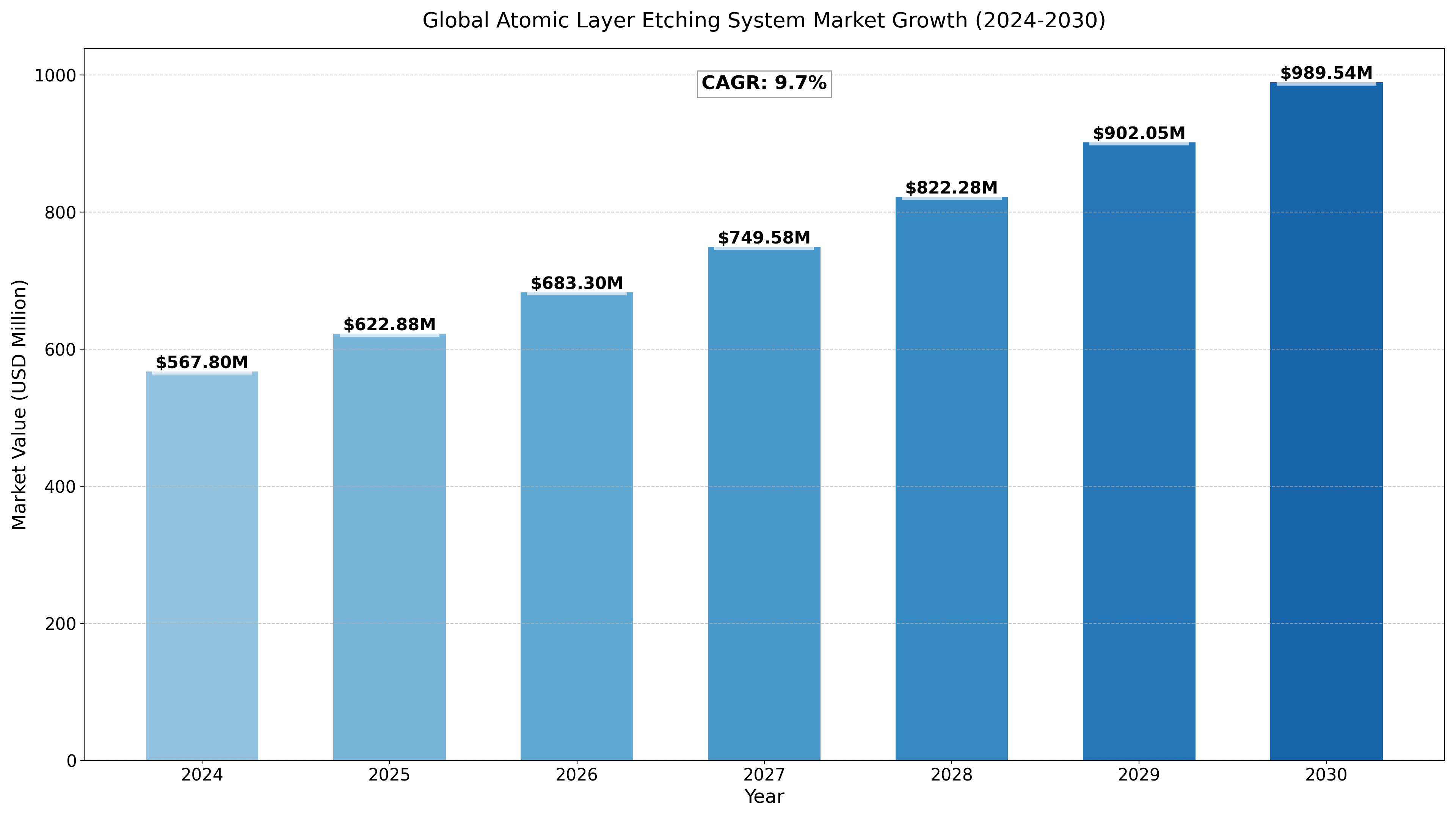
The Global Atomic Layer Etching System Market size was valued at US$ 567.8 million in 2024 and is projected to reach US$ 989.54 million by 2030, at a CAGR of 9.7% during the forecast period 2024-2030.
The United States Atomic Layer Etching System market size was valued at US$ 148.9 million in 2024 and is projected to reach US$ 252.3 million by 2030, at a CAGR of 9.2% during the forecast period 2024-2030.
Advanced semiconductor processing equipment for precise atomic-level material removal, featuring controlled etching capabilities for nanoscale device fabrication.
Report Overview
Atomic layer etch, sometimes known as ALE, is a next-generation plasma etch technology that enables layer-by-layer, or atom-by-atom, etching for IC designs.
This report provides a deep insight into the global Atomic Layer Etching System market covering all its essential aspects. This ranges from a macro overview of the market to micro details of the market size, competitive landscape, development trend, niche market, key market drivers and challenges, SWOT analysis, value chain analysis, etc.
The analysis helps the reader to shape the competition within the industries and strategies for the competitive environment to enhance the potential profit. Furthermore, it provides a simple framework for evaluating and accessing the position of the business organization. The report structure also focuses on the competitive landscape of the Global Atomic Layer Etching System Market, this report introduces in detail the market share, market performance, product situation, operation situation, etc. of the main players, which helps the readers in the industry to identify the main competitors and deeply understand the competition pattern of the market.
In a word, this report is a must-read for industry players, investors, researchers, consultants, business strategists, and all those who have any kind of stake or are planning to foray into the Atomic Layer Etching System market in any manner.
Global Atomic Layer Etching System Market: Market Segmentation Analysis
The research report includes specific segments by region (country), manufacturers, Type, and Application. Market segmentation creates subsets of a market based on product type, end-user or application, Geographic, and other factors. By understanding the market segments, the decision-maker can leverage this targeting in the product, sales, and marketing strategies. Market segments can power your product development cycles by informing how you create product offerings for different segments.
Key Company
- Lam Research
- Applied Materials
- TEL
- Hitachi High-Tech
- Oxford Instruments
- Corial
- NAURA Technology
- Market Segmentation (by Type)
- Plasma Type
- High Temperature Type
- Market Segmentation (by Application)
- Transistor
- Extreme Ultraviolet Lithography
- Other
- North America (USA, Canada, Mexico)
- Europe (Germany, UK, France, Russia, Italy, Rest of Europe)
- Asia-Pacific (China, Japan, South Korea, India, Southeast Asia, Rest of Asia-Pacific)
- South America (Brazil, Argentina, Columbia, Rest of South America)
- The Middle East and Africa (Saudi Arabia, UAE, Egypt, Nigeria, South Africa, Rest of MEA)
- Industry drivers, restraints, and opportunities covered in the study
- Neutral perspective on the market performance
- Recent industry trends and developments
- Competitive landscape & strategies of key players
- Potential & niche segments and regions exhibiting promising growth covered
- Historical, current, and projected market size, in terms of value
- In-depth analysis of the Atomic Layer Etching System Market
- Overview of the regional outlook of the Atomic Layer Etching System Market:
- Access to date statistics compiled by our researchers. These provide you with historical and forecast data, which is analyzed to tell you why your market is set to change
- This enables you to anticipate market changes to remain ahead of your competitors
- You will be able to copy data from the Excel spreadsheet straight into your marketing plans, business presentations, or other strategic documents
- The concise analysis, clear graph, and table format will enable you to pinpoint the information you require quickly
- Provision of market value (USD Billion) data for each segment and sub-segment
- Indicates the region and segment that is expected to witness the fastest growth as well as to dominate the market
- Analysis by geography highlighting the consumption of the product/service in the region as well as indicating the factors that are affecting the market within each region
- Competitive landscape which incorporates the market ranking of the major players, along with new service/product launches, partnerships, business expansions, and acquisitions in the past five years of companies profiled
- Extensive company profiles comprising of company overview, company insights, product benchmarking, and SWOT analysis for the major market players
- The current as well as the future market outlook of the industry concerning recent developments which involve growth opportunities and drivers as well as challenges and restraints of both emerging as well as developed regions
- Includes in-depth analysis of the market from various perspectives through Porters five forces analysis
- Provides insight into the market through Value Chain
- Market dynamics scenario, along with growth opportunities of the market in the years to come
- 6-month post-sales analyst support
Customization of the Report
In case of any queries or customization requirements, please connect with our sales team, who will ensure that your requirements are met.
Drivers
- Advancement in Semiconductor Fabrication: The increasing demand for smaller, faster, and more efficient semiconductor devices is a major driver for the ALE system market. As semiconductor manufacturers continue to scale down the size of transistors and integrate more components onto chips, the need for atomic-scale precision in etching processes has become essential. ALE allows for extremely precise control of material removal, enabling the production of advanced semiconductor devices like those used in 5G, AI, and quantum computing technologies.
- Miniaturization of Electronics: The trend of miniaturization across consumer electronics, particularly in smartphones, wearable devices, and IoT products, has pushed the demand for ALE systems. As components continue to shrink, conventional etching techniques cannot meet the stringent requirements of nanometer-scale precision. ALE offers a solution to this challenge, allowing for controlled etching without damaging the underlying material or surrounding structures.
- Growing Need for High-Performance Materials: ALE is crucial for fabricating advanced materials with specific properties, such as high-precision thin films, low-damage etching, and selective material removal. The market is witnessing increased demand for materials used in MEMS (Microelectromechanical Systems), photonics, and next-generation electronics, all of which benefit from ALE’s precise etching capabilities.
- Rise of 3D Integrated Circuits (3D ICs): The development of 3D ICs, which involve stacking multiple layers of semiconductor devices to enhance performance and reduce space, is another key driver for the ALE market. ALE provides the precise etching needed to fabricate these complex 3D structures, facilitating higher density, improved power efficiency, and faster processing speeds in modern electronics.
Restraints
- High Capital Costs: The initial cost of purchasing and installing ALE systems is relatively high compared to traditional etching techniques. For smaller players in the semiconductor industry or companies in developing markets, this high upfront investment may limit their ability to adopt ALE technology. The cost of maintaining these systems, which often requires highly specialized expertise, can also be a financial burden.
- Complexity of Operation and Maintenance: ALE systems are highly specialized and require skilled operators who are trained in atomic layer deposition and etching processes. The complexity of the technology means that the workforce needs to be trained to handle these systems effectively. Additionally, routine maintenance and troubleshooting of ALE systems are more demanding than traditional etching equipment, which can deter adoption.
- Limited Market Penetration in Certain Sectors: Despite its benefits in advanced semiconductor applications, ALE technology is not yet widely adopted in all industries. Certain segments of the manufacturing industry, such as mass production of simple semiconductor devices, may not require the high precision that ALE provides, limiting the growth of the market in these areas.
Opportunities
- Emerging Applications in Quantum Computing: Quantum computing is a rapidly emerging field, and ALE systems offer a critical advantage in fabricating quantum devices, where extremely precise etching and thin-film processing are required. As the market for quantum computing grows, there is a significant opportunity for ALE systems to become an essential technology in this domain.
- Development of New Materials for Advanced Technologies: ALE enables the precise etching of new materials like high-κ dielectrics, metals, and 2D materials such as graphene, which are crucial for the next generation of electronic devices. The growing focus on material innovation in semiconductors and electronics, especially in fields such as energy storage, optoelectronics, and photonic devices, presents significant growth potential for the ALE market.
- Integration with Other Nanofabrication Technologies: ALE is likely to become increasingly integrated with other advanced nanofabrication technologies such as atomic layer deposition (ALD) and molecular beam epitaxy (MBE). This integration will create hybrid systems capable of producing highly complex structures with unparalleled precision, opening up new possibilities for device design and miniaturization.
- Growing Investment in Semiconductor R&D: Increased investment in semiconductor research and development, particularly in regions like Asia-Pacific, North America, and Europe, is creating growth opportunities for the ALE system market. As manufacturers focus on developing next-generation chips, devices, and packaging technologies, ALE systems will become essential for producing the fine features required in cutting-edge semiconductors.
Challenges
- Competition from Traditional Etching Techniques: Despite its advantages, ALE faces competition from traditional etching technologies like reactive ion etching (RIE) and deep ultraviolet (DUV) lithography. These methods are more established, cost-effective, and have shorter processing times, making them attractive to companies that may not require the ultra-precision of ALE systems. Overcoming this challenge will require demonstrating the superior performance and long-term cost benefits of ALE in high-precision applications.
- Technical Limitations in Throughput: One of the primary challenges for ALE systems is their relatively low throughput compared to traditional etching methods. Since ALE operates on the atomic scale and involves sequential processes, it tends to be slower. This can be a limitation in high-volume manufacturing environments, where high production rates are essential. Overcoming this challenge and improving the scalability of ALE systems is critical for broader market adoption.
- Supply Chain and Material Constraints: The production of ALE systems depends on a specialized supply chain for high-quality materials, such as advanced etching gases and precision components. Any disruption in this supply chain, whether due to geopolitical factors or material shortages, can impact the growth and performance of the ALE system market. Manufacturers will need to ensure a robust and reliable supply chain to avoid disruptions.
- Regulatory and Environmental Concerns: As with any advanced manufacturing technology, the environmental impact of ALE systems—such as the use of etching chemicals and energy consumption—must be considered. Stricter environmental regulations and the increasing focus on sustainability may pose challenges for companies looking to implement ALE systems, especially if they require costly waste disposal and filtration technologies.

Get Sample Report PDF for Exclusive Insights
Report Sample Includes
- Table of Contents
- List of Tables & Figures
- Charts, Research Methodology, and more...