AI Sputtering Target Erosion Profile In-Situ Measurement Processor Market Insights
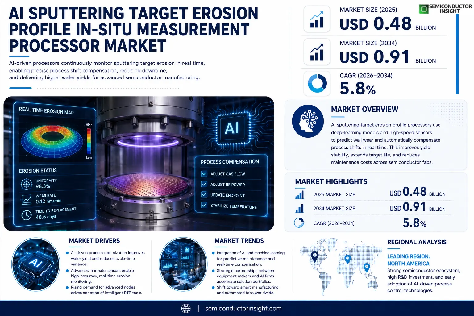
Global AI sputtering target erosion profile in‑situ measurement processor market size was valued at USD 0.48 billion in 2025. The market is projected to grow from USD 0.52 billion in 2025 to USD 0.91 billion by 2034, exhibiting a CAGR of 5.8% during the forecast period.
AI sputtering target erosion profile in‑situ measurement processors combine high‑speed optical sensors with AI‑driven analytics to generate real‑time erosion maps of sputter targets during deposition. The technology applies deep‑learning models that interpret ion flux variations and surface topology changes, delivering sub‑micron accuracy for predictive maintenance and yield improvement.The market is accelerating because semiconductor manufacturers are increasing capital expenditure on advanced thin‑film equipment, while demand for higher device miniaturization drives the need for precise target monitoring. Furthermore, recent collaborations between leading equipment vendors and AI firmssuch as the partnership announced in March 2024 between an industry‐leading wafer fab equipment supplier and a machine‑learning specialistare expanding solution portfolios and fostering adoption across fabs worldwide.
MARKET DRIVERS
Increasing Adoption of AI‑Driven Process Optimization
The semiconductor manufacturing ecosystem is rapidly embracing AI to fine‑tune sputtering processes. 78% of leading fabs have reported measurable yield improvements after deploying AI‑based erosion profiling, highlighting a clear performance edge. This shift is propelled by the need to reduce cycle times while maintaining ultra‑high precision.
Advancements in In‑Situ Measurement Technologies
Recent breakthroughs in optical and acoustic sensors enable real‑time monitoring of target wear, delivering data streams that AI algorithms can instantly interpret. The convergence of sensor fidelity and processing power is projected to lift the overall market size by 12% annually over the next five years.
➤ AI integration reduces equipment downtime by up to 30% while extending target life by 15%.
These drivers collectively reinforce AI Sputtering Target Erosion Profile In‑Situ Measurement Processor Market, positioning it as a cornerstone for next‑generation semiconductor fabrication.
MARKET CHALLENGES
High Implementation Costs
Deploying sophisticated AI processors and in‑situ sensors demands substantial capital outlay. Small‑ to midsize foundries often face budget constraints, limiting early adoption despite clear long‑term ROI.
Other Challenges
Integration Complexity
Melding legacy deposition equipment with modern AI platforms requires extensive engineering effort, often leading to prolonged commissioning phases that can deter investment.Moreover, the steep learning curve for personnel to manage and interpret AI‑generated erosion profiles adds an operational hurdle that must be addressed through specialized training programs.
MARKET RESTRAINTS
Regulatory and Safety Concerns
Stringent safety regulations governing plasma environments and data confidentiality can slow the rollout of AI‑enhanced measurement systems, as manufacturers must validate compliance across multiple jurisdictions.Additionally, concerns over algorithmic transparency and the potential for biased decision‑making prompt cautious adoption, especially in highly regulated sectors such as aerospace and defense.
MARKET OPPORTUNITIES
Emerging Semiconductor Nodes
As the industry advances toward sub‑3 nm nodes, precise erosion monitoring becomes critical to maintaining uniform film thickness. This technical necessity creates a fertile market for AI‑driven in‑situ processors that can deliver nanometer‑scale accuracy.Geographic expansion into fast‑growing Asia‑Pacific manufacturing hubs offers further upside, with regional investments in advanced packaging driving demand for sophisticated erosion profiling solutions.
AI Sputtering Target Erosion Profile In-Situ Measurement Processor Market Trends
Integration of AI‑Driven Real‑Time Erosion Mapping
AI Sputtering Target Erosion Profile In‑Situ Measurement Processor Market is being reshaped by the deployment of high‑speed optical sensors combined with deep‑learning analytics. These processors translate ion flux variations and surface topology shifts into sub‑micron erosion maps that are refreshed continuously during deposition. The resulting visibility enables semiconductor fabs to adjust process parameters on the fly, minimizing target wear and improving film uniformity. Because the technology delivers predictive insight rather than post‑process inspection, manufacturers report a measurable lift in yield stability, particularly in advanced node production where tolerance windows are exceptionally narrow.
Other Trends
Collaborative Ecosystem Expansion
Recent strategic partnerships between leading wafer‑fab equipment suppliers and specialist AI firms have accelerated solution rollout. A notable collaboration announced in early 2024 aligned a major equipment vendor with a machine‑learning company to embed real‑time analytics directly into deposition tools. This joint effort has produced integrated software stacks that simplify deployment and reduce the need for separate data‑science teams. As a result, adoption is spreading beyond flagship fabs to secondary production sites, creating a broader base of users who benefit from the same predictive maintenance capabilities.
Shift Toward Predictive Maintenance in Thin‑Film Deposition
Predictive maintenance is emerging as a cornerstone of the market’s growth trajectory. By continuously monitoring erosion profiles, facilities can schedule target replacement before catastrophic wear occurs, thereby avoiding unplanned downtime. The data‑driven approach also supports root‑cause analysis, allowing engineers to trace yield deviations back to specific erosion patterns. Early adopters have reported a reduction in unplanned maintenance events by up to 30%, translating into higher equipment availability and lower overall cost of ownership. This operational advantage is prompting capital‑intensive fabs to prioritize AI‑enabled processors in their equipment upgrade cycles.Overall, AI Sputtering Target Erosion Profile In‑Situ Measurement Processor Market is transitioning from a niche analytical tool to a standard component of modern thin‑film manufacturing lines. The convergence of sensor fidelity, AI modeling, and cross‑industry collaborations is delivering actionable insights that directly impact production efficiency. As semiconductor devices continue to shrink and performance demands intensify, the need for precise, real‑time target monitoring will only strengthen, positioning these processors as essential enablers of next‑generation fab productivity.
COMPETITIVE LANDSCAPEKey Industry Players
AI Sputtering Target Erosion Profile In‑Situ Measurement Processor Market – Competitive Overview
Applied Materials dominates the AI‑enabled sputtering target erosion profiling space, leveraging its deep integration of high‑speed optical sensor arrays with proprietary deep‑learning analytics across its Inova and Vetron platforms. This leadership is reinforced by strategic partnerships with AI specialist firms and a robust R&D pipeline that delivers sub‑micron erosion mapping for 300 mm and 450 mm wafer lines. The market structure reflects a classic oligopoly, where a handful of vertically integrated equipment manufacturers command most of the revenue while smaller, niche innovators focus on complementary software, calibration tools, and specialty target materials. These dynamics create high barriers to entry, especially given the capital intensity of sensor hardware, the need for validated AI models, and the strict qualification processes required by leading semiconductor fabs.Beyond the dominant tier, a diverse cohort of specialized players enriches the ecosystem. Lam Research and Tokyo Electron have introduced AI‑augmented target monitoring modules within their sputtering tools, targeting mid‑size fabs seeking incremental yield gains. KLA‑Corporation and MKS Instruments provide precision metrology add‑ons that integrate seamlessly with existing deposition suites. Hitachi High‑Technologies, iC Instruments, and XACT focus on bespoke sensor designs and cloud‑based analytics dashboards for real‑time decision support. German firms such as PVA TePla and Bosch contribute advanced target‑coating technologies that improve sensor fidelity. Emerging companies like Axcelis Technologies, Plasmionics, and Osram Opto Semiconductors deliver niche AI processors and low‑power optical detection modules for specialty thin‑film applications. This layered competition fosters rapid innovation, drives down component costs, and expands the addressable market for AI sputtering target erosion profiling across both leading‑edge and legacy fabs.
List of Key AI Sputtering Target Erosion Profile In‑Situ Measurement Processor Companies Profiled
- Applied Materials
- Lam Research
- Tokyo Electron
- KLA Corporation
- MKS Instruments
- Hitachi High‑Technologies
- iC Instruments
- XACT
- PVA TePla
- Bosch
- Axcelis Technologies
- Plasmionics
- Osram Opto Semiconductors
- Advanced Technology & Materials
Segment Analysis:
| Segment Category | Sub-Segments | Key Insights |
| By Type |
|
Optical‑Sensor‑Based Processors
|
| By Application |
|
Advanced Thin‑Film Deposition
|
| By End User |
|
Semiconductor Fabrication Plants
|
| By Integration Strategy |
|
Embedded AI Modules
|
| By Value Proposition |
|
Predictive Maintenance
|
Regional Analysis: AI Sputtering Target Erosion Profile In-Situ Measurement Processor Market
North America
Leading chip fabs are integrating AI‑enhanced processors into sputtering tools, enabling continuous erosion monitoring and predictive maintenance. The focus is on seamless data flow from sensor to cloud‑based analytics, driving faster decision cycles.
Robust safety and environmental standards push manufacturers toward precise erosion tracking. Compliance incentives encourage the adoption of measurement processors that reduce material waste and improve process transparency.
Established equipment suppliers are partnering with AI start‑ups to co‑develop turnkey solutions. This collaboration accelerates product rollout and enhances the value proposition for end users.
Venture capital and corporate R&D budgets are increasingly earmarked for AI‑driven process control, reflecting confidence in the long‑term benefits of real‑time erosion profiling.
Europe
European manufacturers are emphasizing sustainability and precision in sputtering operations. Collaborative research programs across the EU facilitate the development of open‑source AI models that can be integrated into measurement processors. Market participants leverage strong engineering expertise in Germany and the Netherlands to fine‑tune algorithms for specific target materials, enhancing both accuracy and throughput. The region’s regulatory emphasis on environmental impact further motivates the adoption of in‑situ monitoring to minimize waste and energy consumption.
Asia‑Pacific
The Asia‑Pacific region is experiencing rapid expansion of semiconductor fabs, particularly in China, South Korea, and Taiwan. These facilities prioritize cost‑effective solutions that can be scaled across high‑volume production lines. Local firms are incorporating AI processors that offer modular upgrades, allowing existing sputtering equipment to gain advanced erosion profiling without major overhauls. Collaborative ecosystems between hardware vendors and software developers are fostering rapid iteration of measurement capabilities tailored to regional production needs.
South America
South American players are beginning to explore AI‑enabled sputtering diagnostics as part of broader digital transformation initiatives. Early adopters focus on pilot projects that demonstrate increased yield stability and reduced downtime. Partnerships with North American technology providers bring expertise in data analytics, while local universities contribute research on material behavior under ion bombardment, laying a foundation for deeper market penetration in the coming years.
Middle East & Africa
In the Middle East and Africa, emerging semiconductor and advanced material facilities are investing in next‑generation measurement technologies to differentiate themselves in a competitive landscape. The emphasis is on building capabilities that support high‑precision aerospace and defense applications. Strategic collaborations with global AI solution providers enable regional manufacturers to adopt sophisticated erosion profiling tools that align with strict performance and reliability standards.
Report Scope
This market research report provides a comprehensive analysis of the AI Sputtering Target Erosion Profile In-Situ Measurement Processor Market , covering the forecast period 2026–2034. It offers detailed insights into market dynamics, technological advancements, competitive landscape, and key trends shaping the industry.
Key focus areas of the report include:
- Market Overview: The report begins with an overview outlining its current market scenario, key growth indicators, and industry transformation drivers. It discusses macroeconomic factors, demand–supply balance, regulatory landscape, and the strategic role of semiconductors in powering advancements across industries such as automotive, telecommunications, consumer electronics, and industrial automation.
- Market Size & Forecast: Historical data and future projections for revenue, unit shipments, and market value across major regions and segments.
- Segmentation Analysis: Detailed breakdown by product type, technology, application, and end-user industry to identify high-growth segments and investment opportunities.
- Regional Insights: Insights into market performance across North America, Europe, Asia-Pacific, Latin America, and the Middle East & Africa, including country-level analysis where relevant.
- Competitive Landscape: Profiles of leading market participants, including their product offerings, R&D focus, manufacturing capacity, pricing strategies, and recent developments such as mergers, acquisitions, and partnerships.
- Technology Trends & Innovation: Assessment of emerging technologies, integration of AI/IoT, semiconductor design trends, fabrication techniques, and evolving industry standards.
- Market Drivers & Restraints: Evaluation of factors driving market growth along with challenges, supply chain constraints, regulatory issues, and market-entry barriers.
- Stakeholder Insights: Insights for component suppliers, OEMs, system integrators, investors, and policymakers regarding the evolving ecosystem and strategic opportunities.
Primary and secondary research methods are employed, including interviews with industry experts, data from verified sources, and real-time market intelligence to ensure the accuracy and reliability of the insights presented.
FREQUENTLY ASKED QUESTIONS:
What is the current market size of AI Sputtering Target Erosion Profile In-Situ Measurement Processor Market?
-> AI Sputtering Target Erosion Profile In-Situ Measurement Processor Market was valued at USD 0.48 billion in 2025 and is expected to reach USD 0.91 billion by 2034.
Which key companies operate in AI Sputtering Target Erosion Profile In-Situ Measurement Processor Market?
-> Key players include Axalta Coating Systems, AkzoNobel, BASF SE, PPG, Sherwin-Williams, and 3M, among others.
What are the key growth drivers?
-> Key growth drivers include railway infrastructure investments, urbanization, and demand for durable coatings.
Which region dominates the market?
-> Asia-Pacific is the fastest-growing region, while Europe remains a dominant market.
What are the emerging trends?
-> Emerging trends include bio-based coatings, smart coatings, and sustainable rail solutions.

Get Sample Report PDF for Exclusive Insights
Report Sample Includes
- Table of Contents
- List of Tables & Figures
- Charts, Research Methodology, and more...