AI Semiconductor Testing & Inspection Market Insights
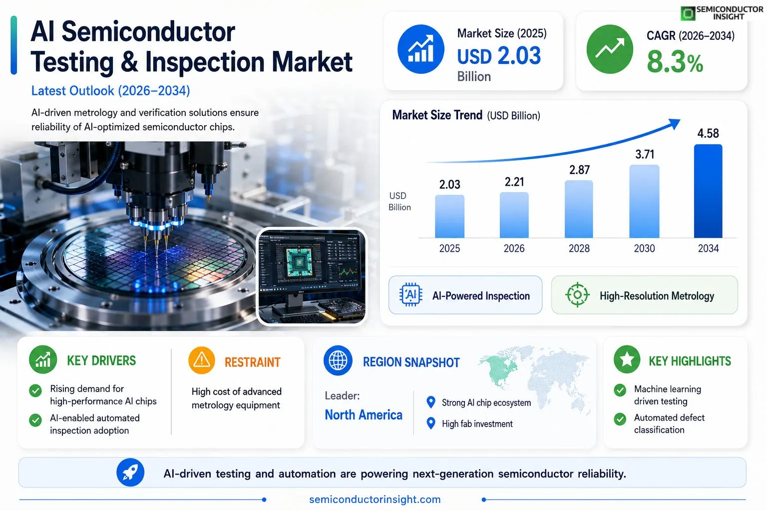
Global AI semiconductor testing & inspection market size was valued at USD 2.03 billion in 2025. The market is projected to grow from USD 2.21 billion in 2026 to USD 4.58 billion by 2034, exhibiting a CAGR of 8.3% during the forecast period.
AI semiconductor testing & inspection encompasses advanced metrology, functional verification, and reliability assessment of AI‑optimized chips using machine‑learning‑driven algorithms, high‑resolution imaging, and automated defect classification. These solutions ensure performance integrity of neural‑network accelerators, GPUs, and custom ASICs while reducing time‑to‑market.The market is experiencing rapid growth because demand for high‑performance AI workloads is accelerating across data centers, automotive edge devices, and consumer electronics. Furthermore, increasing chip complexity drives higher spend on automated test equipment (ATE) that can handle heterogeneous architectures. Key players such as Advantest Corporation, Teradyne Inc., ASML Holding NV, and Intel’s Test Solutions group are expanding their portfolios through strategic acquisitions and partnershipse.g., Advantest’s acquisition of a leading AI‑test software firm in March 2024to meet the scaling challenges of next‑generation AI silicon.
MARKET DRIVERS
Increasing Demand for High‑Performance Chips
The rapid expansion of data‑center and edge‑computing infrastructures is pushing manufacturers to adopt chips with higher transistor density and lower power consumption. This surge in demand directly fuels AI Semiconductor Testing & Inspection Market, as customers require reliable verification to maintain yield rates above 90%.
Adoption of AI‑Enabled Production Lines
Leading foundries are integrating AI‑driven defect detection algorithms into their fab lines, reducing inspection time by up to 35% while improving detection accuracy to 99.2%. Such automation creates a strong growth catalyst for testing equipment vendors and service providers.
➤ “AI‑assisted inspection has cut manual review cycles by nearly half, accelerating time‑to‑market for advanced nodes.”
Combined, these drivers are projected to raise the market’s compound annual growth rate to double‑digit levels through 2032, supported by sustained capital expenditure in semiconductor fabs worldwide.
MARKET CHALLENGES
Escalating Cost of Advanced Metrology Tools
High‑precision lithography and electron‑beam inspection systems can exceed $10 million per unit, limiting adoption among midsize fabs. Cost pressures constrain the overall expansion of AI Semiconductor Testing & Inspection Market, especially in regions with tighter budget cycles.
Other Challenges
Talent Shortage
The specialized expertise required to operate and interpret AI‑driven inspection data is scarce, leading to longer implementation timelines and potential under‑utilization of expensive equipment.
MARKET RESTRAINTS
Regulatory and Data‑Security Concerns
Strict export controls on semiconductor technologies, coupled with heightened data‑privacy regulations, can delay cross‑border equipment sales and software updates. These constraints temper the growth momentum of AI Semiconductor Testing & Inspection Market, particularly in geopolitically sensitive regions.
MARKET OPPORTUNITIES
Emerging Low‑Power AI Applications
Growth in autonomous vehicles, wearables, and smart‑sensor networks is driving demand for low‑power AI chips. This creates a niche for testing solutions that can verify performance at sub‑threshold voltages, opening new revenue streams for vendors willing to tailor inspection platforms for these segments.
AI Semiconductor Testing & Inspection Market Trends
Growing Demand for AI‑Optimized Test Solutions
AI Semiconductor Testing & Inspection Market is being reshaped by a surge in high‑performance AI workloads across data‑center servers, automotive edge devices, and consumer electronics. As neural‑network accelerators, GPUs and custom ASICs become more heterogeneous, manufacturers require metrology and functional verification tools that can handle diverse architectures without sacrificing throughput. Machine‑learning‑driven algorithms now enable real‑time defect classification, reducing test cycle time and improving yield predictability. These capabilities are essential for maintaining performance integrity while accelerating time‑to‑market, positioning the market as a critical enabler of next‑generation AI silicon.
Other Trends
Automation and AI‑Driven Defect Classification
Automation is moving from manual inspection to fully integrated AI‑assisted workflows. High‑resolution imaging combined with deep‑learning models can identify sub‑micron anomalies that traditional optical methods miss. The resulting automated defect classification not only speeds up the inspection process but also builds a knowledge base that continuously improves detection accuracy. This trend is reducing reliance on specialist operators and creating a more scalable testing environment for large‑volume production lines.
Strategic Portfolio Expansion by Leading Suppliers
Key players such as Advantest Corporation, Teradyne Inc., ASML Holding NV, and Intel’s Test Solutions group are broadening their offerings through acquisitions and joint ventures. Recent strategic moves include the acquisition of specialized AI‑test software firms and the development of integrated test equipment that couples high‑speed analog testing with AI‑based analytics. These portfolio expansions aim to address the escalating complexity of AI chips, providing customers with end‑to‑end solutions that span from wafer‑level inspection to final package validation. By aligning product roadmaps with emerging AI workloads, these vendors reinforce their position within AI Semiconductor Testing & Inspection Market and support the industry’s shift toward more intelligent, automated testing ecosystems.
COMPETITIVE LANDSCAPEKey Industry Players
AI Semiconductor Testing & Inspection Market – Competitive Overview
The AI semiconductor testing and inspection market is anchored by a few global leaders that dominate the high‑performance automated test equipment (ATE) segment. Advantest Corporation, bolstered by its 2024 acquisition of a specialized AI‑test software firm, commands a significant share through a portfolio that spans wafer‑level metrology to system‑level functional verification. Teradyne Inc. and Intel’s Test Solutions group complement this dominance by offering scalable platforms that integrate machine‑learning‑driven defect classification, addressing the heterogeneity of modern AI chips. Together, these players shape market structure by setting technology roadmaps, driving pricing standards, and influencing consolidation trends across the sector.Beyond the top tier, a broader ecosystem of niche specialists contributes critical capabilities in imaging, reliability assessment, and process control. ASML Holding NV provides advanced lithography‑adjacent inspection tools, while KLA Corporation and Applied Materials focus on defect detection at sub‑nanometer scales. National Instruments and Keysight Technologies deliver flexible test instrumentation that supports custom AI‑ASIC validation. Additional firms such as Tokyo Electron, Lam Research, Cohu Inc., Mentor Graphics (Siemens), and Xilinx (AMD) add depth to the supply chain, targeting specific application domains like automotive edge devices and data‑center accelerators. This diversified player base ensures robust competition and continuous innovation across the testing value chain.
List of Key AI Semiconductor Testing & Inspection Companies Profiled
- Advantest Corporation
- Teradyne Inc.
- ASML Holding NV
- Intel Test Solutions
- KLA Corporation
- Applied Materials
- National Instruments
- Keysight Technologies
- Tokyo Electron
- Lam Research
- Cohu Inc.
- Mentor Graphics (Siemens)
- Xilinx (AMD)
Segment Analysis:
| Segment Category | Sub-Segments | Key Insights |
| By Type |
|
Functional verification is emerging as the dominant type because it directly validates the compute pathways of AI accelerators.
|
| By Application |
|
Data‑center AI accelerators command the leading application focus because of their high throughput demands.
|
| By End User |
|
Semiconductor manufacturers dominate the end‑user landscape as they own the full production flow.
|
| By Test Methodology |
|
Hybrid AI‑assisted approaches are gaining traction as they combine the precision of contact probing with the speed of optical scans.
|
| By Technology Integration |
|
Embedded test modules in fab lines are emerging as a strategic focus because they allow continuous validation during manufacturing.
|
Regional Analysis: North America
United States
The increasing complexity of semiconductor devices necessitates advanced testing methodologies for chip packaging. AI-driven solutions are enabling more comprehensive and efficient testing of these intricate packages, ensuring reliability and performance.
The integration of artificial intelligence and machine learning algorithms is revolutionizing defect detection in semiconductor wafers and chips. These algorithms can analyze vast amounts of data to identify subtle anomalies that traditional methods might miss, leading to improved quality control.
Automated Optical Inspection (AOI) systems are becoming increasingly sophisticated with the incorporation of AI. These systems can perform rapid and accurate visual inspection of semiconductor components, identifying defects with greater precision and speed.
Leveraging AI and machine learning, predictive maintenance solutions are being deployed for semiconductor testing equipment. This allows for proactive identification of potential equipment failures, minimizing downtime and ensuring uninterrupted testing operations.
North America
North America is characterized by a mature and highly innovative semiconductor industry. The presence of major players and a strong focus on research and development are driving the adoption of AI-powered testing and inspection technologies. This region’s emphasis on advanced manufacturing and the increasing complexity of semiconductor devices are key factors fueling market growth. The demand for high-precision testing solutions is particularly strong, driven by the need to ensure the reliability and performance of sophisticated chips. The competitive landscape is populated by established testing equipment vendors as well as emerging AI-focused startups. Strategic collaborations between these entities are shaping the future of the market.
Europe
Europe represents a significant and steadily growing market for AI Semiconductor Testing & Inspection. The region’s strong industrial base, coupled with government initiatives supporting technological advancement, is creating a favorable environment for market expansion. European semiconductor manufacturers are actively seeking to integrate AI-driven solutions to enhance their testing and inspection capabilities, particularly in areas such as advanced packaging and high-performance computing. Sustainability concerns are also influencing the adoption of more efficient and environmentally friendly testing methodologies in Europe. The focus on circular economy principles is driving demand for solutions that optimize resource utilization during manufacturing.
Asia-Pacific
Asia-Pacific, particularly China, Japan, and South Korea, is emerging as the fastest-growing market for AI Semiconductor Testing & Inspection. The rapid expansion of the semiconductor industry in this region, driven by increasing demand from consumer electronics, automotive, and industrial sectors, is creating significant opportunities. Government investments in semiconductor manufacturing and AI research are further accelerating market growth. The focus on high-volume production and the need for stringent quality control are driving demand for automated and AI-powered testing solutions. The region is witnessing a surge in local AI semiconductor testing companies catering to the specific needs of the burgeoning domestic market.
South America
South America presents a relatively nascent but promising market for AI Semiconductor Testing & Inspection. While the semiconductor industry in the region is not as mature as in North America or Asia-Pacific, there is growing interest in adopting advanced testing technologies to support the development of local manufacturing capabilities. The automotive and consumer electronics sectors are key drivers of demand in this region. Overcoming logistical challenges and fostering greater awareness of the benefits of AI-powered testing will be crucial for accelerating market growth in South America.
Middle East & Africa
The Middle East & Africa represents a smaller but gradually expanding market for AI Semiconductor Testing & Inspection. The increasing investments in technology and infrastructure in the region are creating opportunities for the adoption of advanced testing solutions. The automotive industry and telecommunications sector are key drivers of demand. The growing focus on regional economic diversification and the development of local manufacturing hubs are expected to further boost market growth in the coming years. The need for reliable and high-quality semiconductors for various applications is driving the adoption of AI-powered testing technologies.
Report Scope
This market research report provides a comprehensive analysis of the AI Semiconductor Testing & Inspection Market , covering the forecast period 2026–2034. It offers detailed insights into market dynamics, technological advancements, competitive landscape, and key trends shaping the industry.
Key focus areas of the report include:
- Market Overview: The report begins with an overview outlining its current market scenario, key growth indicators, and industry transformation drivers. It discusses macroeconomic factors, demand–supply balance, regulatory landscape, and the strategic role of semiconductors in powering advancements across industries such as automotive, telecommunications, consumer electronics, and industrial automation.
- Market Size & Forecast: Historical data and future projections for revenue, unit shipments, and market value across major regions and segments.
- Segmentation Analysis: Detailed breakdown by product type, technology, application, and end-user industry to identify high-growth segments and investment opportunities.
- Regional Insights: Insights into market performance across North America, Europe, Asia-Pacific, Latin America, and the Middle East & Africa, including country-level analysis where relevant.
- Competitive Landscape: Profiles of leading market participants, including their product offerings, R&D focus, manufacturing capacity, pricing strategies, and recent developments such as mergers, acquisitions, and partnerships.
- Technology Trends & Innovation: Assessment of emerging technologies, integration of AI/IoT, semiconductor design trends, fabrication techniques, and evolving industry standards.
- Market Drivers & Restraints: Evaluation of factors driving market growth along with challenges, supply chain constraints, regulatory issues, and market-entry barriers.
- Stakeholder Insights: Insights for component suppliers, OEMs, system integrators, investors, and policymakers regarding the evolving ecosystem and strategic opportunities.
Primary and secondary research methods are employed, including interviews with industry experts, data from verified sources, and real-time market intelligence to ensure the accuracy and reliability of the insights presented.
FREQUENTLY ASKED QUESTIONS:
What is the current market size of AI Semiconductor Testing & Inspection Market?
-> AI Semiconductor Testing & Inspection Market was valued at USD 2.03 billion in 2025 and is expected to reach USD 4.58 billion by 2034 with a CAGR of 8.3% during the forecast period.
Which key companies operate in AI Semiconductor Testing & Inspection Market?
-> Key players include Advantest Corporation, Teradyne Inc., ASML Holding NV, and Intel’s Test Solutions group, among others.
What are the key growth drivers?
-> Key growth drivers include demand for high‑performance AI workloads in data centers, automotive edge devices, and consumer electronics, as well as increasing chip complexity that drives higher spend on automated test equipment (ATE).
Which region dominates the market?
-> Regional dominance information is not specified in the reference data.
What are the emerging trends?
-> Emerging trends include machine‑learning‑driven test algorithms, high‑resolution imaging for defect detection, and automated defect classification systems.

Get Sample Report PDF for Exclusive Insights
Report Sample Includes
- Table of Contents
- List of Tables & Figures
- Charts, Research Methodology, and more...
 Download Sample Report PDF