
AI-Driven Plasma Etch Endpoint Detection Market Insights
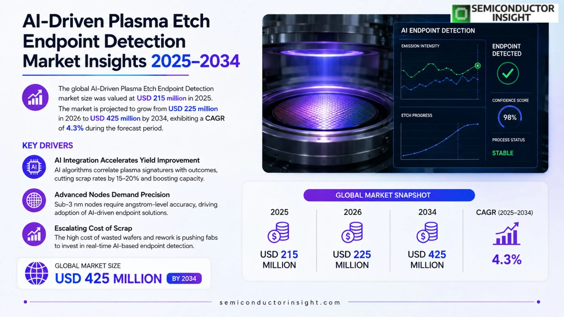
Global AI-Driven Plasma Etch Endpoint Detection market size was valued at USD 215 million in 2025. The market is projected to grow from USD 225 million in 2026 to USD 425 million by 2034, exhibiting a CAGR of 4.3% during the forecast period.
AI‑driven plasma etch endpoint detection describes systems that apply machine‑learning models to real‑time optical emission or mass‑spectrometry signals, identifying the exact point at which an etching cycle reaches its target depth or profile. By autonomously terminating or adjusting the plasma based on predictive analytics, these solutions improve wafer yield, curtail over‑etch defects, and reduce consumable costs.
The sector is accelerating because semiconductor fabs are transitioning to sub‑3 nm technologies where process margins are extremely tight and conventional manual monitoring cannot keep pace. In addition, the integration of AI into fab automation,highlighted by Applied Materials’ collaboration with IBM announced in March 2024,has spurred capital spending on intelligent endpoint tools. Established players such as Lam Research, Tokyo Electron Limited and KLA Corporation are broadening their offerings with AI‑enhanced modules, further propelling adoption.
MARKET DRIVERS
AI Integration Accelerates Yield Improvement
Semiconductor fabs are increasingly turning to AI algorithms to interpret plasma etch signatures. By correlating optical emission data with historical run‑to‑run outcomes, manufacturers can pinpoint the exact moment when a feature reaches its target dimensions. This precision cuts scrap rates by 15‑20%, allowing line managers to meet aggressive capacity targets without expanding clean‑room footprints.
Cost Pressures Favor Automated Endpoint Detection
Rising equipment depreciation and labor shortages compel fabs to replace manual monitoring with AI‑driven solutions. Automated systems reduce the need for specialist technologists on the floor, trimming operational expenses by an estimated 12% per wafer lot. The savings translate into tighter product pricing windows, especially for high‑mix, low‑volume applications.
➤ “Deploying machine‑learning models for endpoint detection has shaved 30 seconds off cycle time on a typical 200 mm tool, directly boosting throughput.”
These efficiencies are reshaping capital allocation strategies. Investors now view the AI-Driven Plasma Etch Endpoint Detection Market as a lever for margin expansion rather than a peripheral add‑on, prompting a surge in vendor R&D budgets aimed at real‑time analytics.
MARKET CHALLENGES
Data Quality and Model Generalization
High‑volume etch processes generate terabytes of sensor data, yet inconsistencies across toolsets create noisy inputs for AI models. When a model trained on one equipment family is applied to another, prediction accuracy can dip below 70%, forcing firms to invest in extensive retraining cycles.
Other Challenges
Integration with Legacy MES
Legacy Manufacturing Execution Systems (MES) often lack open APIs, making seamless data exchange cumbersome. The resulting siloed architecture hampers real‑time decision making, slowing adoption rates among mid‑size fabs.
MARKET RESTRAINTS
Regulatory Scrutiny on AI Transparency
Regulators in major semiconductor hubs are beginning to demand explainability for AI‑based process controls. Firms must document model rationale and provide audit trails, which adds compliance overhead and can deter early‑stage adopters.
High Up‑Front Integration Costs
Embedding AI modules into existing etch lines frequently requires hardware upgrades, such as edge‑computing units and high‑speed data links. Capital outlays can reach $2‑3 million per line, a figure that constrains rollout in cost‑sensitive regions.
MARKET OPPORTUNITIES
Predictive Maintenance Coupled with Endpoint Detection
Vendors that fuse endpoint detection with predictive maintenance analytics can offer a unified dashboard that anticipates tool degradation while optimizing etch termination. This combined value proposition appeals to fabs aiming to maximize equipment uptime.
Expansion into Advanced Nodes
As process nodes shrink below 5 nm, margin for error narrows dramatically. AI‑enhanced detection becomes a prerequisite for achieving the sub‑nanometer tolerances required in 3‑D stacking and gate‑all‑around architectures, opening a rapidly growing niche for specialized providers.
Service‑Based Business Models
Shifting from perpetual licenses to subscription‑based analytics platforms lowers entry barriers for smaller fabs. Recurring revenue streams also encourage vendors to continuously refine algorithms, fostering a virtuous cycle of performance improvement.
AI-Driven Plasma Etch Endpoint Detection Market Trends
AI Integration Tightens Process Control in Sub‑3 nm Fab Operations
The semiconductor foundry environment is embracing AI‑enhanced endpoint detection as a response to the narrowing tolerances required for sub‑3 nm node production. Machine‑learning models now parse optical emission and mass‑spectrometry streams in real time, pinpointing the precise moment when etching reaches the intended depth. This capability eliminates the lag inherent in manual observation, curtails over‑etch incidents, and translates directly into higher wafer yield. The shift is not merely technological; it reshapes the cost structure of fab lines by reducing consumable waste and minimizing re‑work cycles.
Other Trends
Strategic Alliances Accelerate Tool Adoption
Partnerships such as the March 2024 collaboration between Applied Materials and IBM signal a broader industry movement toward integrated AI platforms. These alliances combine equipment expertise with advanced analytics, shortening development cycles for intelligent endpoint modules. As providers embed AI blocks into existing hardware stacks, customers can upgrade without overhauling their production footprint, making the transition financially palatable for mid‑size facilities.
Competitive Landscape Expands with AI‑Enhanced Offerings
Legacy equipment manufacturers,including Lam Research, Tokyo Electron Limited, and KLA Corporation,are augmenting their portfolios with AI‑driven detection capabilities. By retrofitting proven plasma etch tools with predictive analytics, they leverage established service networks while delivering the next generation of process assurance. The competitive thrust forces newcomers to differentiate through niche algorithms or specialized sensor configurations, fostering a diverse ecosystem of solutions that cater to varying fab philosophies.
COMPETITIVE LANDSCAPE
Key Industry Players
AI‑Driven Plasma Etch Endpoint Detection Market Competitive Overview
The market is dominated by a handful of semiconductor equipment giants that have integrated machine‑learning engines into their etch control portfolios. Lam Research, leveraging its deep etch expertise, has introduced a predictive analytics module that directly ties optical emission spectra to endpoint decisions, thereby tightening process windows for sub‑3 nm nodes. Tokyo Electron follows a similar path, embedding AI routines into its “ET” series to reduce over‑etch variance across high‑volume fabs. KLA Corporation, traditionally a metrology leader, now offers a hybrid sensor‑fusion platform that correlates mass‑spectrometry data with image‑based inspection, delivering a unified endpoint signal. Applied Materials has accelerated its AI roadmap through a strategic partnership with IBM, embedding cloud‑native models into its plasma etch suite to enable remote tuning and rapid recipe iteration. Collectively, these leaders shape a tiered ecosystem where scaling economics and software licensing dominate revenue flows, while their extensive service networks lock in long‑term customer relationships.
Beyond the tier‑one firms, a constellation of specialist and regional vendors is expanding the solution set with niche capabilities. Hitachi High‑Tech supplies high‑resolution spectrometers that feed custom neural‑net models for niche memory processes. MKS Instruments contributes precision gas‑flow sensors that improve data fidelity for AI inference. Teradyne and Advantest, though known for test equipment, are entering the domain by offering AI‑enhanced diagnostic kits that complement existing fab automation stacks. ASML’s recent foray into process‑monitoring optics, SMEE’s domestically produced plasma tools, and Nikon’s image‑analysis algorithms each add a layer of competitive pressure, especially in emerging Asian fabs where cost‑sensitive adoption is accelerating.
List of Key AI-Driven Plasma Etch Endpoint Detection Companies Profiled
- Lam Research
- Tokyo Electron Limited
- KLA Corporation
- Applied Materials
- Hitachi High‑Tech Corporation
- MKS Instruments, Inc.
- Teradyne, Inc.
- Advantest Corporation
- ASML Holding N.V.
- SMEE (Shanghai Micro Electronics Equipment Co., Ltd.)
- Nikon Corporation
- Intel Corporation
- Samsung Electronics
- GlobalFoundries
Segment Analysis:
| Segment Category | Sub-Segments | Key Insights |
| By Type |
|
Optical Emission‑Based Detection is emerging as the leading type because it integrates seamlessly with existing lithography line‑ups, provides rapid signal acquisition, and enables AI models to learn from rich spectral patterns. • Firms prioritize this type for its lower retro‑fit cost and high compatibility with current fab equipment. • The richness of real‑time emission data fuels more accurate endpoint predictions, reducing over‑etch defects. • Continuous learning loops improve process stability as device geometries shrink. |
| By Application |
|
Advanced Logic Devices dominate the application landscape as sub‑3 nm nodes demand ultra‑precise endpoint control. • AI‑driven detection allows tighter process windows, supporting the aggressive scaling roadmap. • The capability to auto‑adjust plasma parameters in‑situ aligns with the high‑volume manufacturing cadence of leading logic fabs. • Enhanced defect mitigation directly contributes to higher wafer yields, a critical factor for cost‑sensitive high‑performance chips. |
| By End User |
|
Foundries are the primary adopters because they serve multiple customers and require flexible, scalable endpoint solutions. • The modular AI architecture enables rapid deployment across heterogeneous process flows. • Predictive analytics reduce downtime and maintenance cycles, aligning with the high‑throughput demands of contract manufacturing. • Collaborative development with equipment vendors accelerates feature integration, fostering a robust ecosystem. |
| By Technology |
|
Deep Learning Models lead the technology segment because they excel at extracting intricate patterns from high‑dimensional spectral data. • Large training datasets from multiple fabs enable models to generalize across equipment variations. • Continuous retraining mechanisms keep the system aligned with evolving process recipes. • Integration with edge‑computing nodes minimizes latency, ensuring real‑time endpoint decisions. |
| By Process Stage |
|
Mid‑process Monitoring emerges as the critical stage where AI‑driven detection adds the most value. • Real‑time adjustments prevent drift, preserving the tight critical dimension budgets of sub‑nanometer layers. • The feedback loop enhances process repeatability across wafer lots. • Insightful visual dashboards empower process engineers to proactively intervene before defects manifest. |
Regional Analysis: AI-Driven Plasma Etch Endpoint Detection Market
Chipmakers are embedding neural‑network models into plasma etch controllers to recognize subtle variations in photon emission spectra. This shift reduces reliance on manual calibration, shortens cycle time, and delivers more consistent critical dimension control across high‑volume production lines.
The regional supply chain has adapted to the demand for high‑performance GPUs and ASICs that power AI inference at the edge. Partnerships with domestic silicon foundries mitigate lead‑time risks, while specialized consumables are being reformulated to support algorithm‑driven diagnostics.
Federal initiatives encouraging advanced manufacturing encourage data‑centric process monitoring. While no specific AI‑etching standards exist yet, existing semiconductor safety guidelines are being interpreted to accommodate real‑time analytics, shaping compliance strategies for equipment vendors.
Operators prioritize yield predictability and reduced downtime. The ability of AI algorithms to flag drift before it impacts product quality aligns with cost‑of‑ownership concerns, driving procurement decisions toward integrated endpoint detection platforms.
Europe
European semiconductor fabs are leveraging AI-Driven Plasma Etch Endpoint Detection Market to address stringent quality standards imposed by automotive and industrial IoT applications. Closely knit clusters in Germany and the Netherlands benefit from strong public‑private research consortia that blend AI expertise with process engineering. Companies are cautious, emphasizing validation against legacy metrology, yet the promise of lower wafer loss is prompting pilot deployments. Local policy incentives aimed at sustaining chip sovereignty further nudge manufacturers toward home‑grown AI analytics, reinforcing a gradual but steady adoption curve.
Asia‑Pacific
In the Asia‑Pacific basin, rapid expansion of wafer capacity in Taiwan, South Korea, and increasingly in China fuels interest in AI‑enabled etch monitoring. Manufacturers are dealing with intense pressure to scale while maintaining defect‑free outputs, making endpoint detection a strategic differentiator. However, divergent standards across jurisdictions and the scarcity of AI talent in some markets create implementation friction. Joint ventures between equipment giants and regional AI startups are emerging as a workaround, delivering tailored models that respect local process nuances.
South America
South American semiconductor activity remains nascent, yet niche players focusing on display driver ICs are experimenting with AI‑driven endpoint detection to improve yield on modest fab footprints. The region’s limited access to high‑end computational hardware forces reliance on cloud‑based inference, raising data‑security considerations. Partnerships with North American service providers are introducing best‑practice workflows, slowly building a foundation for broader market participation.
Middle East & Africa
The Middle East & Africa region is characterized by emerging manufacturing hubs that are positioning themselves as alternative sources for mature‑node production. Early adopters are attracted by the ability of AI‑enhanced etch monitoring to compensate for older equipment that lacks built‑in diagnostics. Government‑backed technology parks are fostering collaborations between local enterprises and global AI vendors, aiming to leapfrog traditional process control methods. While scale remains limited, the strategic focus on data‑driven reliability signals a long‑term commitment to AI-Driven Plasma Etch Endpoint Detection Market.
Report Scope
This market research report provides a comprehensive analysis of the AI-Driven Plasma Etch Endpoint Detection Market , covering the forecast period 2026–2034. It offers detailed insights into market dynamics, technological advancements, competitive landscape, and key trends shaping the industry.
Key focus areas of the report include:
- Market Overview: The report begins with an overview outlining its current market scenario, key growth indicators, and industry transformation drivers. It discusses macroeconomic factors, demand–supply balance, regulatory landscape, and the strategic role of semiconductors in powering advancements across industries such as automotive, telecommunications, consumer electronics, and industrial automation.
- Market Size & Forecast: Historical data and future projections for revenue, unit shipments, and market value across major regions and segments.
- Segmentation Analysis: Detailed breakdown by product type, technology, application, and end-user industry to identify high-growth segments and investment opportunities.
- Regional Insights: Insights into market performance across North America, Europe, Asia-Pacific, Latin America, and the Middle East & Africa, including country-level analysis where relevant.
- Competitive Landscape: Profiles of leading market participants, including their product offerings, R&D focus, manufacturing capacity, pricing strategies, and recent developments such as mergers, acquisitions, and partnerships.
- Technology Trends & Innovation: Assessment of emerging technologies, integration of AI/IoT, semiconductor design trends, fabrication techniques, and evolving industry standards.
- Market Drivers & Restraints: Evaluation of factors driving market growth along with challenges, supply chain constraints, regulatory issues, and market-entry barriers.
- Stakeholder Insights: Insights for component suppliers, OEMs, system integrators, investors, and policymakers regarding the evolving ecosystem and strategic opportunities.
Primary and secondary research methods are employed, including interviews with industry experts, data from verified sources, and real-time market intelligence to ensure the accuracy and reliability of the insights presented.
FREQUENTLY ASKED QUESTIONS:
What is the current market size of AI-Driven Plasma Etch Endpoint Detection Market?
-> AI-Driven Plasma Etch Endpoint Detection market is projected to grow from USD 225 million in 2026 to USD 425 million by 2034
Which key companies operate in AI-Driven Plasma Etch Endpoint Detection Market?
-> Key players include Lam Research, Tokyo Electron Limited, KLA Corporation, Applied Materials, among others.
What are the key growth drivers?
-> Key growth drivers include transition to sub‑3 nm semiconductor nodes, tightening process margins, increased AI integration in fab automation, and higher capital spending on intelligent endpoint tools.
Which region dominates the market?
-> North America leads in adoption due to early AI‑fab initiatives, while Asia‑Pacific is the fastest‑growing region driven by massive semiconductor manufacturing expansions.
What are the emerging trends?
-> Emerging trends include real‑time AI‑driven optical emission analysis, predictive endpoint algorithms, and integration of AI/IoT platforms for closed‑loop process control.

Get Sample Report PDF for Exclusive Insights
Report Sample Includes
- Table of Contents
- List of Tables & Figures
- Charts, Research Methodology, and more...
 Download Sample Report PDF


