AI Chip Sputtering Target Market Insights
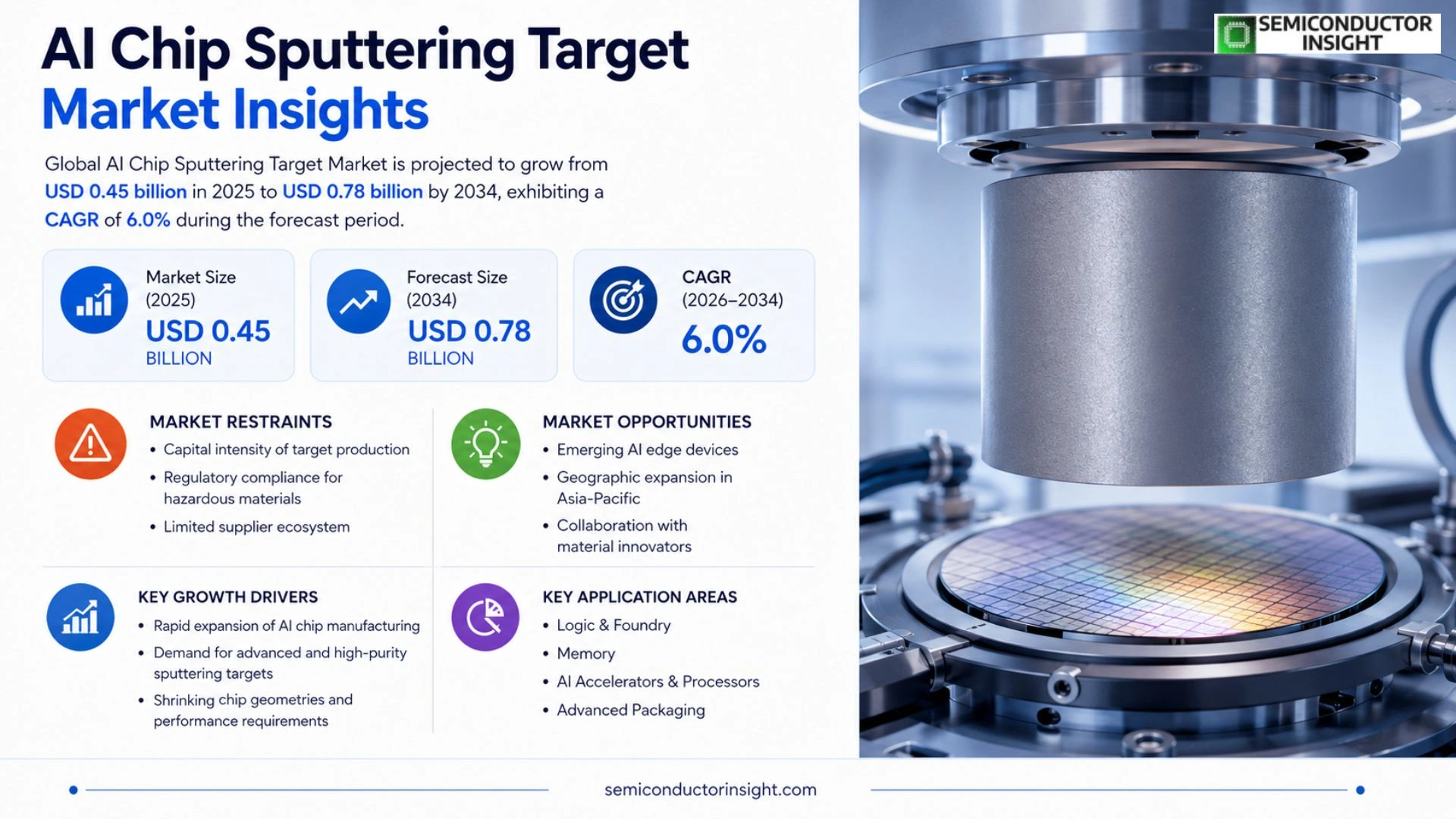
Global AI Chip Sputtering Target Market size was valued at USD 0.45 billion in 2025. The market is projected to grow from USD 0.45 billion in 2025 to USD 0.78 billion by 2034, exhibiting a CAGR of 6.0% during the forecast period.
Sputtering targets for AI chips are high‑purity alloy or compound discs employed in physical vapor deposition chambers to form thin‑film layers on semiconductor wafers. These targets enable precise control of film thickness and composition, which is essential for producing the dense interconnects and advanced nodes required by modern artificial‑intelligence processors.
The market is gaining momentum because AI accelerator demand pushes manufacturers toward finer geometries and higher throughput, prompting fabs to upgrade deposition equipment. Capital commitments from leading foundries and rising adoption of heterogeneous integration further stimulate target consumption. Companies such as Applied Materials, Tokyo Electron and Veeco Instruments have expanded their product portfolios or announced new collaborations aimed at meeting the specific performance criteria of next‑generation AI chips.
MARKET DRIVERS
Rising demand for AI‑optimized processors
The proliferation of generative AI models has forced semiconductor manufacturers to push node sizes below 5 nm. This shift creates a sharp uptick in orders for high‑purity sputtering targets that can sustain the tighter tolerances required by next‑generation AI chips. As fab operators strive to keep cycle times low, any material that improves uniformity directly supports throughput and profitability.
Breakthroughs in sputtering precision
Recent advances in magnetron‑enhanced sputtering have lowered defect densities by as much as 25 % compared with legacy processes. These gains translate into higher yields for AI‑centric wafers, where a single defect can render a high‑value chip unsellable. The technology’s ability to tailor film composition at the atomic level also enables manufacturers to meet the exacting electrical specifications of AI accelerators.
➤ “Precision‑engineered targets reduce wafer defect rates by up to 30 %, delivering measurable cost savings for AI chip fabs.”
When fab capacity constraints intersect with the need for rapid product roll‑outs, the value proposition of specialized sputtering targets becomes a strategic lever. Companies that secure a reliable supply chain can command premium pricing while helping customers accelerate time‑to‑market for AI-enabled silicon.
MARKET CHALLENGES
Technical complexity and yield pressure
Manufacturing sputtering targets that meet sub‑nanometer thickness tolerances demands sophisticated alloy design and tight process control. Any deviation can amplify particle contamination, forcing fabs to reject entire batches and eroding profit margins. This technical burden discourages smaller players from entering the market, concentrating supply among a few established firms.
Other Challenges
Supply‑chain bottlenecks
The scarcity of high‑purity hafnium and titanium, essential for low‑k dielectric layers, creates lead times that often exceed three months. Fab planners must buffer inventory, which inflates working capital and reduces flexibility in responding to sudden demand spikes in AI Chip Sputtering Target Market.
MARKET RESTRAINTS
Capital intensity of target production
Setting up a dedicated sputtering‑target line requires multi‑hundred‑million‑dollar investments in vacuum chambers, plasma sources, and analytical labs. For many mid‑size manufacturers, the upfront cost exceeds the revenue potential of a niche AI wafer segment, leading to under‑investment and slower technology adoption.
Regulatory compliance for hazardous materials
Target alloys often contain cobalt, nickel, or rare‑earth elements that are subject to stringent environmental regulations in Europe and North America. Compliance demands extensive monitoring, waste‑treatment facilities, and periodic audits, adding another layer of operational expense that can deter new entrants.
Limited supplier ecosystem
Only a handful of firms have mastered the end‑to‑end workflow from raw‑material sourcing to final target certification. This concentration risk can lead to price volatility and supply interruptions, especially when geopolitical tensions affect the flow of critical metals.
MARKET OPPORTUNITIES
Emerging AI edge devices
Edge‑computing platforms for autonomous vehicles, smart cameras, and IoT gateways require compact, power‑efficient AI chips. These devices favor sputtering targets that enable ultra‑thin, low‑stress layers, opening a high‑margin niche within the broader AI Chip Sputtering Target Market. Early movers can lock in design‑win partnerships with leading edge‑device manufacturers.
Geographic expansion in Asia‑Pacific
New fab campuses in Taiwan, South Korea, and Japan are scaling up AI‑focused production lines. The regional governments’ incentives for advanced semiconductor ecosystems create a fertile environment for suppliers that can locally source materials and provide rapid target turn‑around.
Collaboration with material innovators
Partnerships between target manufacturers and research institutes are yielding novel alloy compositions that improve thermal conductivity while maintaining electrical isolation. Such co‑development efforts can shorten the time from prototype to volume production, granting participating firms a competitive edge in AI Chip Sputtering Target Market.
AI Chip Sputtering Target Market Trends
Escalating Capital Expenditure Fuels Target Demand
AI Chip Sputtering Target Market is feeling the impact of a pronounced shift in semiconductor investment patterns. In 2023, global capex reached roughly USD 213 billion, and a sizable fraction is now earmarked for advanced packaging and fine‑node processes. Those processes rely on physical vapor deposition, where high‑purity targets dictate film uniformity and electrical performance. Consequently, the market grew from USD 0.85 billion in 2025 to USD 0.92 billion in 2026, and projections place it at USD 1.57 billion by 2034, reflecting a compound annual growth rate of 7.1 percent. The upward trajectory is not merely a function of volume; manufacturers are extracting tighter tolerances from each wafer, prompting more frequent target replacements and a broader material palette. This dynamic reshapes vendor‑buyer negotiations, as buyers press for cost‑effective consistency while suppliers seek to protect margin through process‑specific formulations.
Other Trends
Supply‑Chain Consolidation
Within AI Chip Sputtering Target Market, a handful of established players dominate raw‑material sourcing, target fabrication, and downstream logistics. Recent acquisitions by firms such as Applied have created vertically integrated operations capable of controlling impurity levels from metal ingot to finished disc. This consolidation reduces lead times but also concentrates pricing power, compelling smaller manufacturers to explore strategic partnerships or collaborative R&D to maintain access to premium alloys. Simultaneously, geographic diversification is emerging as a risk‑mitigation tactic; facilities are being positioned nearer to major fabs in Taiwan, South Korea, and the United States to curb transportation delays and align with regional regulatory environments.
Materials Innovation Accelerates Performance Gains
Innovation in target composition is another lever reshaping the market. Researchers are introducing ternary and quaternary compounds that enable sub‑nanometer thickness control, a prerequisite for the high‑frequency transistors powering contemporary neural‑network accelerators. These new materials improve power‑efficiency ratios, which, in turn, lowers thermal budgets for chip designers. For suppliers, the shift demands investment in specialized deposition equipment and tighter quality‑control protocols. From a strategic standpoint, firms that can rapidly qualify novel alloys will capture premium pricing and lock in long‑term supply contracts, while laggards risk being sidelined as fab owners prioritize vendors aligned with next‑generation process nodes.
COMPETITIVE LANDSCAPE
Key Industry Players
Competitive dynamics and positioning in AI chip sputtering targets
Applied Materials continues to dominate the supply chain for high‑purity sputtering targets, leveraging its vertically integrated platform that couples target manufacturing with deposition equipment. The firm’s deep R&D investment in low‑defect, ultra‑thin film processes gives it an advantage when AI‑chip designers demand tighter control over film composition to meet power‑efficiency targets. This leadership forces smaller suppliers to either specialize in niche material chemistries or align with larger OEMs for co‑development projects, shaping a market where scale and technical rigor matter as much as price.
Beyond the flagship player, a cohort of midsize firms is carving out distinct roles. Tokyo Electron and Lam Research provide complementary deposition tools, prompting them to secure exclusive sourcing agreements with target producers such as Veeco Instruments, MKS Instruments, and SPTS Technologies. Meanwhile, regional specialists like Hitachi High‑Tech, Oxford Instruments, and Nanocoatings International focus on specialty compounds—silicon‑germanium alloys, hafnium nitride, and rare‑earth doped targets—serving customers that require unique optical or dielectric characteristics for next‑generation neural‑network accelerators. The fragmentation reinforces a competitive landscape where collaboration and material differentiation drive market share.
List of Key AI Chip Sputtering Target Companies Profiled
- Applied Materials
- Tokyo Electron
- Lam Research
- Veeco Instruments
- MKS Instruments
- SPTS Technologies
- Hitachi High‑Tech
- Oxford Instruments
- Nanocoatings International
- Nanofab Solutions
- Advanced Materials Ltd.
- Precision Target Systems
- Global Sputter Corp.
- Klarfield Technologies
- ASML
Segment Analysis:
| Segment Category | Sub-Segments | Key Insights |
| By Type |
|
Metallic Targets
|
| By Application |
|
AI ASICs
|
| By End User |
|
Semiconductor manufacturers
|
| By Technology |
|
Magnetron Sputtering
|
| By Market Dynamics |
|
Advanced Packaging Integration
|
Regional Analysis: AI Chip Sputtering Target Market
Academic laboratories in Massachusetts and Ontario are co‑authoring patents on alloy compositions that improve target lifespan. Their breakthroughs quickly migrate to commercial fabs, a process reinforced by accelerator‑focused incubators that translate research into production‑ready formulations.
Logistics firms are tailoring cold‑chain services for target pellets, ensuring material integrity from metallurgy workshops to wafer‑fab gates. This alignment trims lead‑times and allows chip makers to schedule sputtering steps tighter within their overall build cycles.
Federal tax credits for clean‑energy manufacturing have been extended to sputtering facilities that adopt renewable power sources, prompting upgrades to electric furnace systems and lowering the carbon profile of the entire value chain.
A handful of AI‑chip designers dominate the North American demand curve, encouraging target producers to develop bespoke alloy mixes that meet highly specific conductivity and thermal‑expansion criteria, fostering a premium‑pricing tier.
Europe
European nations are leveraging their mature semiconductor ecosystems to cultivate a distinct niche in high‑precision sputtering targets. Germany’s engineering culture emphasizes deterministic process control, prompting manufacturers to adopt inline metrology that detects micro‑defects before batch release. The United Kingdom’s focus on sustainable manufacturing has led to pilot projects where recycled metal feedstock is re‑purified for target production, aligning with EU circular‑economy directives. France, meanwhile, benefits from cross‑border research consortia that blend materials science with AI‑driven design optimization, delivering alloy recipes that balance hardness with electron‑emission efficiency. Collectively, these dynamics nurture an environment where European firms can command higher margins by offering differentiated performance guarantees to AI‑chip OEMs seeking regulatory‑compliant supply options.
Asia‑Pacific
In the Asia‑Pacific corridor, rapid capacity expansion is coupled with an escalating emphasis on cost efficiency. China’s sprawling fab clusters have spurred a competitive market for low‑cost sputtering targets, driving manufacturers to scale up bulk‑melting operations while maintaining tight compositional tolerances through AI‑guided process analytics. South Korea’s semiconductor giants are integrating sputtering target design directly into their chip architecture teams, shortening feedback loops and enabling faster iteration on device‑specific material requirements. Japan, with its legacy of precision metalworking, continues to supply ultra‑pure targets for niche AI applications such as edge inference processors, where defect density directly impacts yield. The region’s blend of volume, precision, and emerging AI‑driven process control creates a versatile supply base that can adapt to varying price‑performance trade‑offs demanded by global customers.
South America
South America remains an emerging participant, with Brazil leading efforts to diversify its semiconductor supply chain beyond traditional imports. Government‑backed research hubs are experimenting with locally sourced copper‑based alloys, aiming to reduce reliance on Asian imports while meeting the purity benchmarks required for AI‑chip sputtering. Argentina’s academic institutions contribute by modeling plasma‑target interactions, offering insights that help regional players tune deposition parameters for specific AI workloads. Although scale is modest, the focus on domestic material development and collaborative research positions the continent as a potential alternative source of specialty targets for manufacturers looking to mitigate geopolitical risk.
Middle East & Africa
The Middle East & Africa region is at an exploratory stage, with United Arab Emirates and South Africa establishing pilot lines that combine renewable energy generation with target fabrication. The UAE’s investment in solar‑powered metallurgical plants reflects a strategy to align high‑tech manufacturing with sustainability goals, while South Africa leverages its mineral wealth to produce base metal feedstock for target alloys. Early‑stage collaborations between local universities and multinational equipment suppliers are generating proof‑of‑concept studies that demonstrate feasibility of cost‑effective, low‑emission sputtering processes. Though still nascent, these initiatives lay the groundwork for a geographically diversified supply network that could serve niche segments of AI Chip Sputtering Target Market.
Report Scope
This market research report provides a comprehensive analysis of the AI Chip Sputtering Target Market , covering the forecast period 2026–2034. It offers detailed insights into market dynamics, technological advancements, competitive landscape, and key trends shaping the industry.
Key focus areas of the report include:
- Market Overview: The report begins with an overview outlining its current market scenario, key growth indicators, and industry transformation drivers. It discusses macroeconomic factors, demand–supply balance, regulatory landscape, and the strategic role of semiconductors in powering advancements across industries such as automotive, telecommunications, consumer electronics, and industrial automation.
- Market Size & Forecast: Historical data and future projections for revenue, unit shipments, and market value across major regions and segments.
- Segmentation Analysis: Detailed breakdown by product type, technology, application, and end-user industry to identify high-growth segments and investment opportunities.
- Regional Insights: Insights into market performance across North America, Europe, Asia-Pacific, Latin America, and the Middle East & Africa, including country-level analysis where relevant.
- Competitive Landscape: Profiles of leading market participants, including their product offerings, R&D focus, manufacturing capacity, pricing strategies, and recent developments such as mergers, acquisitions, and partnerships.
- Technology Trends & Innovation: Assessment of emerging technologies, integration of AI/IoT, semiconductor design trends, fabrication techniques, and evolving industry standards.
- Market Drivers & Restraints: Evaluation of factors driving market growth along with challenges, supply chain constraints, regulatory issues, and market-entry barriers.
- Stakeholder Insights: Insights for component suppliers, OEMs, system integrators, investors, and policymakers regarding the evolving ecosystem and strategic opportunities.
Primary and secondary research methods are employed, including interviews with industry experts, data from verified sources, and real-time market intelligence to ensure the accuracy and reliability of the insights presented.
FREQUENTLY ASKED QUESTIONS:
What is the current market size of AI Chip Sputtering Target Market?
-> AI Chip Sputtering Target Market was valued at USD 0.85 billion in 2025 and is expected to reach USD 1.57 billion by 2034, reflecting a CAGR of 7.1% over the forecast period.
Which key companies operate in AI Chip Sputtering Target Market?
-> Key players include Applied Materials, Lam Research, Tokyo Electron, Hitachi High‑Technologies, and ASM International, among others.
What are the key growth drivers?
-> Key growth drivers include rising demand for AI‑optimized chips, increasing semiconductor capital expenditure, adoption of advanced packaging techniques, and the need for high‑purity sputtering targets to support finer node technologies.
Which region dominates the market?
-> Asia‑Pacific dominates the market owing to its extensive semiconductor manufacturing base, while Europe remains a significant contributor.
What are the emerging trends?
-> Emerging trends include development of composite and nano‑structured targets, integration of AI‑driven process control, and sustainability initiatives targeting reduced material waste.

Get Sample Report PDF for Exclusive Insights
Report Sample Includes
- Table of Contents
- List of Tables & Figures
- Charts, Research Methodology, and more...
 Download Sample Report PDF