
AI Chip Package Warpage Simulation and Metrology Market Insights
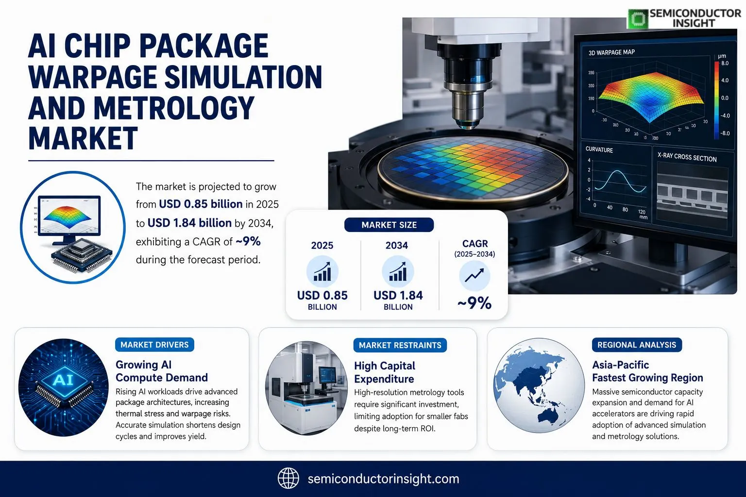
AI chip package warpage simulation and metrology market size was valued at USD 0.78 billion in 2025.The market is projected to grow from USD 0.85 billion in 2025 to USD 1‑84 billion by 2034, exhibiting a CAGR of ~9% during the forecast period.
AI chip package warpage simulation refers to computational modeling techniques that predict out‑of‑plane deformation of advanced heterogeneous packages under thermal‑mechanical loads.Metrology encompasses high‑precision measurement solutionssuch as laser interferometry, atomic force microscopy, and X‑ray imagingused to quantify wafer‑level curvature, die‑level bow, and stack‑up alignment after bonding.Together these capabilities enable designers to optimize material stacks, mitigate reliability risks, and accelerate time‑to‑market for high‑performance AI accelerators.The market is experiencing rapid expansion because AI workloads demand ever‑denser interconnects and heterogeneous integration, which intensify warpage challenges.Furthermore, the shift toward fan‑out wafer‑level packaging (FOWLP) and silicon interposers drives adoption of predictive simulation tools that reduce costly silicon rework.The rise of edge computing devices also pushes manufacturers toward tighter tolerances measured by next‑generation metrology platforms.Key players such as Synopsys, Cadence Design Systems, Ansys, KLA‑Tencor, Nikon Metrology are expanding their portfolios through strategic acquisitions and joint development programs aimed at delivering integrated design‑for‑manufacturability solutions.
MARKET DRIVERS
Growing AI Compute Demand
The surge in AI workloads is compelling semiconductor manufacturers to adopt advanced package architectures. These architectures generate higher thermal gradients, which increase the risk of warpage and jeopardize product yield. Companies that invest in accurate warpage simulation can shorten time‑to‑market by identifying stress points early in the design cycle.
Advances in Simulation Software
Recent enhancements in finite‑element modelling and machine‑learning‑assisted predictive tools enable sub‑micron accuracy for package deformation forecasts. This capability translates into reduced reliance on costly physical prototypes and lower overall development spend.
➤ Industry surveys indicate that firms employing integrated simulation and metrology reduce prototype iterations by up to 30 %.
As AI edge devices proliferate, the need for reliable, high‑density interconnects intensifies, making warpage control a strategic priority for AI Chip Package Warpage Simulation and Metrology Market.
MARKET CHALLENGES
Complex Multilayer Stack Designs
AI chips are increasingly built on heterogeneous stacks that combine silicon, silicon‑on‑insulator, and advanced interposers. The differing coefficients of thermal expansion create non‑linear warpage patterns that are difficult to predict with conventional tools.
Other Challenges
Tool Integration Issues
Legacy design‑automation environments often lack seamless interfaces with the latest metrology platforms, forcing engineers to perform manual data translation that can introduce errors and delay decision‑making.
MARKET RESTRAINTS
High Capital Expenditure
The acquisition cost of high‑resolution metrology equipment, such as interferometric profilers and 3‑D X‑ray scanners, remains a deterrent for smaller fabs. While the return on investment materializes over several product cycles, the upfront spend can limit market participation and slow broader adoption.
MARKET OPPORTUNITIES
Emerging 3D‑Stacked AI Packages
Three‑dimensional integration promises unprecedented compute density for AI accelerators. However, the tightly coupled layers magnify warpage sensitivities, creating a clear demand for next‑generation simulation algorithms and real‑time metrology feedback loops. Vendors that can deliver scalable, AI‑driven analytics are poised to capture a significant share of the evolving market.
AI Chip Package Warpage Simulation and Metrology Market Trends
Accelerated Adoption Driven by AI Workloads and Heterogeneous Integration
AI Chip Package Warpage Simulation and Metrology Market is expanding as designers confront the thermal‑mechanical stresses that accompany AI‑centric silicon interposers and dense 3‑D stacking. AI accelerators require higher pin counts and tighter pitch, which magnify out‑of‑plane deformation during molding, bonding, and thermal cycling. Predictive simulation tools now enable engineers to model these deformations early in the design cycle, reducing costly silicon rework and shortening time‑to‑market. Leading EDA vendors such as Synopsys, Cadence Design Systems, and Ansys are integrating warpage solvers into their design suites, while metrology specialists including KLA‑Tencor and Nikon Metrology are bundling high‑resolution measurement modules with simulation data flows. The combined effect is a more robust design‑for‑manufacturability workflow that aligns with the performance expectations of next‑generation AI chips.
Other Trends
Emergence of Fan‑Out Wafer‑Level Packaging (FOWLP)
Fan‑Out Wafer‑Level Packaging is reshaping the warpage landscape because it removes the traditional substrate and relies on redistributive layers that are highly susceptible to curvature changes. As manufacturers shift to FOWLP for AI chips, simulation accuracy becomes critical to predict wafer‑level bow before dicing. The market response includes tighter integration between simulation platforms and process‑monitoring tools, allowing rapid iteration of material stack selections. Early‑stage virtual trials lower the incidence of post‑bond rework, delivering measurable yield improvements while supporting the aggressive form‑factor targets of edge‑AI devices.
Metrology Advancements Enabling Tight Tolerances
Metrology solutions are evolving to keep pace with the sub‑micron tolerances demanded by AI chip packages. Laser interferometry now offers nanometer‑scale curvature mapping across entire wafers, while atomic force microscopy provides localized die‑level bow measurements that feed directly into simulation refinement loops. X‑ray imaging adds depth insight for stacked interposers, completing a holistic metrology suite. These capabilities allow manufacturers to verify that simulated warpage predictions align with actual physical outcomes, thereby reducing risk and supporting the rapid deployment cycles of AI accelerators. Strategic collaborations among the key players are accelerating the rollout of integrated simulation‑metrology platforms, reinforcing the market’s trajectory toward higher reliability and faster product introductions.
COMPETITIVE LANDSCAPE
Key Industry Players
AI Chip Package Warpage Simulation and Metrology Market – Competitive Overview
AI Chip Package Warpage Simulation and Metrology Market is currently led by a handful of software and instrumentation giants that command the majority of revenue. Synopsys, with its extensive suite of simulation tools, partners closely with foundries to embed predictive warpage models into the design flow. Cadence Design Systems leverages its Virtuoso and Tempus platforms to offer integrated thermal‑mechanical analysis, while ANSYS provides high‑fidelity multiphysics solvers that address the complex stack‑up interactions of heterogeneous AI packages. On the metrology side, KLA‑Tencor’s advanced wafer‑level curvature sensors and Nikon Metrology’s X‑ray imaging systems have become de‑facto standards for in‑process verification. The convergence of these capabilities under unified design‑for‑manufacturability (DFM) solutions has reinforced a market structure in which the top five participants capture roughly 60 % of total spend, driving a competitive dynamic centered on portfolio breadth, accuracy, and ecosystem partnerships.Beyond the dominant players, a diverse set of niche specialists contributes depth and innovation to the ecosystem. Applied Materials and Lam Research extend their lithography‑adjacent metrology offerings to include laser interferometry and post‑bond bow measurement, targeting mid‑size fab customers. ASM International and Tokyo Electron focus on material‑level tools that support silicon interposer and fan‑out wafer‑level packaging (FOWLP) processes. Intel’s internal packaging engineering team and TSMC’s Advanced Packaging division have developed proprietary simulation kernels to optimize AI accelerator stacks, often collaborating with the larger EDA vendors. ASE Technology Holding and Samsung Electro‑Mechanics provide turnkey packaging services that integrate third‑party simulation data with on‑site metrology, while Foundries and STMicroelectronics maintain in‑house capabilities to support niche AI workloads. Collectively, these players enhance market resilience by addressing specific technology nodes, regional demand, and emerging form‑factors such as edge AI devices.
List of Key AI Chip Package Warpage Simulation and Metrology Companies Profiled
- Synopsys, Inc.
- Cadence Design Systems, Inc.
- ANSYS, Inc.
- KLA‑Tencor Corporation
- Nikon Metrology
- Applied Materials, Inc.
- Lam Research Corporation
- ASM International N.V.
- Tokyo Electron Limited
- Intel Corporation
- TSMC – Advanced Packaging Division
- ASE Technology Holding Co., Ltd.
- Samsung Electro‑Mechanics
- Foundries
- STMicroelectronics
Segment Analysis:
| Segment Category | Sub-Segments | Key Insights |
| By Type |
|
Simulation Software Platforms dominate the early design ecosystem, enabling engineers to anticipate warp behavior before physical prototypes exist. They are valued for:
|
| By Application |
|
High‑Performance AI Accelerators drive demand for precise warpage control due to dense interconnects and 3‑D stacking. Key qualitative factors include:
|
| By End User |
|
Chip Design Houses are the primary adopters of warpage simulation because they embed reliability checks directly into architecture decisions. Their qualitative drivers include:
|
| By Technology |
|
Machine‑Learning‑Enhanced Predictive Models are gaining traction as they fuse data‑driven insights with physics‑based simulation, offering nuanced warp forecasts. Notable qualitative benefits:
|
| By Deployment Stage |
|
Prototype Validation emerges as the pivotal stage where simulation outcomes are cross‑checked with high‑resolution metrology, shaping final product readiness. Qualitative considerations include:
|
Regional Analysis: AI Chip Package Warpage Simulation and Metrology Market
North America
The region’s fabs are integrating multi‑physics simulation workflows that couple thermal, mechanical, and electrical analyses. This holistic approach shortens design validation, reduces re‑work, and aligns with the aggressive volume targets set by leading OEMs in AI‑driven data centers.
Established vendors such as Cadence, Synopsys, and KLA dominate, while emerging startups bring AI‑optimized algorithms that automate defect detection and warpage prediction, intensifying competitive dynamics.
Cloud‑based simulation services are gaining traction, allowing smaller packaging firms to access high‑performance compute resources without large capital outlays, accelerating overall market diffusion.
IEEE and JEDEC standards are being updated to incorporate tighter warpage tolerance metrics, guiding both design engineers and metrology providers toward consistent quality benchmarks.
Europe
Europe’s AI Chip Package Warpage Simulation and Metrology market is characterized by a strong emphasis on collaborative research programs funded by the EU Horizon initiatives. Major automotive and industrial chip makers are driving demand for precise warpage control in power electronics, prompting manufacturers to adopt high‑resolution optical and X‑ray metrology tools. While the region lags slightly behind North America in pure‑play AI‑enhanced simulation software, partnerships between semiconductor equipment firms and academic institutions are accelerating technology transfer. Regulatory bodies are actively harmonizing standards across member states, which helps streamline cross‑border supply chains and reduces time‑to‑market for advanced packaging solutions.
Asia‑Pacific
The Asia‑Pacific region exhibits the fastest growth trajectory, propelled by massive capacity expansions in Taiwan, South Korea, and China. These countries are scaling up advanced packaging lines for AI accelerators, where warpage control is critical to maintaining performance at high frequencies. Local equipment manufacturers are embedding AI‑driven analytics directly into metrology platforms, offering real‑time feedback during wafer processing. Although cost considerations drive a preference for lower‑cost simulation tools, the competitive pressure to achieve leading‑edge chip densities encourages rapid adoption of sophisticated predictive models. Trade policies and export controls occasionally affect technology flow, but regional trade agreements continue to support a vibrant ecosystem.
South America
South America remains a developing market for AI Chip Package Warpage Simulation and Metrology, with Brazil leading modest adoption in niche high‑performance computing projects. Local semiconductor ventures are focusing on pilot lines that test AI‑enhanced simulation workflows, often relying on partnerships with North American and European vendors for software licensing. The limited domestic manufacturing base constrains large‑scale deployment, yet growing interest in autonomous vehicle electronics and renewable‑energy power modules fuels incremental demand for precise warpage monitoring. Government incentives aimed at technology transfer are beginning to stimulate modest investments in metrology infrastructure.
Middle East & Africa
In the Middle East & Africa, market activity is primarily driven by strategic investments in smart‑city and defense electronics that require reliable AI chip packaging. Region‑specific initiatives in the United Arab Emirates and South Africa are establishing test labs equipped with advanced metrology equipment supplied by OEMs. Although the overall market size is small, early adopters are leveraging cloud‑based simulation services to offset limited local expertise. Ongoing collaborations with international research institutes are expected to nurture a skilled talent pool, laying groundwork for more widespread usage of warpage simulation and metrology solutions in the coming years.
Report Scope
This market research report provides a comprehensive analysis of the AI Chip Package Warpage Simulation and Metrology Market , covering the forecast period 2026–2034. It offers detailed insights into market dynamics, technological advancements, competitive landscape, and key trends shaping the industry.
Key focus areas of the report include:
- Market Overview: The report begins with an overview outlining its current market scenario, key growth indicators, and industry transformation drivers. It discusses macroeconomic factors, demand–supply balance, regulatory landscape, and the strategic role of semiconductors in powering advancements across industries such as automotive, telecommunications, consumer electronics, and industrial automation.
- Market Size & Forecast: Historical data and future projections for revenue, unit shipments, and market value across major regions and segments.
- Segmentation Analysis: Detailed breakdown by product type, technology, application, and end-user industry to identify high-growth segments and investment opportunities.
- Regional Insights: Insights into market performance across North America, Europe, Asia-Pacific, Latin America, and the Middle East & Africa, including country-level analysis where relevant.
- Competitive Landscape: Profiles of leading market participants, including their product offerings, R&D focus, manufacturing capacity, pricing strategies, and recent developments such as mergers, acquisitions, and partnerships.
- Technology Trends & Innovation: Assessment of emerging technologies, integration of AI/IoT, semiconductor design trends, fabrication techniques, and evolving industry standards.
- Market Drivers & Restraints: Evaluation of factors driving market growth along with challenges, supply chain constraints, regulatory issues, and market-entry barriers.
- Stakeholder Insights: Insights for component suppliers, OEMs, system integrators, investors, and policymakers regarding the evolving ecosystem and strategic opportunities.
Primary and secondary research methods are employed, including interviews with industry experts, data from verified sources, and real-time market intelligence to ensure the accuracy and reliability of the insights presented.
FREQUENTLY ASKED QUESTIONS:
What is the current market size of AI Chip Package Warpage Simulation and Metrology Market?
-> AI Chip Package Warpage Simulation and Metrology Market was valued at USD 0.78 billion in 2025 and is expected to reach USD 1.84 billion by 2034, representing a CAGR of ~9% over the forecast period.
Which key companies operate in AI Chip Package Warpage Simulation and Metrology Market?
-> Key players include Synopsys, Cadence Design Systems, Ansys, KLA‑Tencor, Nikon Metrology, among others.
What are the key growth drivers?
-> Growth is driven by increasing AI workloads demanding denser interconnects, the shift toward fan‑out wafer‑level packaging (FOWLP), and rising edge‑computing applications that require tighter warpage tolerances and advanced metrology.
Which region dominates the market?
-> Asia‑Pacific is the fastest‑growing region, while North America remains a dominant market due to strong semiconductor R&D and early adopter ecosystem.
What are the emerging trends?
-> Emerging trends include AI‑enhanced predictive simulation, high‑resolution laser interferometry and X‑ray metrology platforms, and integrated design‑for‑manufacturability solutions that combine simulation and metrology in a unified workflow.
Get Sample Report PDF for Exclusive Insights
Report Sample Includes
- Table of Contents
- List of Tables & Figures
- Charts, Research Methodology, and more...





