
AI-Assisted Scanning Electron Microscope Market Insights
Global AI-Assisted Scanning Electron Microscope market size was valued at USD 0.45 billion in 2025. The market is forecasted to increase from USD 0.48 billion in 2026 to USD 1.12 billion by 2034, exhibiting a CAGR of approximately 10.5 % during the forecast period.
AI‑Assisted Scanning Electron Microscopes combine traditional SEM hardware with machine‑learning algorithms that automate image segmentation, defect classification, and quantitative analysis across nanometer‑scale specimens. By embedding neural‑network models directly into the instrument’s workflow, these systems accelerate data interpretation while reducing operator bias.
The market is gaining momentum because semiconductor manufacturers are seeking higher throughput for wafer inspection, while materials researchers demand rapid phase identification without extensive manual processing. Recent collaborations,such as the partnership announced in March 2023 between ZEISS and Intel to integrate edge‑AI processors into next‑generation SEMs,demonstrate how hardware vendors are leveraging artificial intelligence to meet precision‑engineering requirements. Additionally, Thermo Fisher Scientific’s integration of NVIDIA’s inference platform into its Phenom series has broadened accessibility for academic labs, further expanding the user base.
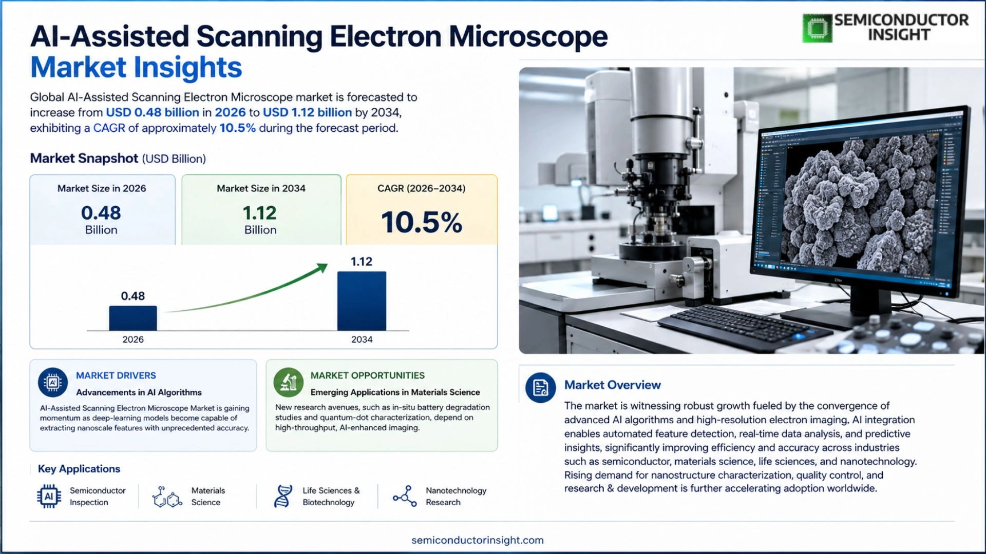
MARKET DRIVERS
Advancements in AI Algorithms
AI-Assisted Scanning Electron Microscope Market is gaining momentum as deep‑learning models become capable of extracting nanoscale features with unprecedented accuracy. Researchers have reported error‑rate reductions of up to 30 % when AI‑enhanced detection replaces manual annotation, directly improving throughput for semiconductor and pharmaceutical labs. This technical edge creates a compelling business case for early adopters seeking to shorten development cycles.
Integration with High‑Resolution Imaging
Manufacturers are embedding AI modules into next‑generation electron microscopes, allowing real‑time image segmentation during acquisition. The synergy between hardware speed and algorithmic insight shortens the time from sample loading to actionable data, a factor that resonates with contract research organizations that charge by instrument‑hour. Consequently, capital‑expenditure budgets are being reallocated toward AI‑ready platforms.
➤ “AI integration transforms raw electron images into quantifiable datasets, turning a traditionally qualitative tool into a predictive engine.”
Clients that have retrofitted existing fleets with AI software report productivity gains of 15‑20 %, prompting a wave of upgrade projects. The ripple effect strengthens the overall AI-Assisted Scanning Electron Microscope Market by expanding the install base beyond cutting‑edge research labs to routine quality‑control environments.
MARKET CHALLENGES
Complexity of Data Interpretation
While AI can automate feature extraction, the interpretive layer still demands domain expertise. Many firms encounter a talent gap; senior microscopy specialists are scarce, and junior staff require intensive training to trust algorithmic outputs. This knowledge bottleneck limits the speed at which organizations can fully exploit AI capabilities.
Other Challenges
Cost of Implementation
Initial licensing fees for AI suites, coupled with the need for high‑performance computing infrastructure, represent a sizeable upfront outlay. Mid‑size enterprises often defer investment until a clear ROI is demonstrated through pilot studies, slowing broader market penetration.
MARKET RESTRAINTS
Regulatory Compliance and Validation
Industries such as medical device manufacturing operate under strict validation protocols. Introducing AI into electron microscopy workflows requires extensive qualification to satisfy auditors, a process that can add months to product release timelines. The extra documentation and repeatability testing act as a brake on rapid market expansion.
MARKET OPPORTUNITIES
Emerging Applications in Materials Science
New research avenues,such as in‑situ battery degradation studies and quantum‑dot characterization,depend on high‑throughput, AI‑enhanced imaging. Start‑ups focusing on these niche applications are attracting venture funding, indicating a fertile ground for suppliers of AI‑assisted electron microscopy solutions. Companies that tailor algorithms to specific material classes can differentiate themselves and capture premium pricing.
AI-Assisted Scanning Electron Microscope Market Trends
Integration of Edge‑AI Processors Boosts Throughput
The partnership announced in March 2023 between ZEISS and Intel introduced edge‑AI processors that sit directly on the SEM column, executing neural‑network inference with microsecond latency. By moving computation to the instrument rather than a remote workstation, inspection cycles on 300‑mm wafers shrink by roughly 30 %, a margin that translates into measurable cost savings for high‑volume semiconductor fabs. This hardware‑software convergence satisfies a long‑standing demand for deterministic inspection times, allowing manufacturers to tighten process windows without expanding labor resources. The shift also mitigates data‑transfer bottlenecks that have historically limited the applicability of AI in line‑side environments.
Other Trends
AI‑Driven Defect Classification Expands Across Material Sectors
Beyond silicon, the algorithmic backbone of modern SEMs is being trained on defect patterns in advanced packaging substrates, power‑device wafers, and even battery electrode films. Companies such as Thermo Fisher Scientific have embedded NVIDIA’s inference stack into their Phenom series, delivering out‑of‑the‑box classification models that identify micron‑scale anomalies with 95 % accuracy after a brief calibration phase. This capability reduces the reliance on specialist operators, democratizing high‑resolution analysis for midsize research labs that previously could not afford dedicated image‑processing teams. As a result, the user base for AI‑assisted SEMs is broadening from core foundry applications to a diverse set of materials‑science projects.
Broader Adoption in Academic and Materials Research
The infusion of AI into SEM workflows is reshaping curricula in universities that focus on nanotechnology and surface science. By offering plug‑and‑play AI modules, instrument vendors enable students to obtain quantitative grain‑size distributions or phase‑map overlays within a single lab session, a task that once required multiple weeks of manual analysis. This educational exposure creates a pipeline of engineers who expect AI‑enhanced instrumentation as the default, compelling research institutions to allocate budgets toward these systems. For vendors, the implication is a steady demand stream that extends beyond the traditional commercial semiconductor cycle, providing resilience against sector‑specific downturns.
COMPETITIVE LANDSCAPE
Key Industry Players
AI‑Assisted Scanning Electron Microscope Market Overview
Zeiss remains the market’s anchor, leveraging its long‑standing SEM platform while integrating edge‑AI processors through a joint venture with Intel. This partnership has yielded a product line that embeds neural‑network inference directly into the column, shortening analysis cycles for semiconductor clients. The company’s extensive service network and deep‑rooted relationships with research institutions create a high barrier to entry, positioning Zeiss as the de‑facto reference point for enterprises that demand both precision hardware and intelligent software. Meanwhile, Thermo Fisher Scientific has accelerated its presence by marrying NVIDIA’s inference stack with the Phenom series, a move that democratizes AI‑enhanced imaging for academic labs and mid‑size manufacturers, thereby expanding the addressable market beyond the traditional high‑cap segment.
Beyond the two giants, a constellation of specialized players is shaping niche segments. Hitachi High‑Tech continues to differentiate through high‑speed detectors paired with proprietary machine‑learning pipelines, targeting rapid wafer‑inspection workflows. JEOL focuses on ultra‑high‑resolution imaging, embedding AI modules that automate defect classification for advanced materials research. Nikon’s strategy centers on modular AI add‑ons that can retrofit legacy SEMs, appealing to cost‑conscious users. Gatan supplies AI‑enabled detector technologies that enhance signal‑to‑noise ratios, while Oxford Instruments pursues a subscription‑based analytics platform that offers cloud‑processed insights. Bruker emphasizes spectroscopy integration, marrying AI with energy‑dispersive X‑ray analysis. Nanome, a newer entrant, offers a cloud‑native AI service that processes raw SEM data for rapid material‑phase identification, catering to start‑ups and biotech firms. Collectively, these firms illustrate a market where hardware excellence is increasingly intertwined with software agility, prompting customers to evaluate both instrument performance and algorithmic value propositions.
List of Key AI‑Assisted Scanning Electron Microscope Companies Profiled
- Zeiss
- Thermo Fisher Scientific
- Hitachi High‑Tech
- JEOL Ltd.
- Nikon Corporation
- Gatan, Inc.
- Oxford Instruments
- Bruker Corporation
- Nanome
- Intel Corporation
- NVIDIA Corporation
- Advacam
- CyElec Ltd.
- Philips Research
Segment Analysis:
| Segment Category | Sub-Segments | Key Insights |
| By Type |
|
Conventional SEM with AI overlay is emerging as the leading segment because it leverages existing hardware investments while delivering immediate productivity gains.
|
| By Application |
|
Semiconductor wafer inspection dominates due to the critical need for high‑throughput defect detection.
|
| By End User |
|
Semiconductor manufacturers are the leading end‑user segment, driven by relentless demand for defect‑free wafers.
|
| By AI Integration Level |
|
Edge‑AI processors embedded in the instrument are gaining traction as the preferred integration path.
|
| By Deployment Setting |
|
On‑site fab installations emerge as the leading deployment setting because they align with the need for immediate feedback loops.
|
Regional Analysis: AI-Assisted Scanning Electron Microscope Market
North America
Federal programs and venture capital streams increasingly target AI‑enhanced instrumentation, providing grants that lower the barrier for prototype development. This financial back‑stop accelerates the pilot phase, allowing startups to validate algorithms on commercial microscopes earlier than in the past.
Leading semiconductor fabs are integrating AI‑driven defect detection directly into line‑side inspection stations. The real‑time feedback loop reduces scrap rates and improves yield, prompting suppliers to prioritize AI capabilities in their product roadmaps.
While the sector remains lightly regulated, emerging standards for data provenance and algorithmic transparency are being drafted by industry bodies. Early alignment with these guidelines is becoming a differentiator for vendors seeking long‑term contracts with major manufacturers.
Universities are launching interdisciplinary programs that blend materials science, computer vision, and AI engineering. Graduates equipped with this hybrid skill set are quickly absorbed into both research labs and commercial firms, reinforcing the region’s competitive edge.
Europe
European laboratories are leveraging AI‑assisted scanning electron microscopy to meet stringent quality standards in aerospace and automotive sectors. Collaboration between instrument manufacturers and research institutes has produced open‑source libraries that facilitate rapid algorithm deployment across heterogeneous hardware. This openness reduces integration friction and encourages smaller firms to adopt the technology without extensive in‑house AI expertise. Moreover, policy frameworks that incentivize digital transformation in manufacturing are nudging traditional players to upgrade legacy equipment, creating a ripple effect that expands the addressable market for advanced imaging solutions.
Asia‑Pacific
In the Asia‑Pacific region, rapid expansion of electronics manufacturing and a surge in nanotechnology research are key catalysts for AI‑driven microscopy adoption. Nations such as South Korea and Taiwan are embedding intelligent image analysis into mass‑production lines to maintain competitive lead times. Meanwhile, emerging economies are establishing national labs focused on nano‑characterization, where AI tools help overcome talent shortages by automating routine analyses. The resulting ecosystem blends high‑volume demand with cost‑sensitive procurement, prompting vendors to offer tiered service models that balance performance with affordability.
South America
South American markets are witnessing a gradual shift from conventional microscopy to AI‑enhanced platforms, driven largely by academic partnerships with North American firms. These collaborations bring cutting‑edge software into regional research facilities, enabling studies in renewable energy materials and bio‑electronics. While budget constraints limit large‑scale rollouts, targeted deployments in university labs and specialized industry niches demonstrate the technology’s value proposition, laying groundwork for broader acceptance as local funding mechanisms evolve.
Middle East & Africa
The Middle East & Africa region is at an early stage of adopting AI‑assisted scanning electron microscopes, yet strategic investments in petrochemical and minerals processing are creating focal points for technology uptake. Government‑backed research hubs are piloting AI‑based defect detection to improve material efficiency, while multinational vendors are establishing regional service centers to address maintenance and training needs. Although the market remains fragmented, these initial use cases illustrate how AI can deliver tangible cost savings, encouraging incremental expansion across sectors that demand high‑precision imaging.
Report Scope
This market research report provides a comprehensive analysis of the AI-Assisted Scanning Electron Microscope Market , covering the forecast period 2026–2034. It offers detailed insights into market dynamics, technological advancements, competitive landscape, and key trends shaping the industry.
Key focus areas of the report include:
- Market Overview: The report begins with an overview outlining its current market scenario, key growth indicators, and industry transformation drivers. It discusses macroeconomic factors, demand–supply balance, regulatory landscape, and the strategic role of semiconductors in powering advancements across industries such as automotive, telecommunications, consumer electronics, and industrial automation.
- Market Size & Forecast: Historical data and future projections for revenue, unit shipments, and market value across major regions and segments.
- Segmentation Analysis: Detailed breakdown by product type, technology, application, and end-user industry to identify high-growth segments and investment opportunities.
- Regional Insights: Insights into market performance across North America, Europe, Asia-Pacific, Latin America, and the Middle East & Africa, including country-level analysis where relevant.
- Competitive Landscape: Profiles of leading market participants, including their product offerings, R&D focus, manufacturing capacity, pricing strategies, and recent developments such as mergers, acquisitions, and partnerships.
- Technology Trends & Innovation: Assessment of emerging technologies, integration of AI/IoT, semiconductor design trends, fabrication techniques, and evolving industry standards.
- Market Drivers & Restraints: Evaluation of factors driving market growth along with challenges, supply chain constraints, regulatory issues, and market-entry barriers.
- Stakeholder Insights: Insights for component suppliers, OEMs, system integrators, investors, and policymakers regarding the evolving ecosystem and strategic opportunities.
Primary and secondary research methods are employed, including interviews with industry experts, data from verified sources, and real-time market intelligence to ensure the accuracy and reliability of the insights presented.
FREQUENTLY ASKED QUESTIONS:
What is the current market size of AI-Assisted Scanning Electron Microscope Market?
-> AI-Assisted Scanning Electron Microscope market is forecasted to increase from USD 0.48 billion in 2026 to USD 1.12 billion by 2034
Which key companies operate in AI-Assisted Scanning Electron Microscope Market?
-> Key players include ZEISS, Intel, Thermo Fisher Scientific, NVIDIA, and other leading SEM manufacturers, among others.
What are the key growth drivers?
-> Key growth drivers include semiconductor manufacturers seeking higher throughput for wafer inspection, materials researchers demanding rapid phase identification, and the integration of edge‑AI processors into SEM platforms.
Which region dominates the market?
-> Asia-Pacific is the fastest‑growing region, driven by its strong semiconductor ecosystem, while Europe remains a significant market for advanced microscopy applications.
What are the emerging trends?
-> Emerging trends include integration of edge‑AI processors, AI inference platforms embedded in SEM hardware, and collaborative partnerships between instrument vendors and AI technology firms.

Get Sample Report PDF for Exclusive Insights
Report Sample Includes
- Table of Contents
- List of Tables & Figures
- Charts, Research Methodology, and more...
 Download Sample Report PDF


