2 inch Patterned Sapphire Substrates Market Insights
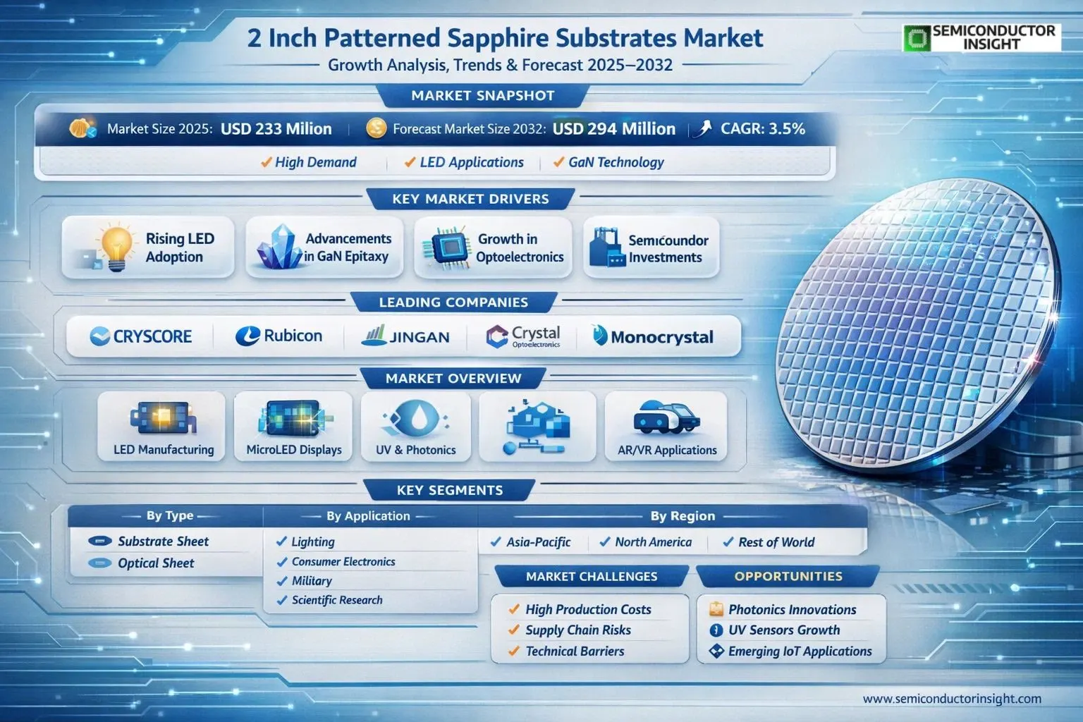
Global 2 inch Patterned Sapphire Substrates market size was valued at USD 233 million in 2025. The market is projected to reach USD 294 million by 2032, exhibiting a CAGR of 3.5% during the forecast period.
Patterned Sapphire Substrates are key materials used in the manufacture of high-brightness LED chips. Primarily composed of aluminum oxide (Al2O3), they offer exceptional properties including high acoustic velocity, temperature resistance, corrosion resistance, hardness, and light transmittance. As single-crystal wafers, they enable epitaxial growth of crystalline thin films, allowing semiconductors like gallium nitride (GaN) to grow directionally and produce superior LED chips.
The market is experiencing steady growth driven by rising demand for efficient LEDs in lighting and displays, advancements in GaN-based technologies, and expansion in optoelectronics. Furthermore, increasing investments in semiconductor manufacturing bolster this trajectory. Key players such as CRYSCORE, Rubicon Technology, Jingan Optoelectronics, Jiaxing Jingdian, Crystal Optoelectronics, Bright Semiconductor, Qingdao Huaxin Wafer Technology, and Monocrystal dominate with significant revenue shares, focusing on innovation and capacity expansion to meet global needs.
MARKET DRIVERS
Advancements in LED Light Extraction Efficiency
2 inch Patterned Sapphire Substrates Market is propelled by innovations in GaN-on-sapphire epitaxy, where patterned structures enhance external quantum efficiency by up to 30% compared to planar substrates. This drives adoption in high-performance blue and green LED production, critical for next-generation displays and lighting solutions.
Growth in MicroLED and Optoelectronics Demand
Rising applications in microLED displays for consumer electronics, including AR/VR devices, boost demand for precise 2-inch PSS wafers. Market projections indicate a CAGR of approximately 12% through 2028, fueled by manufacturers scaling production for wearables and automotive lighting.
➤ Key industry players report over 25% yield improvements with optimized 2 inch PSS, accelerating market penetration in premium segments.
Additionally, the shift toward energy-efficient solid-state lighting globally reinforces the role of these substrates in cost-sensitive markets, sustaining steady growth.
MARKET CHALLENGES
High Manufacturing Complexity and Costs
Producing 2 inch Patterned Sapphire Substrates involves intricate nanoscale patterning via photolithography and etching, leading to elevated costs that average 20-25% higher than standard sapphire wafers. This hampers scalability for mid-tier LED fabricators.
Other Challenges
Competition from alternative substrates like silicon and SiC poses pricing pressures, with silicon options offering 40% lower costs for similar applications. Yield variability in patterning processes remains a persistent issue, often below 85% in high-volume runs.
Supply Chain Vulnerabilities
Disruptions in raw sapphire supply from key regions like Australia and Myanmar exacerbate delays, impacting 2 inch Patterned Sapphire Substrates Market timelines for downstream LED assembly.Technical hurdles in defect density control further challenge consistent performance across batches.
MARKET RESTRAINTS
Limited Substrate Size Scalability
2 inch Patterned Sapphire Substrates Market faces constraints from industry migration toward 4-inch and 6-inch wafers, reducing relevance for high-volume production. Smaller sizes limit throughput, capping output at 50-60% of larger formats.High thermal expansion mismatch with GaN layers induces stress-related defects, restricting applications in high-power devices where reliability exceeds 10,000 hours is essential.Regulatory pressures on energy consumption in manufacturing add compliance costs, estimated at 15% of operational expenses, slowing market expansion.
MARKET OPPORTUNITIES
Expansion in Photonics and Sensor Technologies
Emerging uses in UV sensors and photonic integrated circuits present growth avenues for 2 inch Patterned Sapphire Substrates Market, with demand projected to rise 15% annually in defense and medical sectors.Development of hybrid integration techniques allows compatibility with silicon photonics, opening doors to data center applications where low-latency optical interconnects are prioritized.Asia-Pacific investments in R&D hubs further unlock potential, with partnerships targeting customized patterning for niche markets like flexible displays.
2 inch Patterned Sapphire Substrates Market Trends
Growing Demand in LED Chip Manufacturing
2 inch Patterned Sapphire Substrates Market continues to evolve with heightened adoption in LED production, where these substrates serve as critical foundations for epitaxial growth of gallium nitride (GaN) layers. Composed primarily of aluminum oxide (Al2O3), they offer exceptional properties including high temperature resistance, corrosion resistance, superior hardness, and excellent light transmittance, enabling manufacturers to produce high-brightness, efficient LED chips.Industry surveys indicate steady demand from key applications such as lighting and consumer electronics, driving innovation in substrate patterning techniques that improve crystal orientation and reduce defects during thin-film deposition. Leading players are focusing on precision engineering to meet the stringent requirements of high-performance optoelectronics.
Other Trends
Competitive Landscape and Manufacturer Strategies
In 2 inch Patterned Sapphire Substrates Market, top manufacturers including CRYSCORE, Rubicon Technology, Jingan Optoelectronics, Jiaxing Jingdian, and Crystal Optoelectronics dominate through technological advancements and expanded production capacities. Recent developments highlight mergers, capacity expansions, and R&D investments aimed at enhancing substrate quality for diverse uses.Competitive analysis reveals a concentrated market where these firms leverage proprietary processes to address challenges like price fluctuations and supply chain dynamics, fostering resilience amid evolving industry demands.
Expansion Across Applications and Regions
Shifts in 2 inch Patterned Sapphire Substrates Market underscore diversification beyond traditional lighting into consumer electronics, military, and scientific research applications. Substrate sheet segments lead due to their versatility in high-volume LED fabrication, while optical sheets gain traction in specialized optoelectronic devices.Regionally, Asia, particularly China, emerges as a pivotal hub with robust manufacturing ecosystems, complemented by North America’s focus on advanced R&D and Europe’s emphasis on precision applications. This geographic spread supports global supply chains, mitigating risks and capitalizing on localized demand growth in emerging sectors.
COMPETITIVE LANDSCAPE
Key Industry Players
2 inch Patterned Sapphire Substrates Market Top Players and Competitive Analysis
2 inch Patterned Sapphire Substrates Market exhibits a moderately concentrated structure, led by established manufacturers specializing in high-quality sapphire wafers for LED epitaxy. Key leaders such as CRYSCORE, Rubicon Technology, and Monocrystal dominate with substantial revenue shares, benefiting from advanced CZ growth technology and patterned surface optimization for GaN LED applications. These top players collectively command a significant portion of the global market, valued at US$233 million in 2025, driven by demand in lighting and consumer electronics. Their competitive edge stems from vertical integration, scale in production capacity, and innovations in defect reduction, positioning them ahead in a market projected to grow at a 3.5% CAGR to US$294 million by 2032.
Beyond the frontrunners, several niche players contribute to the competitive dynamics, focusing on specialized segments like optical sheets and research applications. Companies including Jingan Optoelectronics, Jiaxing Jingdian, Crystal Optoelectronics, and Bright Semiconductor offer tailored 2 inch PSS solutions, often emphasizing cost efficiency and regional supply chains in Asia. Emerging challengers like Qingdao Huaxin Wafer Technology and others are gaining traction through expansions and R&D in high-transmittance substrates, intensifying rivalry while fostering innovation amid challenges like raw material pricing and supply chain disruptions.
List of Key 2 inch Patterned Sapphire Substrates Companies Profiled
- CRYSCORE
- Rubicon Technology
- Monocrystal
- Jingan Optoelectronics
- Jiaxing Jingdian
- Crystal Optoelectronics
- Bright Semiconductor
- Qingdao Huaxin Wafer Technology
- Silian
- Hansol Technodigm
- Sumitomo Electric
- Schott AG
- Kyocera
- Aurora Opto
- PAM-XIAMEN
Segment Analysis:
| Segment Category | Sub-Segments | Key Insights |
| By Type |
|
Substrate Sheet
|
| By Application |
|
Lighting Applications
|
| By End User |
|
LED Chip Manufacturers
|
| By Substrate Orientation |
|
C-Plane
|
| By Production Process |
|
Kyropoulos Process
|
Regional Analysis: 2 inch Patterned Sapphire Substrates Market
Asia-Pacific
Japan and Taiwan host advanced fabrication plants specializing in precise patterning techniques for 2 inch substrates, ensuring high-quality epitaxial growth. South Korea’s chaebols integrate these into LED supply chains, driving volume production and reducing costs through economies of scale in 2 inch Patterned Sapphire Substrates Market.
China’s R&D focuses on next-gen uses like micro-LEDs and RF devices, leveraging 2 inch patterned sapphire for superior performance. Collaborative ecosystems accelerate prototyping, positioning Asia-Pacific at the forefront of 2 inch Patterned Sapphire Substrates Market trends in optoelectronics.
Integrated vertical structures from raw sapphire to patterned wafers minimize disruptions. Local sourcing of materials enhances responsiveness to demand fluctuations in 2 inch Patterned Sapphire Substrates Market, supporting just-in-time delivery for electronics assemblers.
Intense rivalry among key players spurs continuous improvements in patterning density and defect reduction. Strategic partnerships with global firms expand market reach, solidifying Asia-Pacific’s leadership in 2 inch Patterned Sapphire Substrates Market dynamics.
North America
North America exhibits steady growth in 2 inch Patterned Sapphire Substrates Market, fueled by innovation-centric ecosystems. The U.S. leads with R&D investments in advanced semiconductors and photonics, where patterned sapphire substrates support high-performance LEDs and sensors. Tech hubs like Silicon Valley foster collaborations between substrate specialists and device innovators, emphasizing quality over volume. Demand arises from aerospace, defense, and emerging AR/VR applications, driving custom patterning solutions. Regulatory support for domestic manufacturing enhances supply security, though reliance on Asian imports poses challenges. Market dynamics favor premium, specialized 2 inch formats, positioning the region for targeted expansion amid global supply shifts.
Europe
Europe’s 2 inch Patterned Sapphire Substrates Market thrives on precision engineering and sustainability focus. Germany and the UK spearhead developments in automotive lighting and medical devices, utilizing patterned substrates for efficient GaN epitaxy. EU-funded projects promote green manufacturing, reducing energy-intensive processes. Collaborative networks across borders enhance technology transfer, addressing needs in power electronics. While scale lags behind Asia, emphasis on high-value niches like laser diodes strengthens competitiveness. Evolving regulations on materials sourcing encourage local production, shaping a resilient market landscape for 2 inch Patterned Sapphire Substrates.
South America
South America represents an emerging frontier in 2 inch Patterned Sapphire Substrates Market, with Brazil and others exploring LED and display applications. Limited local production relies on imports, but growing electronics assembly spurs interest in cost-optimized substrates. Investments in renewable energy sectors indirectly boost demand for efficient optoelectronics. Infrastructure developments facilitate market entry, though economic volatility tempers pace. Strategic imports and nascent R&D efforts lay groundwork for gradual integration into global 2 inch Patterned Sapphire Substrates Market dynamics.
Middle East & Africa
The Middle East & Africa region shows nascent potential in 2 inch Patterned Sapphire Substrates Market, centered on diversification beyond oil. UAE and South Africa invest in tech parks for electronics, incorporating patterned sapphire in telecom and solar applications. Import dependency persists, but free trade zones attract manufacturers. Growing urbanization drives consumer device demand, prompting gradual adoption. Partnerships with Asian suppliers bridge capability gaps, fostering long-term development in regional 2 inch Patterned Sapphire Substrates Market trajectories.
Report Scope
This market research report provides a comprehensive analysis of the 2 inch Patterned Sapphire Substrates Market , covering the forecast period 2025–2032. It offers detailed insights into market dynamics, technological advancements, competitive landscape, and key trends shaping the industry.
Key focus areas of the report include:
- Market Overview: The report begins with an overview outlining its current market scenario, key growth indicators, and industry transformation drivers. It discusses macroeconomic factors, demand–supply balance, regulatory landscape, and the strategic role of semiconductors in powering advancements across industries such as lighting applications, consumer electronics, military applications, and scientific research applications.
- Market Size & Forecast: Historical data and future projections for revenue, unit shipments, and market value across major regions and segments.
- Segmentation Analysis: Detailed breakdown by product type, technology, application, and end-user industry to identify high-growth segments and investment opportunities.
- Regional Insights: Insights into market performance across North America, Europe, Asia-Pacific, Latin America, and the Middle East & Africa, including country-level analysis where relevant.
- Competitive Landscape: Profiles of leading market participants, including their product offerings, R&D focus, manufacturing capacity, pricing strategies, and recent developments such as mergers, acquisitions, and partnerships.
- Technology Trends & Innovation: Assessment of emerging technologies, integration of AI/IoT, semiconductor design trends, fabrication techniques, and evolving industry standards.
- Market Drivers & Restraints: Evaluation of factors driving market growth along with challenges, supply chain constraints, regulatory issues, and market-entry barriers.
- Stakeholder Insights: Insights for component suppliers, OEMs, system integrators, investors, and policymakers regarding the evolving ecosystem and strategic opportunities.
Primary and secondary research methods are employed, including interviews with industry experts, data from verified sources, and real-time market intelligence to ensure the accuracy and reliability of the insights presented.
FREQUENTLY ASKED QUESTIONS:
What is the current market size of 2 inch Patterned Sapphire Substrates Market?
-> Global 2 inch Patterned Sapphire Substrates market was valued at USD 233 million in 2025 and is expected to reach USD 294 million by 2032, at a CAGR of 3.5%.
Which key companies operate in 2 inch Patterned Sapphire Substrates Market?
-> Key players include CRYSCORE, Rubicon Technology, Jingan Optoelectronics, Jiaxing Jingdian, Crystal Optoelectronics, Bright Semiconductor, Qingdao Huaxin Wafer Technology, and Monocrystal, among others.
What are the key growth drivers?
-> Key growth drivers include demand for high-quality LED chips through GaN epitaxial growth, expansion in lighting and consumer electronics applications, and advancements in patterned substrates.
Which region dominates the market?
-> Asia is the fastest-growing region, while North America contributes significantly with key players.
What are the emerging trends?
-> Emerging trends include patterned sapphire for improved light transmittance and GaN crystal growth, rising use in military and scientific research, and product types like substrate sheets and optical sheets.

Get Sample Report PDF for Exclusive Insights
Report Sample Includes
- Table of Contents
- List of Tables & Figures
- Charts, Research Methodology, and more...
 Download Sample Report PDF