
Wafer Testing Probe Market Insights
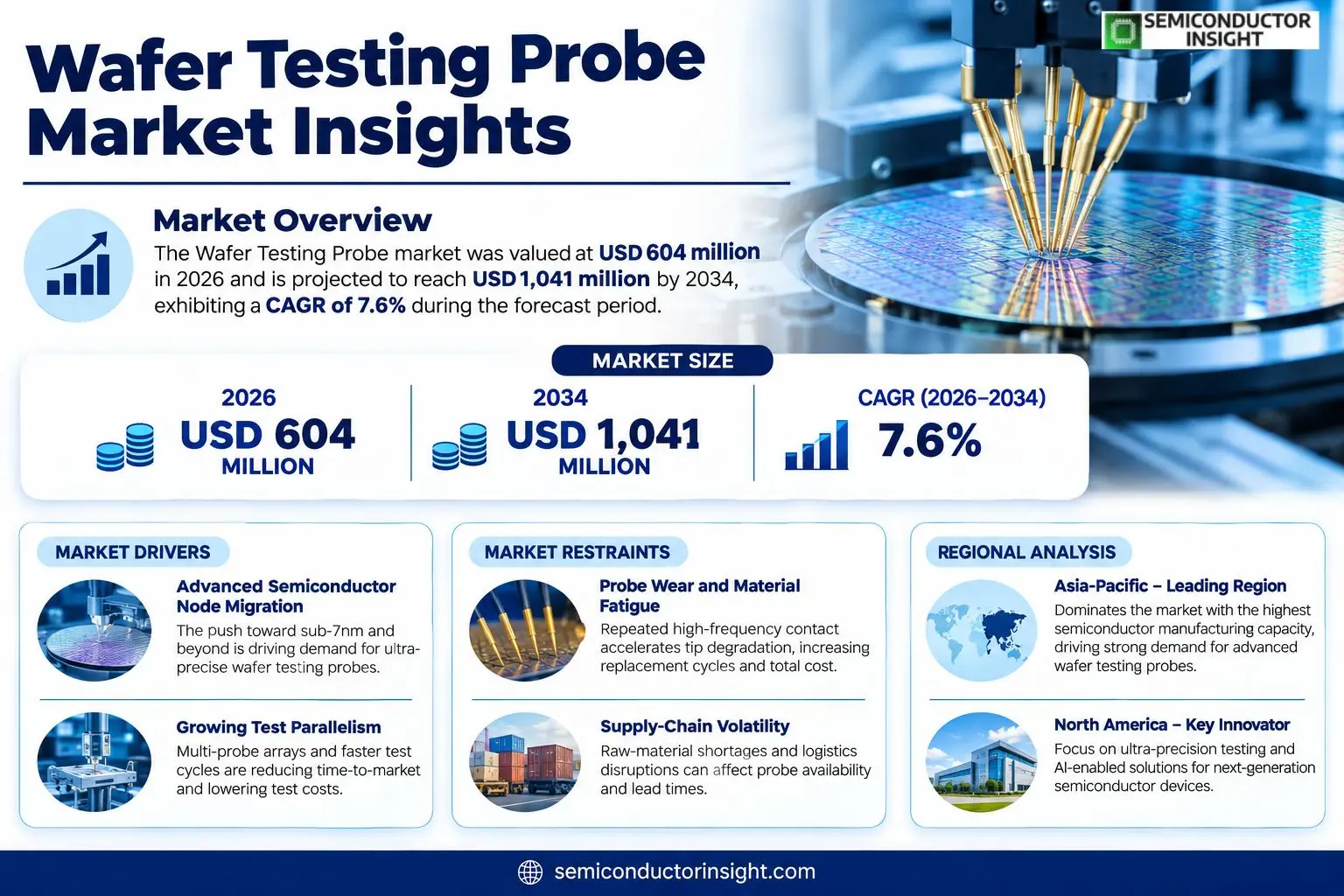
Wafer Testing Probe market was valued at USD 604 million in 2026 and is projected to reach USD 1,041 million by 2034, exhibiting a CAGR of 7.6% during the forecast period.
A Wafer Testing Probe is a critical consumable used in semiconductor wafer electrical testing to establish temporary electrical contact with wafer pads or bumps, typically as part of a probe card. It enables functional, parametric, and reliability testing of dies before dicing, requiring high precision, low contact resistance, and stable signal transmission without damaging the waferespecially for advanced nodes and fine‑pitch applications.The market expands because wafer output grows, advanced‑node migration accelerates, and demand for high‑frequency testing intensifies. In 2026 production reached roughly 710 million units at an average price of USD 932 per unit; capacity stood at about 750 million units. Gross margins range from 20 % to 40 %, while downstream segments such as logic ICs, memory (DRAM/NAND), power semiconductors, analog/RF devices, and advanced packaging sustain demand.
MARKET DRIVERS
Advancements in Semiconductor Lithography
The push toward sub‑10 nm nodes is forcing fabs to adopt ultra‑fine probe arrays that can contact smaller die footprints. Wafer Testing Probe Market players that invest in finer pitch technologies are seeing immediate adoption because manufacturers cannot afford yield loss during test phases.
Cost Pressure for Test‑Time Reduction
Foundries are trimming cycle times to meet aggressive production schedules. Probes engineered for faster make‑break cycles cut overall test duration by roughly 20‑30 %, translating into measurable cost avoidance for high‑volume producers.
➤ Recent field trials show that inline probe kits with integrated micro‑actuators reduce contact‑force variance by 15 %.
These technical gains are reshaping spending patterns: capital allocations are shifting from conventional probe stocks toward modular systems that promise scalability and lower per‑unit test expense.
MARKET CHALLENGES
Probe Wear and Material Fatigue
Repeated high‑frequency contact on delicate wafer surfaces accelerates tip degradation. Even with diamond‑coated solutions, manufacturers report a 10‑12 % increase in replacement cycles once production exceeds 8 k hours, pressuring total cost of ownership.
Other Challenges
Manufacturing Complexity
Fabricating probe pads that align with sub‑micron bump patterns demands multi‑layer lithography and precision etching. The intricate process flow adds lead time, and any yield dip at the probe level propagates downstream to test schedules.
Supply‑Chain Volatility
Raw‑material shortages for high‑purity tungsten and specialty ceramics have led to intermittent stockouts, forcing some fabs to extend the life of aging probe sets beyond optimal performance windows.
MARKET RESTRAINTS
High Capital Expenditure
Acquiring next‑generation probe infrastructure requires multi‑million‑dollar outlays. Smaller contract manufacturers often lack the financial bandwidth to upgrade, resulting in a market segment that remains reliant on legacy equipment and slower test cycles.
MARKET OPPORTUNITIES
Integration with AI‑Enabled Test Platforms
Artificial‑intelligence algorithms are being embedded into test controllers to predict optimal probe pressure and adjust contact timing in real time. Vendors that bundle AI software with probe hardware can offer predictive maintenance packages, opening a service‑revenue stream that enhances client loyalty.
Emerging applications in advanced packagingsuch as fan‑out wafer‑level chip‑scale packagesrequire bespoke probe configurations. Companies that develop rapid‑reconfiguration tooling stand to capture a sizable share of the growing niche, as OEMs look to shorten time‑to‑market for next‑gen devices.
Wafer Testing Probe Market Trends
Advanced Node Migration Fuels Probe Demand
The push of logic devices below the 7 nm threshold has compressed pad dimensions to a degree that only the most precise probing solutions can survive without harming the die. In 2026 the industry churned out roughly 710 million probes at an average price of $932 per unit, a volume that reflects both the sheer scale of wafer output and the necessity for fine‑pitch, low‑resistance contact. End‑users ranging from leading foundries to OSAT specialists rely on these consumables to validate functional, parametric and reliability characteristics before dicing, especially for high‑density memory stacks and chiplet‑based packaging. Wafer Testing Probe Market therefore mirrors the broader semiconductor shift toward heterogeneous integration, as every additional routing layer or stacking step adds a new set of electrical test points that must be accessed reliably. Suppliers that can guarantee uniform tip geometry while sustaining sub‑micron alignment tolerances are positioning themselves as indispensable partners for the next generation of silicon.
Other Trends
Margin Pressure From Material Costs
Specialty alloys and carbide‑based coatings, now commonplace for enhancing durability, have lifted raw‑material outlays by double‑digit percentages over the past year. Companies that own upstream sources or have forged long‑term contracts are preserving gross margins within the historically observed 20‑40 % band; those dependent on spot purchases are seeing margins inch toward the lower threshold. This cost environment is prompting a wave of strategic alliances and selective acquisitions, as midsize manufacturers seek scale to negotiate better terms and to spread R&D expenses across larger production runs. The resulting consolidation subtly reshapes the competitive hierarchy, rewarding players that can balance price stability with the ability to innovate on tip materials and structural designs.
Parallel Testing and High‑Frequency Applications
Test throughput is increasingly defined by parallelism; multi‑probe arrays now enable simultaneous interrogation of dozens of dies, compressing cycle times by as much as thirty percent. Simultaneously, the explosion of 5G infrastructure, automotive radar and high‑speed data‑center processors has heightened the need for probes that transmit high‑frequency signals without adding distortion. Vendors that can demonstrate consistently low contact resistance and uniform signal pathways are locking in multi‑year supply agreements with IDM and packaging firms. These contracts not only smooth revenue streams but also provide a feedback loop for continuous improvement, ensuring that probe designs keep pace with the accelerating cadence of node transitions and the escalating performance expectations of downstream applications.
COMPETITIVE LANDSCAPE
Key Industry Players
Wafer Testing Probe Market Competitive Overview
The wafer testing probe segment is dominated by a handful of multinational firms that leverage deep engineering expertise and sizable production capacity to serve logic, memory and advanced‑packaging customers. Cohu Inc., with its extensive probe‑card portfolio and a global service network, commands the largest share of revenue, largely because its vertical integration permits rapid response to node‑scale shrinkages below 7 nm. LEENO, headquartered in Taiwan, follows closely, differentiating itself through a flexible‑probe technology that reduces contact resistance for fine‑pitch applications. Smiths Interconnect, a legacy player in high‑frequency interconnects, has transitioned its precision‑cantilever line into the probe arena, carving out a niche among RF and analog test engineers. The market structure therefore resembles an oligopoly where a few scale‑rich companies set pricing benchmarks while smaller specialists chase niche segments such as wafer‑level‑packaging or 3D‑stacked memory.Beyond the top tier, a diverse set of regional manufacturers sustains competitive pressure by offering customized geometries, specialty tip materials and rapid prototype cycles. Companies like QA Technology (Japan) and Yokowo Co., Ltd. (Japan) excel in conical‑tip designs that meet emerging chiplet‑testing standards. INGUN (South Korea) and Feinmetall (Germany) focus on high‑durability double‑headed probes suited for high‑throughput foundries. Qualmax (USA) and PTR HARTMANN (Germany) address niche markets such as aerospace‑grade silicon testing, where reliability margins outrank cost considerations. The presence of firms such as Seiken Co., Ltd., TESPRO, AIKOSHA and CCP Contact Probes enriches the ecosystem, providing customers with alternatives that balance price, lead time and technical specificity. This fragmentation encourages continuous innovation, as each player seeks to improve wear resistance, signal integrity and tip‑uniformity to meet the escalating performance demands of next‑generation semiconductor devices.
List of Key Wafer Testing Probe Companies Profiled
- Cohu Inc.
- LEENO
- Smiths Interconnect
- QA Technology
- Yokowo Co., Ltd.
- INGUN
- Feinmetall
- Qualmax
- PTR HARTMANN (Phoenix Mecano)
- Seiken Co., Ltd.
- TESPRO
- AIKOSHA
- CCP Contact Probes
- Da-Chung
- UIGreen
Segment Analysis:
| Segment Category | Sub-Segments | Key Insights |
| By Type |
|
Flexible Probe – Preferred for fine‑pitch nodes due to its inherent compliance and low contact force. – Enables reliable electrical contact on delicate advanced logic and high‑frequency devices. – Supports scaling trends as it tolerates thermal and mechanical stresses during high‑throughput testing. |
| By Application |
|
Packaging and Testing – Drives demand for probes that maintain uniformity across large wafer surfaces. – Critical for advanced packaging like wafer‑level and chiplet solutions where test parallelism is essential. – Requires probes with high durability to withstand repeated contact cycles in high‑volume environments. |
| By End User |
|
Foundries – Emphasize high‑throughput probe solutions to match rapid wafer output growth. – Prioritize probe durability and low contact resistance to reduce downtime. – Seek flexible designs that accommodate a broad portfolio of logic and memory products. |
| By Tip Geometry |
|
Flat‑headed – Favoured for uniform pressure distribution across dense pad arrays. – Enhances signal integrity for high‑frequency testing by minimizing impedance discontinuities. – Aligns well with emerging 3D‑stacked architectures where contact area consistency is paramount. |
| By Structural Configuration |
|
Single‑headed – Simpler architecture that reduces manufacturing complexity and cost. – Provides sufficient performance for mainstream logic and memory testing where extreme parallelism is not required. – Offers ease of integration into existing probe card platforms, accelerating time‑to‑market for testers. |
Regional Analysis: Wafer Testing Probe Market
Foundries in Taiwan and South Korea have upgraded their probe production lines to accommodate higher‑density interconnects. This scaling creates a cascade effect: probe makers must adopt finer tip geometries, and vendors that can re‑tool quickly gain preferential access to the most demanding fabs.
Regional semiconductor clusters channel a sizable portion of their capex into probe‑specific research, exploring materials like graphene for enhanced conductivity. The resulting intellectual property pool raises the entry barrier for newcomers.
Tight logistics networks link probe manufacturers with wafer fabs, reducing buffer inventories. This efficiency enables a just‑in‑time model that aligns probe delivery with wafer launch schedules, minimizing downtime.
Trade agreements across the Asia‑Pacific reduce tariff exposure on high‑tech components, allowing probe suppliers to price competitively while preserving margin on sophisticated probe assemblies.
North America
North America remains a sophisticated market for the Wafer Testing Probe sector, driven largely by the United States’ emphasis on leading‑edge node development. While the region hosts fewer fabs than Asia‑Pacific, the complexity of its production linesparticularly for 5nm and beyondrequires probes with ultra‑high precision and robust data‑capture capabilities. Companies in the United States have increasingly partnered with academic research centres to explore AI‑enhanced defect detection, a trend that could reshape how probe data is interpreted. However, the higher cost structure and regulatory scrutiny around export controls create a friction point for foreign probe makers seeking market entry. Domestic suppliers are therefore focusing on modular probe platforms that can be customised for a range of test scenarios, positioning themselves as flexible providers to both legacy and next‑generation fabs. The strategic implication for vendors is a need to balance price competitiveness with the delivery of highly specialised technical support.
Europe
European wafer manufacturers concentrate on specialty processes such as RF and power devices, which demand probes capable of handling higher voltage tolerances. The region’s strong standards‑driven environment pushes probe makers to certify their products against stringent reliability criteria, fostering a market that values durability over pure performance. Collaboration between leading equipment vendors and research institutes in Germany and the Netherlands has yielded novel probe designs featuring integrated micro‑cooling, addressing the thermal challenges of high‑throughput testing. At the same time, fragmented demand across several mid‑size fabs limits economies of scale, encouraging suppliers to adopt a service‑oriented model that bundles probe lease with on‑site calibration. Providers that can demonstrate compliance with EU environmental directives while offering lifecycle cost efficiencies are likely to secure deeper market penetration.
South America
South America’s semiconductor footprint is modest, yet emerging investments in localized assembly and test facilities hint at a gradual rise in probe requirements. Nations such as Brazil are cultivating micro‑electronics clusters that aim to reduce reliance on imported testing equipment. The market’s nascent stage translates into a preference for cost‑effective, versatile probes that can serve multiple product families. Vendors that supply modular probe kits with straightforward upgrade paths are better positioned to capture early‑adopter contracts. Moreover, the region’s regulatory environment encourages technology transfer agreements, providing an avenue for global probe manufacturers to establish joint‑venture production, thereby mitigating import tariffs and fostering skill development locally.
Middle East & Africa
The Middle East & Africa region exhibits a heterogeneous landscape, with a few high‑tech hubs in the United Arab Emirates and South Africa beginning to explore advanced wafer testing capabilities. Investment incentives aimed at diversifying economies away from hydrocarbons have sparked interest in semiconductor‑related infrastructure, yet the overall market volume remains limited. As a result, probe suppliers focusing on flexible, low‑volume solutionssuch as configurable probe headsfind a niche. Strategic partnerships with local system integrators enable entry into defence and aerospace projects, where reliability and traceability are paramount. The long‑term outlook depends on whether regional policy frameworks continue to nurture a domestic semiconductor ecosystem, which would gradually raise the bar for probe sophistication and create new revenue streams for specialized providers.
Report Scope
This market research report provides a comprehensive analysis of the Wafer Testing Probe Market , covering the forecast period 2026–2034. It offers detailed insights into market dynamics, technological advancements, competitive landscape, and key trends shaping the industry.
Key focus areas of the report include:
- Market Overview: The report begins with an overview outlining its current market scenario, key growth indicators, and industry transformation drivers. It discusses macroeconomic factors, demand–supply balance, regulatory landscape, and the strategic role of semiconductors in powering advancements across industries such as automotive, telecommunications, consumer electronics, and industrial automation.
- Market Size & Forecast: Historical data and future projections for revenue, unit shipments, and market value across major regions and segments.
- Segmentation Analysis: Detailed breakdown by product type, technology, application, and end-user industry to identify high-growth segments and investment opportunities.
- Regional Insights: Insights into market performance across North America, Europe, Asia-Pacific, Latin America, and the Middle East & Africa, including country-level analysis where relevant.
- Competitive Landscape: Profiles of leading market participants, including their product offerings, R&D focus, manufacturing capacity, pricing strategies, and recent developments such as mergers, acquisitions, and partnerships.
- Technology Trends & Innovation: Assessment of emerging technologies, integration of AI/IoT, semiconductor design trends, fabrication techniques, and evolving industry standards.
- Market Drivers & Restraints: Evaluation of factors driving market growth along with challenges, supply chain constraints, regulatory issues, and market-entry barriers.
- Stakeholder Insights: Insights for component suppliers, OEMs, system integrators, investors, and policymakers regarding the evolving ecosystem and strategic opportunities.
Primary and secondary research methods are employed, including interviews with industry experts, data from verified sources, and real-time market intelligence to ensure the accuracy and reliability of the insights presented.
FREQUENTLY ASKED QUESTIONS:
What is the current market size of Wafer Testing Probe Market?
-> Wafer Testing Probe Market was valued at USD 604 million in 2026 and is expected to reach USD 1041 million by 2034, growing at a CAGR of 7.6% during the forecast period.
Which key companies operate in Wafer Testing Probe Market?
-> Key players include LEENO, Cohu, QA Technology, Smiths Interconnect, Yokowo Co., Ltd., INGUN, Feinmetall, Qualmax, PTR HARTMANN (Phoenix Mecano), Seiken Co., Ltd., TESPRO, AIKOSHA, CCP Contact Probes, Da-Chung, UIGreen, Centalic, Woodking Tech, Lanyi Electronic, Merryprobe Electronic, Tough Tech, Hua Rong.
What are the key growth drivers?
-> Key growth drivers include wafer output expansion, migration to advanced nodes below 7 nm, increased test parallelism, rising demand for high‑frequency and high‑speed testing, and growth of advanced packaging and chiplet architectures.
Which region dominates the market?
-> Asia‑Pacific holds the largest share, driven by concentrated semiconductor manufacturing hubs in China, Japan, South Korea, and Taiwan.
What are the emerging trends?
-> Emerging trends include development of fine‑pitch, high‑durability probes, integration of multi‑head probe configurations, and adoption of chiplet‑based testing solutions for advanced packaging.
Get Sample Report PDF for Exclusive Insights
Report Sample Includes
- Table of Contents
- List of Tables & Figures
- Charts, Research Methodology, and more...
 Download Sample Report PDF





