Semiconductor Lithography Equipment Market Insights
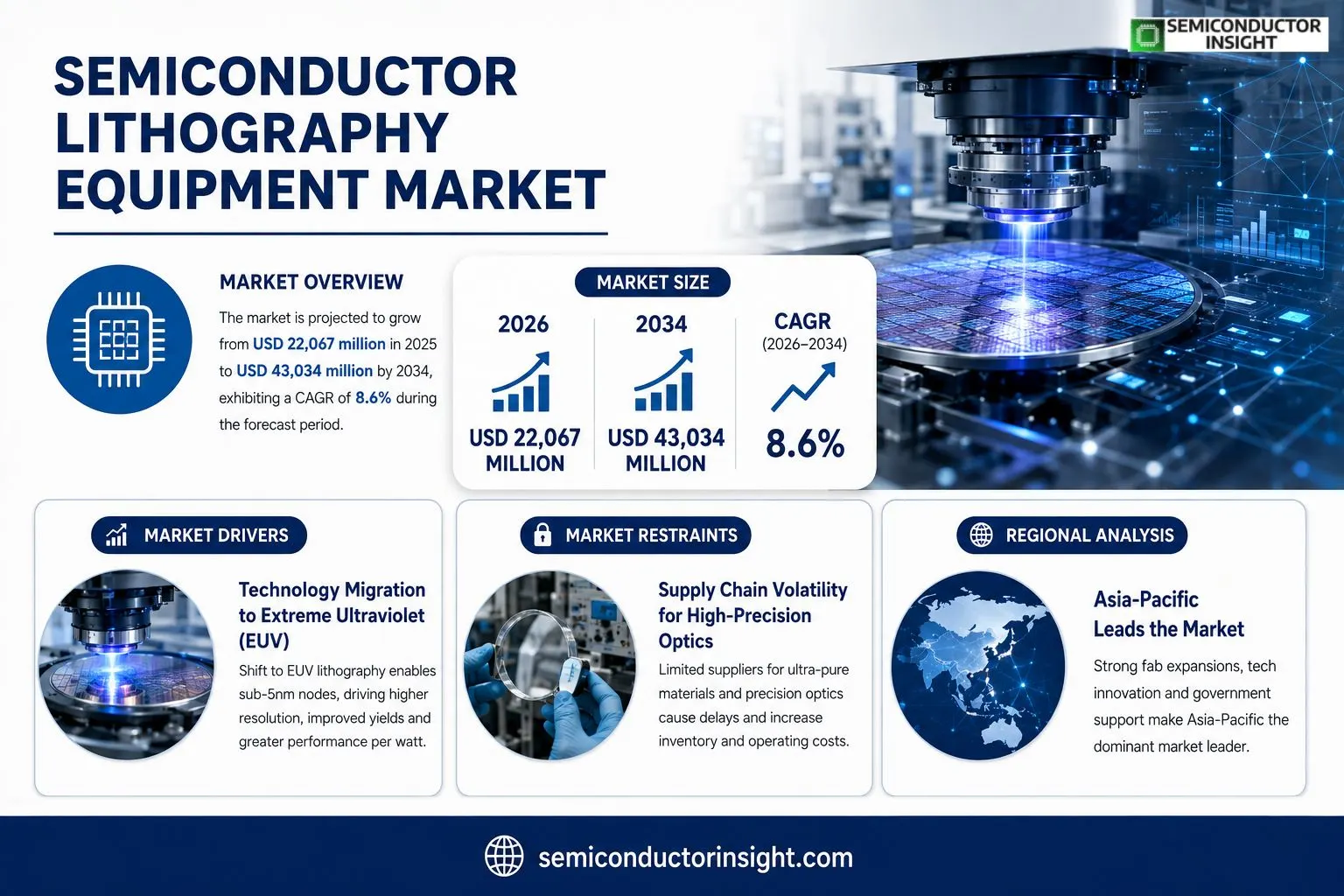
Semiconductor Lithography Equipment market size was valued at USD 22,067 million in 2025 and moves to USD 43,034 million by 2034, reflecting a compound annual growth rate of 8.6% over the forecast horizon.
Semiconductor lithography systems serve as the essential “pattern‑transfer” exposure tools in front‑end wafer fabs and back‑end advanced‑packaging lines. Their primary function is to project or scan circuit patterns from a photomask onto photoresist‑coated wafers (or panels), delivering the resolution, overlay accuracy, and throughput required for subsequent steps such as etch, deposition, and implantation. In practice, mainstream tools are steppers (step‑and‑repeat) and scanners (step‑and‑scan). The technology portfolio spans i‑line (365 nm), KrF (248 nm), ArF (193 nm – both dry and immersion/ArFi) and EUV (13.5 nm), while nanoimprint lithography (NIL) offers a mechanical imprint alternative for selected layers.
MARKET DRIVERS
Technology Migration to Extreme Ultraviolet (EUV)
The transition from deep‑ultraviolet to EUV lithography is reshaping Semiconductor Lithography Equipment Market. Chipmakers pursuing sub‑5 nm nodes demand the higher resolution that EUV provides, prompting manufacturers to accelerate production cycles for next‑generation scanners. This shift is not merely a technical upgrade; it reflects a strategic response to consumer devices that require greater performance per watt.
Capacity Expansion in Asia‑Pacific
Foundries in Taiwan, South Korea and China have announced multi‑billion‑dollar expansions, translating into a surge of equipment orders. The regional emphasis on localized supply chains reduces lead times and aligns procurement with governmental incentives for advanced manufacturing. As a result, equipment makers are witnessing a tangible lift in order backlog.
➤ “The EUV rollout is catalyzing a 7 % annual increase in scanner installations across the top ten fabs,” notes an industry insider.
Beyond technology and geography, the rise of heterogeneous integrationstacking logic, memory and opticscreates a demand for flexible imprint tools capable of handling diverse patterning requirements. Vendors that can offer modular upgrades are positioned to capture premium pricing.
MARKET CHALLENGES
Supply‑Chain Volatility for High‑Precision Optics
Manufacturers rely on a narrow pool of suppliers for ultra‑pure materials and defect‑free mirrors. Recent disruptions in specialty glass production have elongated lead times by up to three months, forcing fabs to adjust fab‑level schedules and allocate additional inventory capital.
Other Challenges
Cost Sensitivity in Mature Nodes
Older process nodes, which still account for a sizable share of output, experience price pressure as customers prioritize cost per wafer over incremental performance gains. This dynamic limits the willingness of budget‑conscious fabs to adopt the latest tool generations.
MARKET RESTRAINTS
Capital Intensity and Return‑on‑Investment Horizons
Each EUV scanner exceeds $150 million, a figure that strains the balance sheets of all but the largest fabs. The lengthy amortization periodoften beyond five yearsdiscourages mid‑size players from committing to the most advanced equipment, thereby capping overall market expansion.
Regulatory Scrutiny on Chemical Usage
Stringent environmental regulations in Europe and North America limit the use of certain photo‑resists and cleaning agents. Compliance requirements add procedural overhead and may delay equipment commissioning, especially for manufacturers that operate across multiple jurisdictions.
MARKET OPPORTUNITIES
Services‑Based Lithography-as-a‑Service (LaaS)
Emerging business models that lease state‑of‑the‑art scanners on a pay‑per‑use basis are gaining traction among fabless designers. LaaS reduces upfront CAPEX, aligns costs with production volume, and offers a pathway for smaller players to access EUV capabilities without bearing the full financial burden.
Integration of AI‑Driven Process Optimization
Embedding machine‑learning algorithms into lithography workflow promises yield improvements of up to 3 %. Vendors that bundle software analytics with hardware differentiate themselves and can command higher margins, opening a lucrative ancillary revenue stream.
Emerging Applications in Quantum and Photonic Chips
The rise of quantum computing prototypes and silicon photonics introduces patterning requirements that differ from classic digital logic. Specialized imprint tools designed for waveguide precision or superconducting circuits represent a nascent yet high‑value segment that early entrants can dominate.
Semiconductor Lithography Equipment Market Trends
High‑NA EUV Adoption Accelerates
The introduction of 0.55 NA High‑NA EUV systems marks a decisive shift in Semiconductor Lithography Equipment Market. By compressing the wavelength to 13.5 nm while increasing numerical aperture, manufacturers can pattern sub‑10 nm layers with fewer multipatterning steps, directly lowering cost‑of‑ownership for leading‑edge logic fabs. Early field installations reported a 15 % rise in throughput per wafer and a measurable reduction in defect density, which translates into higher yields for advanced memory stacks. This technology inflection is not merely a technical upgrade; it reshapes fab capital planning, prompting investors to allocate a larger share of budgets to EUV tooling rather than legacy ArF immersion assets.
Other Trends
Sustained Role of Advanced DUV
Despite the momentum behind EUV, the Advanced DUV segment remains indispensable. ArF immersion platforms continue to dominate the production of semi‑critical layers where resolution demands are modest but overlay precision is paramount. Recent shipments indicate that DUV tools still account for roughly 60 % of total lithography capacity in established fabs. Vendors are pursuing higher numerical apertures within the DUV envelope and integrating AI‑driven process control to squeeze incremental throughput gains. The persistence of DUV safeguards the existing supply chain and provides a buffer for fabs transitioning to full‑scale EUV adoption, especially in regions where capital constraints delay equipment refresh cycles.
Back‑End Lithography Expands with Packaging Needs
The surge in chiplet architectures, 2.5D/3D stacking, and fan‑out panel-level processes is extending lithography’s relevance beyond front‑end wafer formation. High‑overlay, high‑productivity i‑line and specialized NIL systems are finding renewed purpose in redistributing layer (RDL) formation and micro‑bump definition. Analysts note that back‑end exposure tools now represent close to 20 % of the total lithography spend, a share that is projected to climb as data‑center and AI workloads drive more heterogeneous integration. This shift compels equipment makers to broaden their portfolio, offering cost‑effective solutions that balance resolution with cycle time, thereby opening a niche market that is less sensitive to the ultra‑high‑cost dynamics of EUV.
COMPETITIVE LANDSCAPEKey Industry Players
Semiconductor Lithography Equipment Market Competitive Overview
ASML remains the de‑facto gatekeeper of extreme‑ultraviolet (EUV) lithography, commanding roughly nine‑tenths of the EUV shipment pool. Its NXE and EXE families dominate the most advanced logic and memory nodes, and the recent deployment of the first High‑NA EUV system signals a shift from prototype to early‑volume production. This concentration gives ASML substantial pricing leverage, but it also forces customers to synchronize fab roadmaps tightly with the company’s delivery cadence, turning lithography into a strategic bottleneck for leading foundries.Beyond ASML, Nikon and Canon anchor the deep‑ultraviolet (DUV) segment, supplying ArF immersion and KrF scanners that continue to process the bulk of critical layers. Smaller but technically agile firms such as SMEE in China, the Ultratech line now owned by Applied Materials, Dainippon Screen, SUSS MicroTec, Veeco Instruments, Optomec, and KLA‑Tencor’s laser‑direct‑write unit provide niche solutions ranging from i‑line steppers to nano‑imprint tools. These players thrive by targeting cost‑sensitive applications, back‑end packaging, or regional fab expansions where the high‑cost EUV platform is not yet justified.
List of Key Semiconductor Lithography Equipment Companies Profiled
- ASML Holding N.V.
- Nikon Corporation
- Canon Inc.
- Shanghai Micro Electronics Equipment (SMEE)
- Applied Materials – Ultratech Division
- Dainippon Screen Mfg. Co., Ltd.
- SUSS MicroTec AG
- Veeco Instruments Inc.
- Optomec, Inc.
- KLA‑Tencor (laser‑direct‑write business)
- Nanoprecision Ltd.
- Horizon Nanotech (nano‑imprint specialist)
- Micro Link Devices (MLD)
- Sainty Group (i‑line steppers)
- Rohm & Haas Co. (advanced DUV solutions)
Segment Analysis:
| Segment Category | Sub-Segments | Key Insights |
| By Type |
|
EUV Lithography
|
| By Application |
|
Advanced Packaging Lithography
|
| By End User |
|
Logic Device Manufacturers
|
| By Technology Evolution |
|
High‑NA EUV
|
| By Market Drivers |
|
AI/HPC Demand
|
Regional Analysis: Semiconductor Lithography Equipment Market
Asia‑Pacific
Foundries are adding new high‑volume production lines that demand next‑generation lithography tools. The surge in capacity fuels demand for equipment with higher throughput, prompting vendors to accelerate development of faster scanner optics and more robust illumination sources.
Regional alliances between chipmakers and equipment suppliers have birthed joint road‑maps for EUV integration. Collaborative pilots accelerate risk mitigation and embed customer feedback directly into hardware iterations.
The pandemic‑era emphasis on localizing critical inputs has led to diversification of component sources. Vendors are establishing secondary fabs for critical optics and photo‑mask substrates to cushion potential disruptions.
Universities and research institutes in the region supply a steady stream of lithography specialists. This talent pool enables equipment firms to staff advanced engineering teams without geographic lag.
North America
North America remains a pivotal market for high‑end lithography, driven primarily by R&D intensity in the United States. Leading semiconductor designers continue to push the envelope of design complexity, compelling equipment providers to deliver tools that support multi‑patterning and stochastic defect control. The ecosystem benefits from a mature intellectual‑property landscape and a regulatory environment that encourages collaboration between defense agencies and commercial fabs. As a result, vendors focus on differentiating through software analytics and AI‑assisted process optimization, aiming to extract maximal yield from each exposure cycle.
Europe
European players emphasize sustainability and precision engineering within Semiconductor Lithography Equipment Market. The region’s historical strength in optics manufacturing translates into a preference for equipment that balances performance with energy efficiency. Governments across the EU are channeling funding toward “green” chip initiatives, nudging equipment makers to innovate in low‑power laser sources and recyclable component designs. Moreover, stringent data‑privacy regulations shape the architecture of lithography data pipelines, prompting providers to embed secure processing modules directly into the tool stack.
South America
South America’s exposure to the lithography market is modest but evolving as nations aim to reduce import dependency for critical technologies. Emerging fab projects in Brazil and Chile are exploring partnerships with established equipment firms to acquire entry‑level platforms suitable for mature nodes. The market narrative here gravitates around capacity building and workforce development, with local universities initiating lithography‑focused curricula to nurture a pipeline of skilled technicians.
Middle East & Africa
In the Middle East & Africa, strategic interest in semiconductor autonomy is prompting nascent investments in lithography infrastructure. While the region lacks large‑scale fabs, pilot lines are being established in collaboration with equipment vendors to test advanced patterning techniques. The focus is on knowledge transfer and establishing test‑bed environments that can later scale. Policy incentives, such as tax holidays for technology imports, are designed to attract equipment manufacturers willing to explore untapped market potential.
Report Scope
This market research report provides a comprehensive analysis of the Semiconductor Lithography Equipment Market , covering the forecast period 2026–2034. It offers detailed insights into market dynamics, technological advancements, competitive landscape, and key trends shaping the industry.
Key focus areas of the report include:
- Market Overview: The report begins with an overview outlining its current market scenario, key growth indicators, and industry transformation drivers. It discusses macroeconomic factors, demand–supply balance, regulatory landscape, and the strategic role of semiconductors in powering advancements across industries such as automotive, telecommunications, consumer electronics, and industrial automation.
- Market Size & Forecast: Historical data and future projections for revenue, unit shipments, and market value across major regions and segments.
- Segmentation Analysis: Detailed breakdown by product type, technology, application, and end-user industry to identify high-growth segments and investment opportunities.
- Regional Insights: Insights into market performance across North America, Europe, Asia-Pacific, Latin America, and the Middle East & Africa, including country-level analysis where relevant.
- Competitive Landscape: Profiles of leading market participants, including their product offerings, R&D focus, manufacturing capacity, pricing strategies, and recent developments such as mergers, acquisitions, and partnerships.
- Technology Trends & Innovation: Assessment of emerging technologies, integration of AI/IoT, semiconductor design trends, fabrication techniques, and evolving industry standards.
- Market Drivers & Restraints: Evaluation of factors driving market growth along with challenges, supply chain constraints, regulatory issues, and market-entry barriers.
- Stakeholder Insights: Insights for component suppliers, OEMs, system integrators, investors, and policymakers regarding the evolving ecosystem and strategic opportunities.
Primary and secondary research methods are employed, including interviews with industry experts, data from verified sources, and real-time market intelligence to ensure the accuracy and reliability of the insights presented.
FREQUENTLY ASKED QUESTIONS:
What is the current market size of Semiconductor Lithography Equipment Market?
-> Semiconductor Lithography Equipment Market was valued at USD 22,067 million in 2025 and is expected to reach USD 43,034 million by 2034, growing at a CAGR of 8.6% during the forecast period.
Which key companies operate in Semiconductor Lithography Equipment Market?
-> Key players include ASML, Canon, Nikon, SMEE, among others.
What are the key growth drivers?
-> Key growth drivers include AI and high‑performance computing demand, advanced packaging adoption, transition to High‑NA EUV, and increasing lithography intensity per wafer.
Which region dominates the market?
-> Asia-Pacific holds the largest market share, driven by strong semiconductor manufacturing ecosystems in China, Japan, and South Korea.
What are the emerging trends?
-> Emerging trends include High‑NA EUV industrialization, nano‑imprint lithography (NIL) for specific layers, and integration of AI‑enabled lithography optimization tools.
Get Sample Report PDF for Exclusive Insights
Report Sample Includes
- Table of Contents
- List of Tables & Figures
- Charts, Research Methodology, and more...
 Download Sample Report PDF