Photo Mask Inspection Equipment Market Insights
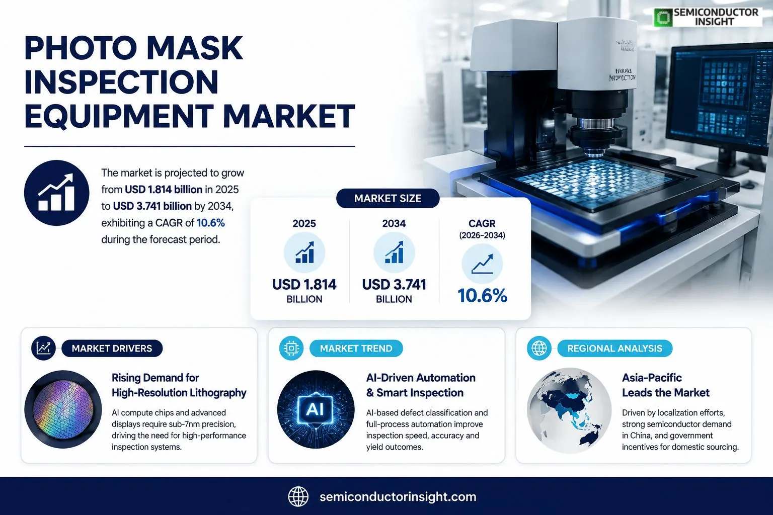
Photo Mask Inspection Equipment market size was valued at USD 1814 million in 2025. The market is projected to grow from USD 1814 million in 2025 to USD 3741 million by 2034, exhibiting a CAGR of 10.6% during the forecast period.
A photomask inspection system examines photomasksthe original masters that transfer integrated‑circuit patterns onto semiconductor wafersfor defects that exceed lithography tolerances. Accurate detection and classification of pattern anomalies are essential for yield protection and cost control because any deviation can propagate through wafer production.The market gains momentum as AI‑compute chips and ultra‑high‑resolution displays push demand for sub‑7 nm mask precision, while high‑NA EUV and curved‑mask technologies create new inspection challenges. Asia‑Pacific, especially China, intensifies domestic sourcing under policy incentives, expanding regional consumption. At the same time, AI‑driven defect discrimination and full‑process automation improve inspection speed and reliability, prompting vendors such as KLA, Applied Materials, Lasertec and Carl Zeiss AG to broaden their portfolios.
MARKET DRIVERS
Increasing Demand for High‑Resolution Semiconductor Lithography
As wafer manufacturers push pattern densities beyond 200 nm, the tolerance for mask defects shrinks dramatically. Precision inspection tools that can identify sub‑micron particles become essential, prompting facilities to upgrade to newer Photo Mask Inspection Equipment Market solutions. The shift reflects a strategic move to safeguard yield and reduce costly re‑work cycles.
Adoption of Advanced Process Nodes
Clients transitioning to 5‑nm and 3‑nm process nodes are forced to adopt inspection platforms capable of handling larger data volumes and higher inspection speeds. Automation and AI‑enhanced defect classification are now viewed as competitive differentiators, because they shorten decision‑making loops and free engineering talent for higher‑value tasks.
➤ “Investors watching Photo Mask Inspection Equipment Market note that each percentage point increase in defect‑free yield translates directly into multi‑million‑dollar profit margins for foundries.”
In parallel, regulatory scrutiny over contamination control in cleanrooms compels manufacturers to document inspection results with greater rigor, reinforcing the business case for next‑generation equipment.
MARKET CHALLENGES
Escalating Capital Requirements
State‑of‑the‑art inspection systems often carry price tags exceeding $2 million, a hurdle for midsize fabs that lack the scale to amortize costs quickly. Budgetary constraints force these players to defer upgrades, creating a bifurcated market where only the largest operators benefit from the latest technology.
Other Challenges
Skill Shortage
Operating sophisticated inspection platforms demands a blend of optical engineering and data analytics expertise. The current talent pool is thin, and training programs have not kept pace with the rapid evolution of analytical software, leading to under‑utilization of available hardware.
MARKET RESTRAINTS
Stringent Validation Protocols
Regulators require extensive validation reports before a new inspection system can be commissioned in a production environment. The time‑intensive documentation process often extends the adoption cycle, delaying revenue realization for equipment suppliers and dampening short‑term market momentum.
MARKET OPPORTUNITIES
Modular Upgrade Paths
Vendors that design inspection platforms with interchangeable optics and plug‑in AI modules enable customers to scale capabilities incrementally. This approach reduces upfront expenditure while preserving a clear upgrade trajectory, opening a revenue stream from existing users seeking incremental enhancements.
Photo Mask Inspection Equipment Market Trends
Demand for Ultra‑High‑Resolution Masks in AI and Advanced Display Segments
The surge in AI‑accelerated computing and the rollout of 4K/8K visual products are forcing semiconductor fabs to tighten mask tolerances beyond the limits of legacy inspection tools. As AI server processors require pattern fidelity at sub‑7nm nodes, any deviation in the photomask quickly translates into yield loss, prompting fab managers to prioritize inspection systems that can resolve sub‑10 nm defects. Likewise, manufacturers of high‑definition panels are shifting to mask designs with denser line/space patterns, which compel equipment suppliers to enhance optical resolution and data‑processing bandwidth. The practical outcome for vendors is a race to embed higher‑resolution sensors and faster scanning optics, while end users gain a clearer pathway to maintain yield as process nodes shrink.
Other Trends
EUV High‑NA and Curved Mask Evolution
High‑numerical‑aperture EUV lithography has moved from prototype to early‑stage production, and the inspection ecosystem is adapting accordingly. Curved masks, introduced to mitigate focus‑related distortions at extreme wavelengths, present a new geometry that traditional flat‑field scanners cannot handle without distortion correction. Equipment manufacturers are therefore redesigning illumination modules and integrating adaptive optics to accommodate the curvature while preserving defect detection sensitivity. Concurrently, high‑NA EUV pushes critical dimension thresholds lower, demanding algorithms capable of distinguishing true defects from stochastic EUV noise. Companies that successfully align hardware upgrades with AI‑driven image analysis are positioned to capture the premium segment of Photo Mask Inspection Equipment Market.
Asia‑Pacific Localization and Supply‑Chain Realignment
Geopolitical considerations and a strategic emphasis on semiconductor self‑reliance have accelerated domestic sourcing of inspection platforms in the Asia‑Pacific, especially China. Policy incentives are encouraging local firms to develop proprietary inspection modules, reducing reliance on imported systems that dominate current installations. While the overall substitution rate for mask blanks remains modest, the upward trajectory of domestically produced inspection units is evident in recent procurement cycles. This shift reshapes competitive dynamics, as multinational vendors must either partner with regional players or localize production to retain market share. For customers, the trend provides greater bargaining power and shorter lead times, ultimately enhancing the agility of Photo Mask Inspection Equipment Market in responding to rapid technology cycles.
COMPETITIVE LANDSCAPEKey Industry Players
Photo Mask Inspection Equipment Market – Competitive Overview
KLA (US) remains the pre‑eminent supplier, commanding roughly one‑third of the 2025 unit shipments. Its AI‑enhanced platforms integrate high‑NA EUV and curved‑mask inspection, giving fab customers the resolution needed for sub‑7 nm nodes. The recent purchase of a defect‑analytics specialist equips KLA with a full‑stack solution that pressures rivals to upgrade software and hardware in lockstep. The overall market shape is oligopolistic, with a small group of corporations holding the bulk of production capacity while boutique firms concentrate on specialty wavelengths or substrate‑only inspection.Applied Materials (US) capitalises on its lithography ecosystem to bundle inspection with upstream tools, whereas Japan’s Lasertec and NuFlare dominate narrow‑band optical designs for 193 nm and EUV masks. Carl Zeiss (Germany) differentiates through metrology‑grade imaging lenses, Advantest (Japan) supplies high‑throughput scanners for volume fabs, and Visionoptech (China) has gained traction as a domestically sourced alternative under supportive policies. New entrants such as ASML’s post‑processing unit, Taiwan’s CVD‑Tech, South Korea’s SPT Co., and Nikon’s inspection division are embedding machine‑learning pipelines, thereby widening the competitive set and raising the technical threshold for newcomers.
List of Key Photo Mask Inspection Equipment Companies Profiled
- KLA Corporation
- Applied Materials
- Lasertec Corp.
- NuFlare Corp.
- Carl Zeiss AG
- Advantest Corp.
- Visionoptech Co., Ltd.
- ASML Post‑Processing
- CVD‑Tech Ltd.
- SPT Co.
- Nikon Corporation
- Hitachi High‑Tech Corp.
- MKS Instruments, Inc.
Segment Analysis:
| Segment Category | Sub-Segments | Key Insights |
| By Type |
|
Photomask Inspection Equipment
|
| By Application |
|
Semiconductor IC/Chip Manufacturer
|
| By End User |
|
Photomask Factory
|
Regional Analysis: Photo Mask Inspection Equipment Market
North America
The bulk of high‑volume production sits in California’s Silicon Valley and Texas, where large fabs integrate inspection stations directly into their photolithography lines, fostering tight feedback loops that accelerate process optimization.
Federal export controls on advanced lithographic tools shape supplier strategies, encouraging local sourcing of critical components and prompting firms to diversify their supply base within the continent.
Early adopters leverage AI‑enhanced defect detection, which shortens inspection cycles and enables real‑time corrective actions, setting a performance baseline that competitors quickly emulate.
Proximity to semiconductor material providers curtails lead times for critical optics, while regional logistics hubs ensure rapid deployment of service teams for on‑site calibration and maintenance.
Europe
European manufacturers capitalize on a strong tradition of precision optics, translating to photo mask inspection systems renowned for reliability. Countries such as Germany and the Netherlands host clusters where equipment makers collaborate closely with research institutes, fostering incremental innovation around metrology standards. Clients in the region prioritize robustness and compliance with stringent environmental directives, which pushes suppliers to embed energy‑efficient designs. Although the market size trails North America, the emphasis on quality and regulatory alignment positions Europe as a crucible for resilient, long‑life equipment offerings.
Asia-Pacific
The Asia‑Pacific corridor, anchored by Taiwan, South Korea, and emerging players in China, reflects a rapid scaling of semiconductor capacity. Demand for inspection solutions is fueled by aggressive node roadmaps, compelling vendors to push resolution limits while maintaining affordable pricing structures. Local fabs often partner with equipment providers for joint development, resulting in customized platforms that address specific process windows. Nevertheless, the region grapples with uneven talent distribution, prompting firms to invest heavily in training programs that blend optical engineering with data analytics.
South America
South American activity remains nascent, centered around a handful of mature fabs in Brazil and a growing interest from regional research facilities. Market participants view inspection equipment as a strategic acquisition to attract multinational investors seeking end‑to‑end manufacturing capabilities. Cost sensitivity dominates purchasing decisions, steering buyers toward modular systems that can be expanded as capacity grows. While the overall market depth is limited, the region’s openness to technology transfer creates opportunities for OEMs willing to offer flexible financing and localized support.
Middle East & Africa
In the Middle East and Africa, the market is characterized by exploratory investments linked to national semiconductor initiatives and smart‑manufacturing pilots. Governments are establishing technology parks that demand state‑of‑the‑art inspection tools to signal credibility to partners. Procurement here is often driven by long‑term strategic goals rather than immediate production needs, encouraging suppliers to provide turnkey solutions that include training, remote diagnostics, and integration services. The nascent demand, combined with a desire for knowledge transfer, positions the region as a future growth frontier for Photo Mask Inspection Equipment Market.
Report Scope
This market research report provides a comprehensive analysis of the Photo Mask Inspection Equipment Market , covering the forecast period 2026–2034. It offers detailed insights into market dynamics, technological advancements, competitive landscape, and key trends shaping the industry.
Key focus areas of the report include:
- Market Overview: The report begins with an overview outlining its current market scenario, key growth indicators, and industry transformation drivers. It discusses macroeconomic factors, demand–supply balance, regulatory landscape, and the strategic role of semiconductors in powering advancements across industries such as automotive, telecommunications, consumer electronics, and industrial automation.
- Market Size & Forecast: Historical data and future projections for revenue, unit shipments, and market value across major regions and segments.
- Segmentation Analysis: Detailed breakdown by product type, technology, application, and end-user industry to identify high-growth segments and investment opportunities.
- Regional Insights: Insights into market performance across North America, Europe, Asia-Pacific, Latin America, and the Middle East & Africa, including country-level analysis where relevant.
- Competitive Landscape: Profiles of leading market participants, including their product offerings, R&D focus, manufacturing capacity, pricing strategies, and recent developments such as mergers, acquisitions, and partnerships.
- Technology Trends & Innovation: Assessment of emerging technologies, integration of AI/IoT, semiconductor design trends, fabrication techniques, and evolving industry standards.
- Market Drivers & Restraints: Evaluation of factors driving market growth along with challenges, supply chain constraints, regulatory issues, and market-entry barriers.
- Stakeholder Insights: Insights for component suppliers, OEMs, system integrators, investors, and policymakers regarding the evolving ecosystem and strategic opportunities.
Primary and secondary research methods are employed, including interviews with industry experts, data from verified sources, and real-time market intelligence to ensure the accuracy and reliability of the insights presented.
FREQUENTLY ASKED QUESTIONS:
What is the current market size of Photo Mask Inspection Equipment Market?
-> Photo Mask Inspection Equipment Market was valued at USD 1814 million in 2025 and is expected to reach USD 3741 million by 2034, at a CAGR of 10.6% during the forecast period.
Which key companies operate in Photo Mask Inspection Equipment Market?
-> Key players include KLA (US), Applied Materials (US), Lasertec (JP), NuFlare (JP), Carl Zeiss AG (DE), Advantest (JP), Visionoptech (CN).
What are the key growth drivers?
-> Key growth drivers include high‑resolution mask demand driven by AI compute chips and 4K/8K displays, technological iteration toward EUV and curved masks, and AI‑enabled automation for defect detection.
Which region dominates the market?
-> Asia‑Pacific holds the largest share and is the fastest‑growing region, driven by localization efforts and strong demand in China.
What are the emerging trends?
-> Emerging trends include integration of AI for defect discrimination, automation of full‑process inspection, high‑NA EUV mask inspection, and adoption of curved mask technology.

Get Sample Report PDF for Exclusive Insights
Report Sample Includes
- Table of Contents
- List of Tables & Figures
- Charts, Research Methodology, and more...
 Download Sample Report PDF