PBN Crucibles for Semiconductor Market Insights
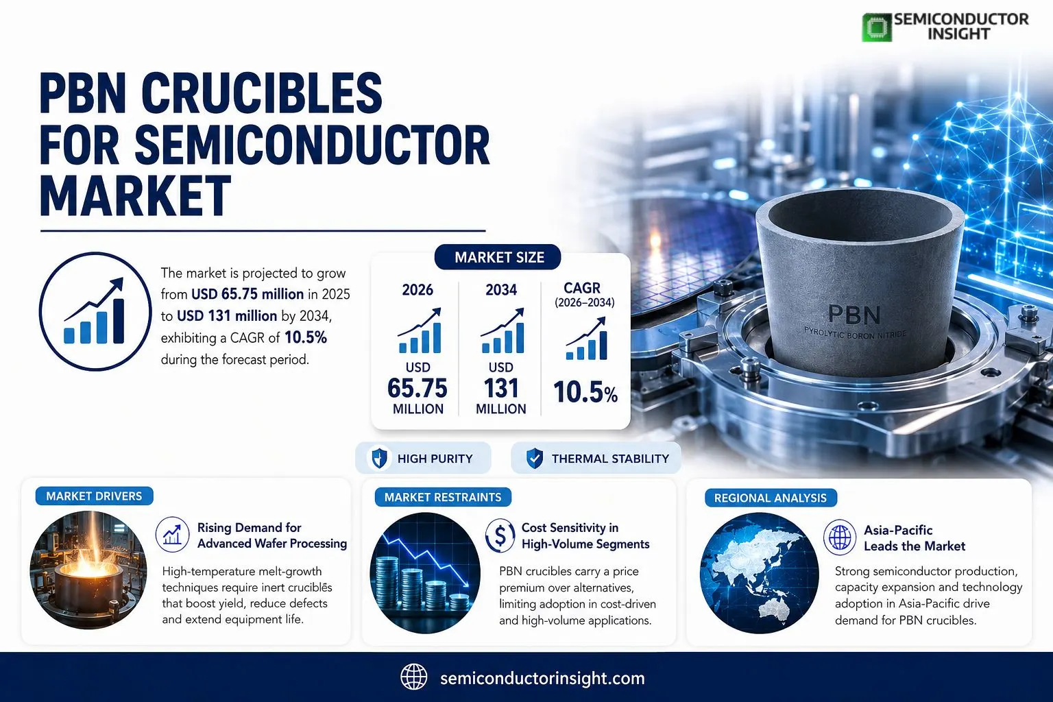
PBN Crucibles for Semiconductor market was valued at USD 65.75 million in 2025 and is projected to reach USD 131 million by 2034, exhibiting a CAGR of 10.5% during the forecast period.
Semiconductor PBN crucibles are high‑temperature functional ceramic components fabricated primarily from high‑purity pyrolytic boron nitride deposited by chemical vapor deposition onto graphite substrates. They serve as containers for molten feedstock or evaporation sources in compound‑semiconductor single‑crystal growth (e.g., GaAs, InP) and ultra‑high‑vacuum epitaxy processes such as MBE, LEC and VGF. Their non‑porous structure delivers extremely low outgassing, strong thermal‑shock resistance and stable chemical inertness, which prevents impurity release and composition drift under stringent cleanliness requirements.The market gains momentum because expanding compound‑semiconductor production, advanced packaging initiatives and OLED display manufacturing increase demand for contamination‑free, thermally uniform crucible solutions. Government policies aimed at strengthening domestic semiconductor supply chains further encourage investment in high‑purity materials, reinforcing the outlook for PBN crucible suppliers.
MARKET DRIVERS
Rising Demand for Advanced Wafer Processing
The semiconductor foundry segment is expanding its use of high‑temperature melt‑growth techniques, which places a premium on crucible materials that can withstand repeated thermal cycling without contaminating the melt. PBN Crucibles for Semiconductor Market meet these criteria, offering superior chemical inertness that directly translates into higher wafer yield and lower defect density.
Stricter Purity Standards
Customers are tightening specifications for trace metal levels in crystal growth environments. The ultra‑low impurity profile of polycrystalline boron nitride (PBN) makes it a preferred choice for manufacturers seeking to maintain sub‑ppb contamination thresholds. This shift not only validates the premium pricing of PBN crucibles but also creates a defensible market niche.
➤ Manufacturers that integrate PBN crucibles into their production lines can reduce re‑work costs by up to 15 % while extending equipment life cycles.
In parallel, the rollout of next‑generation node technologies (sub‑5 nm) intensifies the need for materials that resist outgassing and lattice perturbations. By delivering a stable thermal environment, PBN Crucibles for Semiconductor Market enable tighter process windows, which is essential for meeting the performance targets of emerging devices.
MARKET CHALLENGES
Capital Intensity of Equipment Upgrades
Adopting PBN crucibles often requires retrofitting existing melt‑growth furnaces to accommodate the crucible geometry and thermal expansion characteristics. The upfront investment, combined with the need for specialized handling protocols, can deter smaller fabs from making the switch.
Other Challenges
Supply Chain Visibility
The raw materials for producing high‑purity PBN are sourced from a limited number of suppliers, which can lead to lead‑time volatility. Clients must develop robust forecasting models to avoid production bottlenecks.Furthermore, the niche nature of the product means that many semiconductor manufacturers lack in‑house expertise on PBN handling, necessitating additional training resources and potentially slowing adoption rates.
MARKET RESTRAINTS
Cost Sensitivity in High‑Volume Segments
Although PBN crucibles deliver clear performance benefits, their price premium remains a barrier for high‑volume, cost‑driven production lines such as those serving legacy logic devices. Price‑elastic segments tend to prioritize lower‑cost alumina or quartz alternatives, limiting broader market penetration.
MARKET OPPORTUNITIES
Expansion into 3‑D Integrated Circuit Manufacturing
3‑D IC processes increasingly rely on wafer bonding and through‑silicon‑via (TSV) formation, both of which benefit from the high thermal stability of PBN crucibles. Suppliers that position their products as critical enablers for 3‑D integration can capture a growing share of the next‑generation device market.Additionally, emerging applications in quantum computing and sensor technologies demand ultra‑pure crystal substrates. PBN Crucibles for Semiconductor Market are uniquely positioned to meet the stringent contamination controls required for these high‑value niches, presenting a lucrative avenue for targeted growth.
PBN Crucibles for Semiconductor Market Trends
Material Purity as a Competitive Lever
PBN Crucibles for Semiconductor Market hinges on the ability of manufacturers to deliver containers that do not introduce trace contaminants into III‑V crystal growth or OLED evaporation processes. High‑purity pyrolytic boron nitride, deposited by chemical vapor deposition, delivers a non‑porous, low‑outgassing surface that stabilises thermal fields and prevents composition drift in sensitive materials such as GaAs, InP and emerging GaP devices. Customers therefore treat each crucible as a yield‑preserving component rather than a disposable item, reinforcing the premium pricing of tightly‑toleranced, custom‑size products. The data set shows a valuation of $65.75 million in 2025 and a rise to $131 million by 2034, confirming that end‑users are allocating more budget to contamination‑critical tooling as wafer sizes increase and device architectures demand tighter process windows.
Other Trends
Technology Barriers and Manufacturing Complexity
Achieving uniform CVD deposition across large graphite substrates remains a bottleneck; minor thickness variations translate into thermal gradients that compromise crystal uniformity. Moreover, machining of intricate liners demands specialised equipment capable of preserving the inert surface without inducing micro‑cracks. Companies that have invested in closed‑loop deposition monitoring and precision CNC tooling are able to offer longer‑life crucibles with fewer out‑gassing incidents, which in turn drives higher customer retention. The barrier to entry is therefore a blend of materials science expertise and advanced manufacturing capability, limiting the field to a handful of firms that can satisfy the rigorous qualification cycles of semiconductor fabs.
Geographic Shifts and Policy Influence
Regional policy frameworks in the United States, Europe and China are channeling investment toward domestic supply‑chain resilience, indirectly boosting demand for locally sourced PBN crucibles. While the policies do not earmark crucibles specifically, the surge in funding for compound‑semiconductor fabs, advanced packaging lines and OLED display plants creates upstream pressure for high‑purity containers. Japanese and U.S. firms retain early‑mover advantages through established CVD lines and long‑term customer qualifications, yet Chinese manufacturers are expanding capacity and broadening product portfolios to address domestic fab requirements. This evolving landscape suggests that future growth will be shaped by a dual strategy: premiumisation of ultra‑pure, complex‑shaped crucibles for high‑margin applications, and localisation of production to meet regional content mandates.
COMPETITIVE LANDSCAPE
Key Industry Players
PBN Crucibles: Technological Edge and Regional Concentration
The market continues to be anchored by a handful of legacy manufacturers that combine deep CVD expertise with long‑standing qualification programs in leading semiconductor fabs. Shin‑Etsu Chemical Co., Ltd. dominates the high‑purity segment, leveraging its early adoption of pyrolytic BN deposition to secure supply contracts for GaAs and InP single‑crystal growers in Japan and the United States. Momentive Technologies follows closely, differentiating through a broad portfolio of PBN‑coated graphite liners that address the thermal‑shock demands of molecular‑beam epitaxy equipment. Both firms maintain a pricing premium justified by ultra‑low outgassing metrics, which translates into higher yield for downstream wafer production. Morgan Advanced Materials and Luxel Corporation round out the Western core, offering specialized tooling that integrates seamlessly with VGF and LEC reactors while preserving the tight impurity budgets required by advanced packaging lines.Beyond the established core, a growing cohort of Chinese and Korean players is reshaping the competitive calculus. Companies such as Vital Materials Co., Limited, Shandong Glojin New Material Co., Ltd., and Beijing Boyu Semiconductor Vessel Craftwork Technology Co., Ltd. have expanded capacity through government‑backed subsidies, allowing them to deliver customized crucible geometries at a fraction of legacy pricing. Xiamen Powerway Advanced Material Co., Ltd. and Xiamen Mascera Technology Co., Ltd. focus on niche OLED evaporation cells, where rapid turnaround and design flexibility are decisive. Korean entrant Hwasin Material Co., Ltd. couples precision CNC machining with in‑house CVD, targeting the high‑volume MBE segment. While these newcomers lack the decades‑long qualification record of the Japanese and U.S. incumbents, their aggressive investment in thin‑film uniformity and supply‑chain localisation is narrowing the performance gap and forcing the market toward a more fragmented, yet technologically vibrant, landscape.
List of Key PBN Crucibles for Semiconductor Companies Profiled
- Shin-Etsu Chemical Co., Ltd.
- Momentive Technologies
- Luxel Corporation
- Morgan Advanced Materials
- Thermic Edge Ltd
- Veeco Instruments Inc.
- Scienta Omicron
- Vital Materials Co., Limited
- Shandong Glojin New Material Co., Ltd.
- Beijing Boyu Semiconductor Vessel Craftwork Technology Co., Ltd.
- Xiamen Powerway Advanced Material Co., Ltd.
- Hwasin Material Co., Ltd.
Segment Analysis:
| Segment Category | Sub-Segments | Key Insights |
| By Type |
|
PBN LEC Crucibles
|
| By Application |
|
GaAs Single Crystal Growth
|
| By End User |
|
Compound Semiconductor Manufacturers
|
| By Material Structure |
|
Solid PBN
|
| By Delivery Form |
|
Standalone Crucible
|
Regional Analysis: PBN Crucibles for Semiconductor Market
Asia‑Pacific
Fab expansions in Shanghai and Singapore have triggered a surge in PBN crucible orders, as larger reactors demand vessels that can sustain uniform temperature gradients. Suppliers are scaling melt‑shop output to match this uptick, while also offering modular designs that can be retrofitted into existing lines.
The shift toward 300 mm and emerging 450 mm wafer formats forces fabs to evaluate crucible materials that minimize impurity diffusion. PBN’s low vapor pressure and high melting point make it a preferred choice, prompting R&D collaborations that test new alloy coatings inside the crucible interior.
Recent geopolitical tensions have highlighted the need for diversified sources of high‑purity PBN. Vendors are establishing secondary manufacturing sites in Vietnam and Malaysia to hedge against export restrictions and to shorten delivery cycles for critical fab upgrades.
Environmental standards in Japan and South Korea now require tighter control of hazardous emissions during crucible production. This has spurred investments in cleaner sintering processes, which not only comply with regulation but also improve the micro‑structural consistency of the final PBN product.
North America
U.S. and Canadian fabs continue to rely on legacy quartz containers, yet a handful of high‑volume manufacturers are piloting PBN crucibles to address yield concerns on advanced node projects. The principal barrier remains the perceived cost premium, which is being mitigated through performance‑based leasing models that allow fabs to defer upfront expense while capturing efficiency gains.
Europe
European semiconductor players, especially in Germany and the Netherlands, are integrating PBN crucibles within niche equipment for power‑device production. The region’s strong emphasis on sustainability drives adoption, as PBN’s longer service life translates into reduced material waste and lower overall carbon footprints for the manufacturing process.
South America
Brazil’s emerging semiconductor cluster is still in the early adoption phase, with local equipment integrators evaluating PBN crucibles for specialty applications such as silicon‑carbide devices. Partnerships with Asian suppliers are forming to import expertise, and the market’s growth will likely hinge on government incentives that lower the entry cost for PBN technology.
Middle East & Africa
The Middle East’s investment in high‑tech manufacturing zones has attracted a modest number of fab projects that view PBN crucibles as a differentiator for product reliability. In Africa, pilot programs in South Africa’s research institutes are exploring PBN’s resistance to harsh processing environments, laying groundwork for future industrial uptake.
Report Scope
This market research report provides a comprehensive analysis of the PBN Crucibles for Semiconductor Market , covering the forecast period 2026–2034. It offers detailed insights into market dynamics, technological advancements, competitive landscape, and key trends shaping the industry.
Key focus areas of the report include:
- Market Overview: The report begins with an overview outlining its current market scenario, key growth indicators, and industry transformation drivers. It discusses macroeconomic factors, demand–supply balance, regulatory landscape, and the strategic role of semiconductors in powering advancements across industries such as automotive, telecommunications, consumer electronics, and industrial automation.
- Market Size & Forecast: Historical data and future projections for revenue, unit shipments, and market value across major regions and segments.
- Segmentation Analysis: Detailed breakdown by product type, technology, application, and end-user industry to identify high-growth segments and investment opportunities.
- Regional Insights: Insights into market performance across North America, Europe, Asia-Pacific, Latin America, and the Middle East & Africa, including country-level analysis where relevant.
- Competitive Landscape: Profiles of leading market participants, including their product offerings, R&D focus, manufacturing capacity, pricing strategies, and recent developments such as mergers, acquisitions, and partnerships.
- Technology Trends & Innovation: Assessment of emerging technologies, integration of AI/IoT, semiconductor design trends, fabrication techniques, and evolving industry standards.
- Market Drivers & Restraints: Evaluation of factors driving market growth along with challenges, supply chain constraints, regulatory issues, and market-entry barriers.
- Stakeholder Insights: Insights for component suppliers, OEMs, system integrators, investors, and policymakers regarding the evolving ecosystem and strategic opportunities.
Primary and secondary research methods are employed, including interviews with industry experts, data from verified sources, and real-time market intelligence to ensure the accuracy and reliability of the insights presented.
FREQUENTLY ASKED QUESTIONS:
What is the current market size of PBN Crucibles for Semiconductor Market?
-> PBN Crucibles for Semiconductor Market was valued at USD 65.75 million in 2025 and is expected to reach USD 131 million by 2034, growing at a CAGR of 10.5% during the forecast period.
Which key companies operate in PBN Crucibles for Semiconductor Market?
-> Key players include Shin-Etsu Chemical Co., Ltd.; Momentive Technologies; Luxel Corporation; Morgan Advanced Materials; Thermic Edge Ltd; Veeco Instruments Inc.; Scienta Omicron; Vital Materials Co., Limited; Shandong Glojin New Material Co., Ltd.; Beijing Boyu Semiconductor Vessel Craftwork Technology Co., Ltd.; Xiamen Powerway Advanced Material Co., Ltd.; Xiamen Mascera Technology Co., Ltd.; Summit-Tech Resource Corp.; Hwasin Material Co., Ltd.
What are the key growth drivers?
-> Key growth drivers include rising demand for high‑purity, low‑outgassing, high‑temperature‑resistant components in compound‑semiconductor crystal growth (GaAs, InP), ultra‑high‑vacuum epitaxy (MBE), and OLED evaporation; supportive semiconductor policies in China, the United States and Europe that reinforce domestic supply‑chain resilience; and the market’s move toward premiumization and localization of PBN crucible supply.
Which region dominates the market?
-> Asia‑Pacific holds the largest market share, driven by strong production capabilities in China, Japan and South Korea, while North America (U.S.) and Europe remain important secondary markets.
What are the emerging trends?
-> Emerging trends include premiumization of PBN crucibles with higher purity, more complex structures and longer service life; regional localization of material supply ecosystems; and expanded application scope into advanced packaging, display evaporation and next‑generation compound semiconductor manufacturing.
Get Sample Report PDF for Exclusive Insights
Report Sample Includes
- Table of Contents
- List of Tables & Figures
- Charts, Research Methodology, and more...
 Download Sample Report PDF