Flip-Chip Package Substrate Market Insights
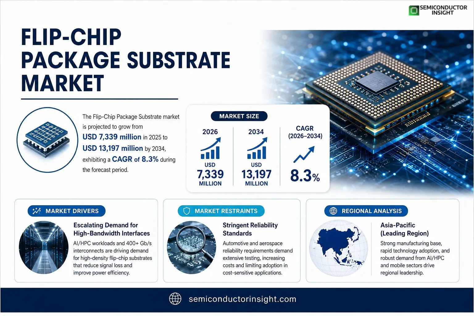
Flip-Chip Package Substrate market size was valued at USD 7,339 million in 2025. The market is projected to grow from USD 7,339 million in 2025 to USD 13,197 million by 2034, exhibiting a CAGR of 8.3% during the forecast period.
A Flip-Chip Package Substrate (flip-chip package substrate / IC substrate for flip-chip) is the high-density interconnect structure between a flip-chipped die and the system PCB, providing I/O fan-out, power/ground distribution, high-speed routing, mechanical support, and a controlled path for thermal conduction. In industry practice the most common product families are FC-BGA substrates (for CPUs/GPUs/AI accelerators, networking ASICs and other large high-I/O packages) and FC-CSP substrates (for mobile processors, RF front-end modules and compact SiP platforms). The dominant construction is the organic build-up substrate; Ajinomoto explicitly positions ABF as an essential material for forming the multi-layer “CPU bed” that connects nanometer-scale die terminals to millimeter-scale board-level terminals via laser processing and direct copper plating.The market is experiencing growth because AI/HPC workloads are pushing demand for larger package sizes and higher I/O density while heterogeneous integration drives tighter signal‑integrity budgets and greater power/thermal requirements. SEMI reports indicate that supply constraints have already emerged for advanced substrates prompting manufacturers such as Samsung Electro-Mechanics and AT&S to invest in glass-core technologies and fine-line SAP processes. Recent announcements include Samsung’s development of glass-core substrates for high-end server CPUs and AT&S’s rollout of high-reliability microvia stacks to support massive pin-count escape routing.
MARKET DRIVERS
Escalating Demand for High‑Band‑width Interfaces
Flip‑Chip Package Substrate Market is being propelled by the surge in data‑center bandwidth requirements. As servers adopt 400 Gb/s and higher interconnects, manufacturers turn to flip‑chip substrates because they reduce signal loss and support finer pitch configurations. This shift enables OEMs to meet latency targets while maintaining power efficiency, a combination that directly influences procurement decisions.
Growth of Advanced Mobile and Automotive Electronics
Mobile processors now integrate heterogeneous functions on a single die, and automotive ADAS modules demand rugged, high‑temperature substrates. Flip‑chip packages deliver the mechanical robustness and thermal performance required for these applications, encouraging tier‑1 suppliers to allocate larger budgets toward substrate redesigns. The resulting volume lift is evident in the recent uptick of multi‑chip module shipments.
➤ Design teams are shortening time‑to‑market by 15 % through the adoption of flip‑chip substrates that consolidate routing layers.
Beyond performance, the cost advantage of consolidating ball‑grid‑array (BGA) footprints into a single flip‑chip layout is reshaping pricing negotiations. Buyers are increasingly evaluating total cost of ownership rather than nominal component cost, a perspective that favors the efficiencies inherent in this substrate technology.
MARKET CHALLENGES
Complexity of Materials Qualification
Achieving reliable performance across temperature extremes requires rigorous validation of organic versus ceramic substrates. The learning curve associated with new laminate formulations inflates engineering overhead, especially for midsize firms lacking dedicated R&D resources. Consequently, some players hesitate to commit capital until pilot runs demonstrate consistent yield.
Other Challenges
Supply‑Chain Fragmentation
The reliance on a limited pool of high‑purity copper foils and low‑dielectric‑constant polymers creates bottlenecks. Recent geopolitical tensions have exposed vulnerabilities, prompting customers to reevaluate inventory strategies and negotiate longer lead‑times, which can dampen short‑term growth momentum.
MARKET RESTRAINTS
Stringent Reliability Standards
The automotive and aerospace segments impose failure‑rate thresholds that are difficult to meet without extensive testing cycles. Meeting these standards often necessitates additional under‑fill materials and enhanced inspection protocols, driving up production costs and limiting the appeal of flip‑chip substrates for cost‑sensitive applications.
Limited Design‑Tool Ecosystem
While mainstream PCB design suites have incorporated basic support for flip‑chip layouts, advanced electromagnetic simulation tools remain scarce. The absence of seamless integration forces engineers to rely on third‑party plugins, extending design timelines and increasing the risk of inadvertent design errors.
MARKET OPPORTUNITIES
Emergence of 3D‑IC Integration
The convergence of 3D‑IC stacking and flip‑chip substrates opens a lucrative avenue for Flip‑Chip Package Substrate Market. By enabling vertical interconnects, manufacturers can unlock higher functional density without expanding board real‑estate. Early adopters are already securing design wins in AI accelerators, suggesting a runway of multi‑year growth for substrate providers that can align their processes with 3D‑IC roadmaps.
Flip-Chip Package Substrate Market Trends
AI‑Driven Scaling of Flip‑Chip Substrate Complexity
The surge in AI accelerators and high‑performance computing chips forces substrate manufacturers to push I/O pin counts beyond traditional limits. Designers now request fine‑line SAP, microvia stacks that survive laser drilling, and copper plating sequences that keep resistance low while preserving signal integrity. This technical pressure translates into larger panel formats and multilayer organic build‑up films, where ABF acts as the connective “CPU bed” linking nanometer‑scale die pads to millimeter‑scale board terminals. For OEMs, the ability to deliver a substrate that tolerates higher power density while maintaining flatness directly influences time‑to‑market for next‑generation servers. Consequently, suppliers that can synchronize dielectric chemistry with laser‑drill reliability gain leverage in price negotiations and secure longer supply contracts.
Other Trends
Material Innovations and Warpage Control
Glass‑core substrates have emerged as a practical answer to the warpage challenges that accompany wider panel sizes. By replacing conventional organic cores with a glass layer, manufacturers attain superior thermo‑mechanical stability, reducing the risk of delamination during reflow. Parallel to this, ABF formulations are being tweaked to enhance thermal conductivity, allowing die temperatures to stay within safe margins even as power envelopes climb. These material advances not only improve yield but also open avenues for embedding passive components within the substrate, thereby shrinking overall package footprint. Companies that invest in joint R&D with equipment vendors report a measurable lift in first‑pass success rates, which in turn lowers inventory holding costs for system integrators.
Consolidation of Substrate Supply Chain
The ecosystem surrounding Flip‑Chip Package Substrate Market is tightening around a core group of dielectric producers, high‑volume substrate factories, and a handful of OSAT partners. Recent mergers among mid‑size substrate makers have created entities with the scale needed to run 12‑inch panel lines, while strategic alliances with equipment manufacturers ensure access to the latest laser‑drill and plating tools. This concentration reduces the likelihood of material shortages that previously plagued high‑I/O projects, yet it raises entry barriers for new players. For customers, the shift means more predictable lead times but also fewer sources to negotiate on price, prompting many to diversify their design portfolios across multiple substrate types to mitigate supply risk.
COMPETITIVE LANDSCAPE
Key Industry Players
Flip‑Chip Package Substrate Market – Competitive Overview
Among the manufacturers, Unimicron commands the largest share of high‑density FC‑BGA output, leveraging a vertically integrated supply chain that blends proprietary ABF film development with advanced laser‑drill microvia technology. This integration allows the firm to sustain high volume yields while meeting the stringent thermal‑stability requirements of next‑generation CPUs and AI accelerators. The company’s strategic placement of fabs in Taiwan and China gives it a logistical advantage that reinforces its leadership in both the server‑grade and consumer‑grade segments.Beyond the dominant tier, a second wave of specialized playerssuch as Ibiden, Nan Ya PCB, Shinko Electric Industries, Kinsus Interconnect Technology, AT&S, Samsung Electro‑Mechanics, Kyocera, Toppan, Zhen Ding Technology, Daeduck Electronics, LG InnoTek, Shennan Circuit, Shenzhen Fastprint Circuit Tech, Korea Circuit, AaltoSemi, and ASE Materialfocus on niche product families like FC‑CSP, glass‑core substrates, or embedded passive solutions. Their competitive edge stems from differentiated material stacks, aggressive adoption of fine‑line SAP processes, or close collaborations with OSATs that tailor substrate designs to heterogeneous integration roadmaps. Collectively, these firms intensify pressure on pricing and accelerate innovation cycles across the ecosystem.
List of Key Flip‑Chip Package Substrate Companies Profiled
- Unimicron
- Unimicron
- Ibiden
- Nan Ya PCB
- Shinko Electric Industries
- Kinsus Interconnect Technology
- AT&S
- Samsung Electro‑Mechanics
- Kyocera
- Kyocera
- Toppan
- Zhen Ding Technology
- Daeduck Electronics
- LG InnoTek
- Shennan Circuit
- Shenzhen Fastprint Circuit Tech
- Korea Circuit
- AaltoSemi
- ASE Material
Segment Analysis:
| Segment Category | Sub-Segments | Key Insights |
| By Type |
|
FC‑BGA Substrate is the dominant type because it supports the highest I/O density and thermal performance for demanding server‑grade CPUs and AI accelerators.
|
| By Application |
|
AI/HPC Chips drive the most intensive substrate requirements due to extreme power‑density and signal‑integrity challenges.
|
| By End User |
|
OSATs are the primary end users because they execute high‑volume flip‑chip assembly and require substrates that align with flexible panel‑scale processes.
|
| By Material |
|
ABF Substrate is favored for high‑performance flip‑chip packages because it delivers exceptional dielectric stability and enables fine‑line patterning.
|
| By Technology Trend |
|
Glass‑Core Substrates are emerging as a strategic technology for large‑form‑factor packages due to their exceptional flatness and thermo‑mechanical stability.
|
Regional Analysis: Flip-Chip Package Substrate Market
Cities such as Shanghai, Singapore, and Seoul host concentrated R&D clusters where substrate engineers experiment with nano‑scale laminates, generating IP that quickly migrates to production lines across the region.
Multi‑tiered logistics networks reduce dependency on single sources, allowing manufacturers to source copper foils and dielectric films from several neighboring economies without major disruptions.
A surge in contract design houses offers end‑customers turnkey solutions that integrate substrate layout with chip‑level routing, shortening development cycles for complex system‑in‑package offerings.
Competitive labor costs and government incentives keep overall fabrication expenses lower than in Western markets, encouraging global OEMs to source substrates from the region.
North America
North America remains a strong demand generator, especially for high‑end computing platforms that require ultra‑reliable interconnects. Leading fab operators collaborate with substrate specialists to push the limits of thermal management, a priority for data‑center deployments. While the region lacks the same manufacturing scale as Asia‑Pacific, its emphasis on precision engineering and intellectual property creates a premium market segment that values performance over cost.
Europe
European manufacturers focus on sustainability, integrating recyclable materials and low‑temperature processing into substrate production. Regulatory frameworks push for greener supply chains, prompting firms to differentiate through eco‑friendly credentials. At the same time, automotive electrification drives demand for robust substrates that can endure harsh thermal cycles, positioning Europe as a niche hub for reliable, compliant solutions.
South America
South America’s market is shaped by modest domestic consumption and a growing interest in localized assembly to avoid import tariffs. Countries such as Brazil are nurturing partnerships between university research labs and substrate vendors, aiming to build a modest but self‑sufficient ecosystem that can serve regional telecommunications upgrades.
Middle East & Africa
The Middle East & Africa region is gradually building capability through joint ventures with Asian manufacturers. Investment in smart‑city infrastructure and edge‑computing nodes generates a nascent demand for compact, high‑density substrates. Although overall volumes remain limited, the strategic focus on diversification of tech imports is prompting early‑stage development projects.
Report Scope
This market research report provides a comprehensive analysis of the Flip-Chip Package Substrate Market , covering the forecast period 2026–2034. It offers detailed insights into market dynamics, technological advancements, competitive landscape, and key trends shaping the industry.
Key focus areas of the report include:
- Market Overview: The report begins with an overview outlining its current market scenario, key growth indicators, and industry transformation drivers. It discusses macroeconomic factors, demand–supply balance, regulatory landscape, and the strategic role of semiconductors in powering advancements across industries such as automotive, telecommunications, consumer electronics, and industrial automation.
- Market Size & Forecast: Historical data and future projections for revenue, unit shipments, and market value across major regions and segments.
- Segmentation Analysis: Detailed breakdown by product type, technology, application, and end-user industry to identify high-growth segments and investment opportunities.
- Regional Insights: Insights into market performance across North America, Europe, Asia-Pacific, Latin America, and the Middle East & Africa, including country-level analysis where relevant.
- Competitive Landscape: Profiles of leading market participants, including their product offerings, R&D focus, manufacturing capacity, pricing strategies, and recent developments such as mergers, acquisitions, and partnerships.
- Technology Trends & Innovation: Assessment of emerging technologies, integration of AI/IoT, semiconductor design trends, fabrication techniques, and evolving industry standards.
- Market Drivers & Restraints: Evaluation of factors driving market growth along with challenges, supply chain constraints, regulatory issues, and market-entry barriers.
- Stakeholder Insights: Insights for component suppliers, OEMs, system integrators, investors, and policymakers regarding the evolving ecosystem and strategic opportunities.
Primary and secondary research methods are employed, including interviews with industry experts, data from verified sources, and real-time market intelligence to ensure the accuracy and reliability of the insights presented.
FREQUENTLY ASKED QUESTIONS:
What is the current market size of Flip-Chip Package Substrate Market?
-> Flip-Chip Package Substrate Market was valued at USD 7339 million in 2025 and is expected to reach USD 13197 million by 2034 with a CAGR of 8.3% during the forecast period.
Which key companies operate in Flip-Chip Package Substrate Market?
-> Key players include Unimicron, Ibiden, Nan Ya PCB, Shinko Electric Industries, Kinsus Interconnect Technology, AT&S, Samsung Electro-Mechanics, Kyocera, Toppan, Zhen Ding Technology, Daeduck Electronics, Zhuhai Access Semiconductor, LG InnoTek, Shennan Circuit, Shenzhen Fastprint Circuit Tech, Korea Circuit, FICT LIMITED, AKM Meadville, Shenzhen Hemei Jingyi Semiconductor Technology, Simmtech, HOREXS, ASE Material, AaltoSemi.
What are the key growth drivers?
-> Key growth drivers include AI and HPC demand, heterogeneous integration, rising I/O density, higher power and thermal requirements for servers and accelerators, and expanding adoption of advanced packaging technologies.
Which region dominates the market?
-> Asia is the dominant region, driven by strong production capacity in China, Japan, and South Korea, while also showing the fastest growth.
What are the emerging trends?
-> Emerging trends include UHDI scaling with fine-line SAP, glass‑core substrate development, embedded passives/actives, advanced microvia stacks, and multifunctional core designs for improved thermal and mechanical stability.
Get Sample Report PDF for Exclusive Insights
Report Sample Includes
- Table of Contents
- List of Tables & Figures
- Charts, Research Methodology, and more...
 Download Sample Report PDF