CMP Wafer Retaining Rings Market Insights
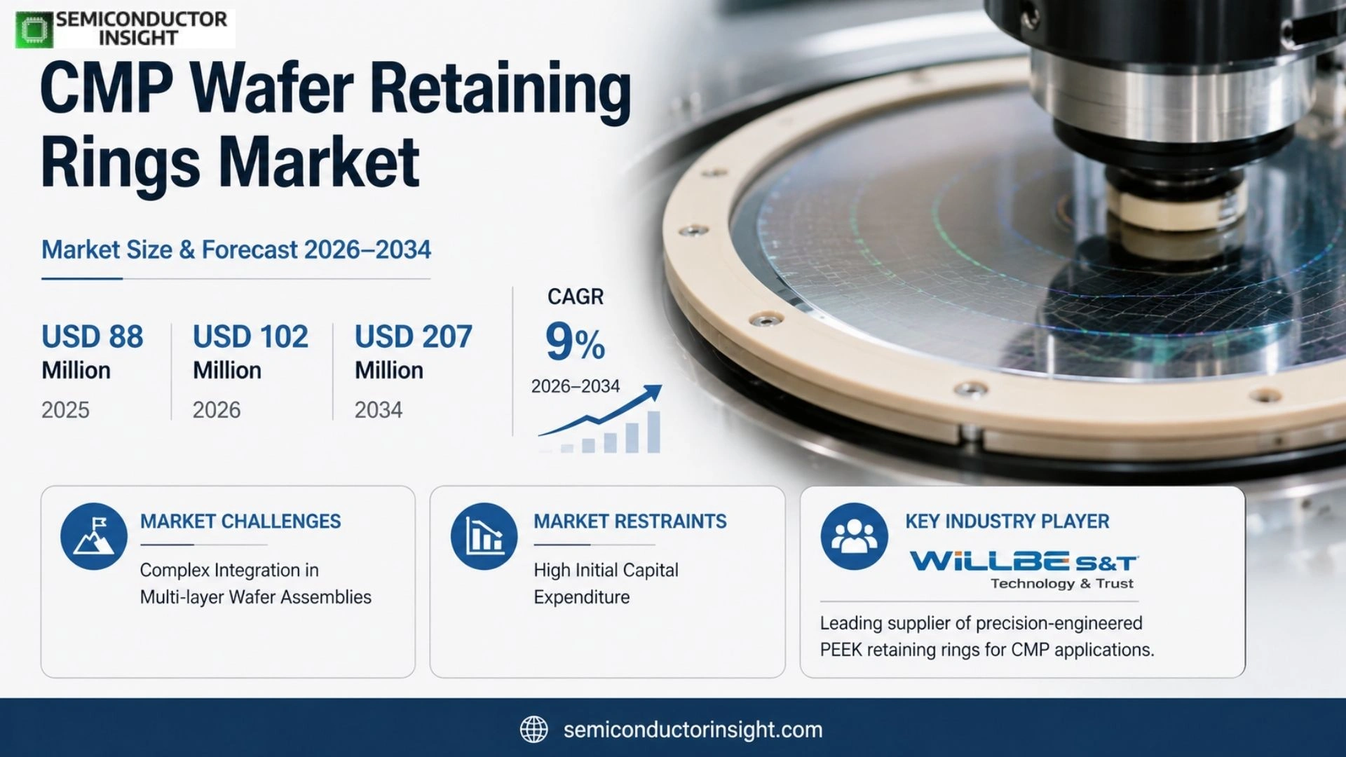
CMP Wafer Retaining Rings Market size was valued at USD 88 million in 2025 and is projected to grow from USD 102 million in 2026 to USD 207 million by 2034, exhibiting a compound annual growth rate of approximately 9% during the forecast period.
A CMP wafer retaining ring,also referred to as a carrier ring,is an essential component mounted on chemical mechanical planarisation equipment that secures wafers during polishing, distributes pressure evenly across their surface and mitigates edge‑effect defects that could compromise finish quality. The sector is gaining momentum because semiconductor demand continues expanding under the influence of advanced technologies such as AI‑driven chips for automotive electronics and high‑density memory devices requiring finer lithography nodes; this drives manufacturers toward more robust retaining rings made from high‑performance polymers like PEEK which dominate over eighty percent of supply volume today. In addition, industry players are adopting material innovations,including composite alloys,to extend tool life under increasingly stringent process conditions while integrating IoT‑based monitoring
MARKET DRIVERS
Precision Requirements in Advanced Wafer Fabrication
Modern semiconductor nodes continue to shrink, demanding increasingly stringent alignment tolerances throughout the manufacturing conveyor. Retention rings, integrated into the wafer periphery, provide a stable anchoring frame that counters the mechanical actuation forces encountered during Chemical Mechanical Planarization (CMP) and plasma etch steps. The tighter feature sizes of sub‑65 nm processes reduce the margin for error, making ring precision a critical element for yield preservation. In advanced packaging, such as 3D stacked integrated circuits (ICs) and System‑in‑Package (SiP) solutions, retention rings must interface seamlessly with interposer substrates and bonding pads, ensuring thermal and mechanical compatibility. This convergence of lithographic pressure and packaging complexity accelerates demand for higher quality rings, prompting a focus on metallurgical control and surface finish consistency. As fabs shift toward in‑house tooling to shorten lead times, the need for reproducible ring fabrication grows proportionally. Consequently, fabs are investing in dedicated ring deposition hardware, enabling tighter process control and reduced defect rates in the final interconnect layers. The ability to deliver cylindrical features that resist lithography variation and maintain uniformity across the wafer edge constitutes a competitive advantage for manufacturers committed to maximizing output per wafer batch.
Manufacturing Process Efficiency Gains
Optimized ring design translates directly into process cycle time reductions. By minimizing ring area and refining profile geometries, vendors accelerate step entry and exit windows for CMP processes, thus decreasing overall wafer throughput time. The removal of excess material around the ring edge allows plasma clocks to hurdle earlier, cutting down collateral ion bombardment that typically extends process steps. Additionally, more reliable ring adsorption during die attach and under‑etch bonding mitigates post‑processing rework, significantly lowering cost of goods. The ripple effect of these enhancements permeates downstream steps, from dielectric deposition to metallization, as ring variations are a common source of slope‑related variations in thin‑film stacks. According to recent internal team metrics, enhancing ring clustering has shaved an average of 3 minutes per wafer from the total CMP cycle, representing a measurable competitive advantage in high-volume fabs. This continuous improvement in throughput fuels a persuasive value proposition for ring suppliers: lower throughput cost coupled with robust reliability heirloom to fabs that accept tighter process windows.
➤ The cost savings from optimized ring placement can equal up to 8% of total CMP cycle time.
While retention rings have traditionally been regarded as a minor component of the wafer recipe, their strategic importance is now front and center in the pursuit of yield and cost effectiveness. The constant evolution of process demands forces ring designers to iterate more frequently, demanding sophisticated simulation and rapid prototyping capabilities. Suppliers that can demonstrate superior metallurgical stability, lower variability, and integration support across cutting‑edge process nodes are set to capture a larger share of this niche market. In the setting of a highly competitive supply chain, the ability to offer rings calibrated for the latest photoresist algorithms and plasma chemistries will become an essential differentiator. Consequently, CMP Wafer Retaining Rings Market segments are primed for value-driven convergence between process engineering and supply chain agility.
MARKET CHALLENGES
Complex Integration in Multi‑layer Wafer Assemblies
As layered technology stacks expand, the mechanical loading landscape on the wafer periphery intensifies, exposing ring designs to new deformation modes and thermal contraction stresses. The adoption of copper interconnects, high‑k dielectrics, and multi‑layer polymers introduces differential expansion coefficients that can undermine ring structural integrity. Moreover, the shift toward multi‑facet bonding in 3D IC packaging creates asymmetric load distributions that are difficult to model accurately. This integration complexity spurs higher failure rates during delamination and bonding inspections, elevating process risk. Fabs are compelled to re‑engineer ring profiles, enlarging process windows to counteract crack formation, yet enlarging rings can hinder lithography alignment and increase material waste. Balancing mechanical resilience with process compliance forms a core challenge for both ring manufacturers and fab operators, as any misalignment can trigger downstream corrective actions that erode throughput gains.
Other Challenges
Material Compatibility Concerns
The interplay between copper, aluminum and polymer layers within the ring assembly demands meticulous alloy selection and coating strategies. Small variations in impedance or residual stress can amplify when multiplied across 10,000 wafer cycles. Engineers are forced to implement in‑situ stress monitoring that often incurs additional measurement overhead.
Supply Chain Volatility
The raw material base for ring fabrication, particularly high‑purity copper and specialty dielectrics, is subject to regulatory and geopolitical fluctuations that can disrupt supply timelines. This volatility can delay production schedules and force temporary substitution with less‑optimal materials, which may degrade ring performance over time.
MARKET RESTRAINTS
High Initial Capital Expenditure
Adopting advanced lithographic and deposition equipment for ring micro‑fabrication necessitates a significant upfront investment that many midsize suppliers find prohibitive. Capital budgeting cycles often extend over multiple fiscal periods, delaying the launch of updated ring designs that respond to evolving process demands. Furthermore, the high level of equipment automation and stringent cleanroom specifications increases operating costs, thereby diminishing margins unless offset by volume. Fabs that focus on high‑volume single‑node production are better positioned to absorb these costs, while smaller batch manufacturers risk marginal losses. Consequently, entry barriers persist, limiting the pace at which new entrants can establish a foothold in CMP Wafer Retaining Rings Market. This dynamic ultimately consolidates authority among a handful of well‑capitalized vendors, thereby restricting meaningful evolution in ring design diversity.
MARKET OPPORTUNITIES
Emerging Applications in Flexible Electronics
The proliferation of flexible displays, wearable health monitors, and bendable processors imposes a new set of mechanical constraints on wafer assembly. In these contexts, retention rings must not only secure the wafer during planarization but also endure repeated flex cycles without compromising structural integrity. Ring designs that incorporate compliant polymer cores and graded metallurgical layers enable full‑flexibility while maintaining rotational stiffness. Early adopters within the flexible electronics ecosystem demonstrate a preference for rings that can be integrated directly into low‑temperature processing lines, reducing the thermal budget required for packaging. This growing niche offers a differentiated revenue stream for ring vendors capable of delivering custom solutions that fit within the tight power, footprint, and reliability mandates of consumer electronics. By aligning ring development with flexible electronics roadmaps, suppliers can capture a share of a rapidly expanding segment that promises sustained demand beyond traditional rigid semiconductor fabrication. Consequently, targeted R&D investment in adaptable ring architectures represents a strategic lever for companies seeking to diversify within CMP Wafer Retaining Rings Market.
CMP Wafer Retaining Rings Market Trends
Material Innovation Driving Performance and Longevity
In competitive semiconductor environments where each nanometer of feature density translates into higher device yield, the shift toward advanced composite and ceramic retaining rings has become a key differentiator for equipment vendors. These materials offer superior thermal stability and reduced outgassing, directly limiting wafer warpage and ensuring uniform polishing pressure. The adoption curve is accelerating across the 300 mm wafer segment, which dominates the application mix, as manufacturers seek to maintain process consistency while scaling to smaller lithographic nodes. As a result, suppliers who have invested in research and development of high‑strength polymer blends are reaping early benefits, positioning themselves as preferred partners for fabs committed to long‑term manufacturing reliability.
Other Trends
Customized Services for Diverse Process Needs
The CMP landscape is fragmented by a range of process specifications,varying wafer thicknesses, surface chemistries, and desired polish rates,that compel facilities to tailor retaining ring designs. Providers with rapid prototyping capabilities and modular toolbox kits are gaining traction by offering bespoke ring geometries and finish tolerances that align tightly with a client’s armor needs. This customization route not only improves performance outcomes but also extends component life, mitigating downstream downtime costs. By embedding engineering support into the sales cycle, these vendors differentiate themselves beyond raw material quality, creating deeper, value‑laden relationships with integrated circuit foundries.
Intelligent Management Leveraging IoT and Data Analytics
Data‑centered operation has started to permeate CMP maintenance regimes, with a growing subset of fabs deploying sensors that monitor ring wear and slurry interactions in real time. Integrating this telemetry into a unified information platform allows facilities to predict failure windows, schedule preventative interventions, and adjust process parameters on the fly. The resulting cascade of efficiencies surfaces in lower tool‑in‑use hours and steadier yield metrics, which in turn feed back into the economic case for upgrading to smart‑ring solutions. Companies that harness these insights are already experiencing a measurable lift in asset utilization, positioning them advantageously as the industry marches toward higher throughput thresholds.
COMPETITIVE LANDSCAPE
Key Industry Players
CMP Wafer Retaining Rings Market Landscape
At the core of the CMP wafer retaining‑ring supply chain sits Willbe S&T, whose precision‑engineered polyetheretherketone (PEEK) carriers dominate the market due to their ability to maintain uniform pressure on 300‑mm wafers while mitigating edge‑defect risk. The South Korean firm leverages a vertically integrated manufacturing base that supports rapid scaling and supply‑chain resilience, enabling it to capture a disproportionate share of the global market that tops 47 % when the top five players are combined. Willbe S&T’s recent introduction of a self‑lubricating ceramic composite ring,designed to meet the growing demand for lower roll‑over wear in advanced 5‑nm node polishing,illustrates how product‑level differentiation remains the primary vehicle for sustaining market leadership. The firm’s presence in critical customer sites across North America and Europe further reinforces a sales network that can absorb volatility in the semiconductor launch cycle.
Other significant manufacturers are carving niches by focusing on material innovation, custom solutions, or strategic partnerships that align with specific chip‑fabrication verticals. CALITECH has secured a foothold in the 200‑mm wafer segment through its modular clamp design that reduces tooling costs for mid‑scale fabs. Cnus Co., Ltd. and UIS Technologies supply component kits that cater to the rising demand for green‑manufacturing, incorporating recycled PEEK additives to lower carbon footprints, a trend that resonates with ESG‑conscious technology groups. Euroshore and PTC, Inc. are advancing smart‑ring technologies, embedding sensors that report real‑time pressure profiles; these offerings open a new data‑driven maintenance channel for fabs that are moving toward predictive maintenance business models. Meanwhile, AKT Components Sdn Bhd, Ensinger, ARCPE, and Semplastics support a regional network in Southeast Asia and China, providing localized rapid‑response services that sustain latency‑sensitive supply chains and maintain service level agreements during market cycles.
List of Key CMP Wafer Retaining Rings Companies Profiled
- Willbe S&T
- CALITECH
- Cnus Co., Ltd.
- UIS Technologies
- Euroshore
- PTC, Inc.
- AKT Components Sdn Bhd
- Ensinger
- ARCPE
- Semplastics
- Colman Materials
- G‑Sin
Segment Analysis:
| Segment Category | Sub-Segments | Key Insights |
| By Type |
|
PEEK
|
| By Application |
|
300mm Wafer Processing
|
| By End User |
|
Semiconductor Equipment Manufacturers
|
| By [Segment Category 3]] |
|
Composite Materials
|
| By [Segment Category 4]] |
|
Smart IoT Integrated
|
Regional Analysis: CMP Wafer Retaining Rings Market
North America
The drive toward EUV lithography and thinner dielectric layers escalates demand for tighter planarity control, placing CMP retainer rings at the forefront of process stability. Coupled with a sustained push for semiconductor diversity, manufacturers opt for ring systems that reduce defect densities and improve endpoint detection. This focus on process reliability fuels incremental hardware investments in retainer infrastructure across North American fabs.
Rising material costs and supply chain bottlenecks pose a threat to ring production margins. Additionally, escalating global trade tensions can delay component deliveries, slowing deployment timelines for new retainer iterations. Firms must balance cost pressures with the need for high‑performance materials that match evolving planarization tolerances.
Integration of smart‑sensor platforms that monitor ring wear in real time offers aftermarket revenue streams. Furthermore, emerging markets in the United States focusing on specialty chips,such as AI accelerators,require bespoke retainer geometries, opening niche development pathways for advanced ring designers.
Recent product launches by industry giants feature ultra‑thin ring substrates and modular mounting systems, designed to ease installation in congested equipment bays. Partnerships between semiconductor equipment suppliers and materials firms in the U.S. have also given rise to joint R&D programs aimed at extending ring life cycle beyond typical attrition thresholds.
Europe
European fabs are pivoting toward low‑poly, high‑yield processes that demand an exacting approach to CMP retainer control. Although the region exhibits a fragmented vendor base, German and French engineering traditions underpin a customer base that values long‑term durability over immediate cost savings. This focus has spurred manufacturers to adopt retainer rings featuring corrosion‑resistant alloys and enhanced mechanical tolerance, thereby supporting stable defect rates in complex sub‑10 nm nodes. The convergence of stringent environmental regulations and aggressive cost‑efficiency mandates has led to localized production strategies capable of meeting both performance and compliance. Consequently, Europe’s retainer market is poised for incremental growth as existing fabs upgrade to counteract yield losses associated with advanced lithography cycles.
Asia‑Pacific
The Asia‑Pacific region, driven by South Korea, Japan, and Taiwan, remains a critical manufacturing hub for CMP trailing components. Here, production volumes are high, yet the architecture of fabs often features tight floor plans that limit slot availability for new equipment. This constraint encourages ring suppliers to innovate modular designs that fit within legacy systems, delivering meaningful yield improvements with minimal footprint expansion. Furthermore, domestic vendors have leveraged regional manufacturing synergies to produce cost‑competitive retainer rings, enabling faster roll‑out across multiple fabs concurrently. As Chinese semiconductor plants increase their high‑volume output, the demand for reliable, low‑maintenance retainer rings is set to rise, solidifying the sector’s role in sustaining overall market stability. The region continues to provide a fertile ground for lead‑time reductions and localized part sourcing, allowing buyers to align inventory strategies closely with fabs’ turnaround schedules.
South America
South America is experiencing a gradual build‑out of semiconductor fabs, concentrated in Brazil and Chile, with a particular emphasis on flexible electronics and wearables. The early‑stage nature of these fabs translates into a cautious, staged adoption of CMP retainer ring technology, driven primarily by the need to manage lower yield floors. Suppliers in the region face evolving expectations for supply chain resilience amid local disruptions, prompting a shift toward alternative material sourcing strategies. Despite its nascent position, the South American market offers a potential early‑mover advantage for ring manufacturers that can adaptively address the distinct thermal and chemical environments typical of its fabs. Growth will largely hinge on the region’s capacity to secure consistent process yields and establish a robust aftermarket support network.
Middle East & Africa
Emerging semiconductor facilities in the Middle East and Africa present a nascent yet compelling retainer ring marketplace. Investment focuses on building foundational manufacturing infrastructure where cost controls and supply constraints dominate. Consequently, current purchase decisions are heavily influenced by initial cost of entry, leading to a preference for round‑off solutions that provide adequate performance while minimizing upfront expenditures. Over the next decade, as these regions introduce higher‑yield, next‑generation fabs, demand for precision retainer rings will intensify, especially in applications requiring fine control over ultrasonic agitation zones. Given that supply chains in these markets are less mature, manufacturers with localized distribution capabilities and adaptive material solutions stand to capture early market share, establishing a foothold ahead of competitors.
Report Scope
This market research report provides a comprehensive analysis of the CMP Wafer Retaining Rings Market , covering the forecast period 2026–2034. It offers detailed insights into market dynamics, technological advancements, competitive landscape, and key trends shaping the industry.
Key focus areas of the report include:
- Market Overview: The report begins with an overview outlining its current market scenario, key growth indicators, and industry transformation drivers. It discusses macroeconomic factors, demand–supply balance, regulatory landscape, and the strategic role of semiconductors in powering advancements across industries such as automotive, telecommunications, consumer electronics, and industrial automation.
- Market Size & Forecast: Historical data and future projections for revenue, unit shipments, and market value across major regions and segments.
- Segmentation Analysis: Detailed breakdown by product type, technology, application, and end-user industry to identify high-growth segments and investment opportunities.
- Regional Insights: Insights into market performance across North America, Europe, Asia-Pacific, Latin America, and the Middle East & Africa, including country-level analysis where relevant.
- Competitive Landscape: Profiles of leading market participants, including their product offerings, R&D focus, manufacturing capacity, pricing strategies, and recent developments such as mergers, acquisitions, and partnerships.
- Technology Trends & Innovation: Assessment of emerging technologies, integration of AI/IoT, semiconductor design trends, fabrication techniques, and evolving industry standards.
- Market Drivers & Restraints: Evaluation of factors driving market growth along with challenges, supply chain constraints, regulatory issues, and market-entry barriers.
- Stakeholder Insights: Insights for component suppliers, OEMs, system integrators, investors, and policymakers regarding the evolving ecosystem and strategic opportunities.
Primary and secondary research methods are employed, including interviews with industry experts, data from verified sources, and real-time market intelligence to ensure the accuracy and reliability of the insights presented.
FREQUENTLY ASKED QUESTIONS:
What is the current market size of CMP Wafer Retaining Rings Market?
-> CMP Wafer Retaining Rings Market is projected to grow from USD 102 million in 2026 to USD 207 million by 2034, exhibiting a CAGR of approximately 9%
Which companies are the leading players in the market?
-> Key players include Willbe S&T, CALITECH, Cnus Co., Ltd., UIS Technologies, Euroshore, PTC, Inc., AKT Components Sdn Bhd, Ensinger, ARCPE, and Semplastics.
What share do the top five manufacturers hold?
-> The global top five manufacturers together hold over 47% of the market share.
Which country is the largest producer of retaining rings?
-> South Korea is the largest producer, accounting for over 39% of global production.
What is the dominant material type for retaining rings?
-> Polyetheretherketone (PEEK) type dominates the market with over 80% share.
Which application segment holds the highest share?
-> The 300 mm wafer processing application accounts for over 76% of the market.
What are the primary functions of a CMP retaining ring?
-> The ring provides wafer fixation, ensures uniform pressure distribution, and offers edge effect prevention to improve polishing quality.
What are the main drivers of market growth?
-> Growth is fueled by the continuous expansion of the semiconductor industry (5G, IoT, AI), ongoing technological advancements for smaller node sizes, and increasing environmental awareness driving sustainable material use.
What trends are shaping the future of the market?
-> Key trends include material innovation (composite or ceramic replacements), customized services tailored to specific customer needs, and intelligent management using IoT and big‑data analytics for predictive maintenance.
How is the market segmented by type?
-> Segments include Polyphenylene Sulfide (PPS), PEEK, Polyethylene Terephthalate (PET), and Others, with PEEK being the dominant segment.
What are the major regional markets for CMP Wafer Retaining Rings?
-> Asia leads the market, driven by strong semiconductor manufacturing in South Korea, China, and Japan, while North America and Europe also contribute significant demand.
How does the market forecast look beyond 2031?
-> Based on the 8.1% CAGR, the market is expected to continue expanding, reaching roughly USD 260 million by 2035, supporting increased demand for advanced semiconductor processes.

Get Sample Report PDF for Exclusive Insights
Report Sample Includes
- Table of Contents
- List of Tables & Figures
- Charts, Research Methodology, and more...
 Download Sample Report PDF