
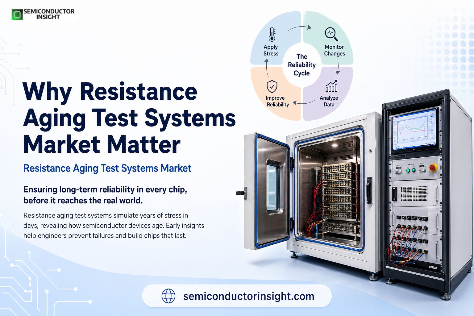
Why Resistance Aging Test Systems Market Matter Deep Inside Modern Semiconductors?
Every advanced chip that powers our phones, vehicles, data centres, and medical devices carries an invisible promise: it must perform reliably for years under varying conditions. Behind this promise lies rigorous endurance testing. Resistance aging test systems play a vital role by simulating years of real-world operation in a compressed timeframe, carefully tracking how electrical resistance changes as materials and structures age under stress.
These specialized systems apply controlled combinations of elevated temperature, voltage bias, and sometimes humidity or current loads to semiconductor devices. Engineers monitor parameters like resistance drift, leakage current, and threshold voltage shifts. Even tiny degradations can signal future problems such as electro migration in interconnects or bias temperature instability in transistors. By catching these early, manufacturers can refine designs and processes before chips reach the field.
To Stay Tuned with More meaningful and In-Depth Insights, Do Visit here: https://semiconductorinsight.com/report/resistance-aging-test-system-market/
The Physics behind the Tests
Semiconductor aging stems from multiple physical mechanisms. Negative Bias Temperature Instability (NBTI) affects PMOS transistors, causing threshold voltage increases over time. Hot Carrier Injection (HCI) damages transistors during high-energy electron flow. Electromigration moves metal atoms in tiny wires, potentially creating voids or shorts. Resistance aging test systems create accelerated conditions that speed up these processes safely, following established methodologies from organizations like JEDEC.
Standards such as JESD22-A108 for temperature, bias, and operating life provide structured frameworks. Test chambers maintain precise temperatures often between 125°C and 150°C while applying operational voltages. Devices run dynamic test patterns that toggle internal nodes, exercising the full circuit rather than simple static bias. This approach reveals weaknesses that static tests might miss.
Testing Landscape in Semiconductors
- The semiconductor industry is experiencing robust expansion, particularly in burn-in and resistance aging test systems. The burn-in test system market is estimated at $800 million in 2025 and is projected to reach $1.53 billion by 2033. Broader semiconductor test equipment follows suit, valued at $7.65 billion in 2025 and expected to grow to $12.7 billion by 2032.
- S. policy is fueling this growth through the CHIPS Act, with $30.9 billion in manufacturing awards announced in July 2025 across 40 projects and 19 companies. Meanwhile, the GaN power device market is surging from $46 million in 2020 to over $1.1 billion projected for 2026, reflecting a compound annual growth rate (CAGR) of approximately 70%.
- Reliability testing remains critical amid these advances. For instance, NBTI-induced degradation in 7nm FinFETs causes about 25% threshold voltage drift combined with hot carrier injection (HCI). Full AEC-Q100 qualification demands over 6 months, encompassing 41 tests across 7 categories with zero failures allowed.
What Shapes Current Flow in Every Circuit?
Resistance stability serves as a sensitive indicator of overall device health. As chips scale to smaller nodes, interconnects become thinner and more vulnerable. A small increase in via or line resistance can slow signal propagation or raise power consumption. Test systems equipped with high-resolution measurement capabilities detect these shifts across thousands of devices simultaneously, generating statistical confidence in long-term behavior.
In automotive and industrial applications, where chips must survive harsh environments for a decade or more, such testing becomes non-negotiable. Aerospace and medical electronics demand even stricter validation. The systems help translate laboratory data into meaningful reliability predictions, often expressed in FIT rates failures per billion device-hours.
Integration into Modern Development Flows
Today’s semiconductor teams incorporate resistance aging tests at multiple stages. During process development, they characterize new materials and transistor architectures. In qualification phases, full lots undergo extended stress to meet customer requirements. Even in high-volume manufacturing, sample testing verifies ongoing stability.
Advanced systems now offer better automation, multi-site testing, and improved data analytics. Engineers can correlate aging data with process variations, helping close the loop between fabrication and reliability. This feedback drives incremental improvements in everything from gate dielectrics to packaging materials.
A Foundation for Continued Innovation
As transistors shrink and new structures like gate-all-around devices emerge, aging behaviors grow more complex. Resistance aging test systems evolve alongside them, incorporating finer measurements and support for wider temperature ranges. They remain essential tools for turning ambitious semiconductor roadmaps into dependable products that society can trust.
- For those working at the cutting edge of electronics, these test platforms represent more than equipment they embody a commitment to endurance.
- Each carefully aged sample and recorded resistance curve contributes to chips that keep functioning long after we stop thinking about them.
- In an industry defined by constant change, the quiet discipline of aging tests helps ensure that progress remains reliable, one validated device at a time.
The ongoing refinement of these systems reflects the semiconductor community’s deep respect for time and its effects on tiny, intricate circuits. Their work behind the scenes enables the powerful, dependable technology we increasingly rely upon every day.

Comments (0)