
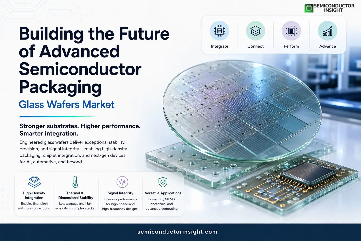
What Role Do Glass Substrates Play in 2026 Semiconductor Packaging?
Glass wafers have emerged as a strategic platform in semiconductor manufacturing, offering unique properties that address limitations of traditional silicon substrates in next-generation packaging.
Their excellent dimensional stability, smooth surface finish, and ability to support high-density through-glass vias (TGVs) make them suitable for advanced heterogeneous integration and high-performance computing applications.
Material Advantages in Semiconductor Processes
Engineered glass provides superior thermal and mechanical characteristics compared to organics in certain high-density scenarios. Its low coefficient of thermal expansion helps minimize warpage during processing of large panels or multi-layer stacks.
Manufacturers leverage glass for temporary bonding carriers during thinning and for permanent interposers that enable finer pitch interconnects. Recent demonstrations show glass core substrates handling package sizes exceeding traditional reticle limits, supporting denser silicon integration for AI accelerators.
Key Applications Driving Adoption
In image sensors and CMOS devices, glass wafers serve as transparent carriers or protective covers, enabling precise alignment and optical performance. For RF and MEMS components, the material’s low-loss dielectric properties support high-frequency signal integrity.
Emerging uses in power electronics and photonics benefit from glass’s chemical resistance and compatibility with metallization processes. Intel’s glass substrate initiatives, including demonstrations of functional devices booting operating systems, illustrate progress toward commercial AI chip packaging.
- Manufacturing and Scaling Developments
- Facilities are ramping capabilities for larger formats, moving beyond 300mm wafers toward panel-scale production for improved economies.
- Projects in India, backed by major players, target annual outputs of tens of thousands of glass substrates for 3D heterogeneous integration in defense, automotive, and computing sectors.
- These vertically integrated sites combine substrate production with assembly, aiming to strengthen local supply chains.
- Integration with Advanced Packaging Flows
- Glass interposers facilitate 2.5D and 3D stacking by providing stable platforms for chiplet placement and high-bandwidth interconnects.
- Through-glass vias allow vertical electrical connections with reduced signal loss, critical for high-performance memory and logic combinations.
- Partnerships between foundries and material suppliers focus on refining laser drilling and metallization to achieve finer pitches and higher yields.
Ongoing Global Initiatives and Case Examples
In the United States and Asia, investments support glass technology for silicon photonics and co-packaged optics, where precise alignment and thermal management are essential. European research contributes to process refinements for broader adoption.
A notable case involves facilities producing glass panels for AI workloads, where the substrate enables more efficient power delivery and heat dissipation in dense configurations.
To find out more, feel free to browse our latest updated report: https://semiconductorinsight.com/report/glass-wafers-market/
Which Suppliers Offer Structured Glass Wafers for MEMS Applications?
Several specialized manufacturers provide structured glass wafers tailored for microelectromechanical systems (MEMS) applications, where precise patterning, through-glass vias, and optical transparency are essential. Plan Optik AG stands out as a leading European supplier, offering high-precision glass wafers with custom structuring for sensors, microfluidics, and RF components. Their processes support wafer bonding and via formation suitable for integration with silicon dies in advanced MEMS packages.
- Schott AG supplies engineered glass substrates with excellent thermal stability and surface quality for MEMS pressure sensors and optical MEMS.
- Their AF32 and other borosilicate variants are widely used in wafer-level packaging due to matched coefficients of thermal expansion.
- In Asia, AGC Inc. delivers structured glass solutions for MEMS, including laser-ablated features for 3D integration in inertial sensors and biomedical devices.
- US-based companies like Corning Incorporated provide high-purity fused silica and specialty glass wafers that undergo structuring for MEMS mirrors and displays.
- Their products emphasize low autofluorescence and high flatness critical for optical MEMS. Additional players such as Nippon Electric Glass (NEG) offer alkali-free glass options structured for high-temperature MEMS processes.
These suppliers typically collaborate directly with foundries and MEMS designers to customize via densities, surface finishes, and metallization compatibility. Selection often depends on specific requirements like wafer diameter (commonly 200mm or 300mm), via aspect ratios, and hermetic sealing needs. For MEMS applications in automotive, consumer electronics, and medical devices, working with these established glass specialists ensures reliability and scalability in production.

Comments (0)