MARKET INSIGHTS
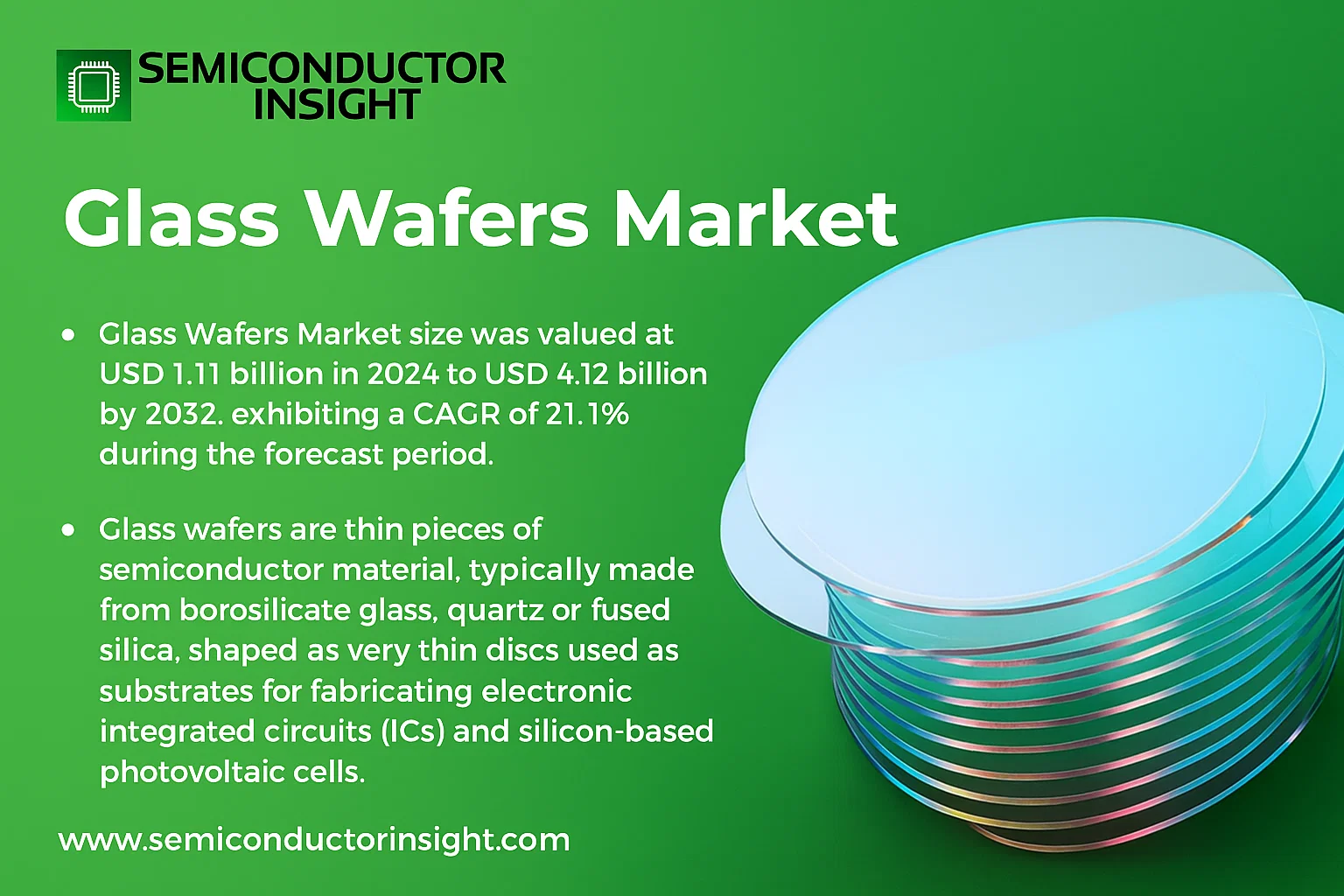
Global Glass Wafers Market size was valued at USD 1.11 billion in 2024 to USD 4.12 billion by 2032, exhibiting a CAGR of 21.1% during the forecast period.
Glass wafers are thin pieces of semiconductor material, typically made from borosilicate glass, quartz or fused silica, shaped as very thin discs used as substrates for fabricating electronic integrated circuits (ICs) and silicon-based photovoltaic cells. These wafers serve as the foundation for most microelectronic circuits and undergo multiple processes including doping, implantation and etching before the final integrated circuit product is completed.
The market is experiencing substantial growth driven by increasing demand in consumer electronics and photonics applications. Key factors propelling expansion include rising adoption in MEMS devices, growing semiconductor industry investments, and expanding applications in medical technology and automotive sectors. Furthermore, advancements in wafer-level packaging technologies and the surge in demand for high-performance computing are contributing significantly to market momentum. Major players are actively expanding their production capacities to meet growing demand; for instance, leading manufacturers like SCHOTT and Corning have recently announced facility expansions to increase their glass wafer manufacturing capabilities. SCHOTT, Nippon Electric Glass, Asahi Glass Co., and Corning represent some of the dominant companies operating in this market with comprehensive product portfolios.
MARKET DRIVERS
Proliferation of MEMS and Semiconductor Applications
The demand for glass wafers is primarily driven by their extensive use in Micro-Electro-Mechanical Systems (MEMS) and advanced semiconductor packaging. Glass wafers serve as an excellent substrate for radio frequency (RF) devices, sensors, and interposers due to their superior electrical insulation properties, thermal stability, and compatibility with silicon. The growth of the Internet of Things (IoT) and 5G technology continues to fuel the adoption of these components, creating sustained demand for high-quality glass wafers.
Advancements in Consumer Electronics and Displays
Another significant driver is the consumer electronics sector, particularly for smartphone displays, augmented reality (AR) devices, and wearables. Glass wafers are critical in the manufacturing of thin-film transistors (TFTs) and as carrier wafers for the production of flexible OLED displays. The trend toward higher resolution, bezel-less screens, and foldable devices requires the precise and robust properties that glass wafers provide.
Furthermore, the automotive industry’s shift toward electrification and advanced driver-assistance systems (ADAS) is increasing the need for sensors and electronic control units that utilize glass wafer substrates, securing a stable growth trajectory for the market.
MARKET CHALLENGES
High Manufacturing Costs and Complexity
The production of high-precision glass wafers involves sophisticated manufacturing processes, including precision grinding, polishing, and chemical strengthening. These processes require significant capital investment in equipment and cleanroom facilities. The high cost of raw materials, such as borosilicate and fused silica glass, coupled with the need for minimizing defects like surface roughness and warp, presents substantial challenges for manufacturers in maintaining competitiveness and profitability.
Other Challenges
Competition from Alternative Materials
Glass wafers face stiff competition from silicon and silicon-on-insulator (SOI) wafers in some applications, particularly where cost is a primary constraint. Silicon offers advantages in terms of established manufacturing infrastructure and thermal conductivity, which can be preferable for high-power semiconductor devices.
Supply Chain and Precision Handling
Glass wafers are inherently brittle and require specialized handling, packaging, and transportation to prevent breakage and contamination. This fragility adds complexity and cost to the supply chain, creating logistical challenges for both suppliers and end-users.
MARKET RESTRAINTS
Economic Sensitivity and Cyclical Downturns
The glass wafer market is closely tied to the health of Global semiconductor and consumer electronics industries, which are susceptible to economic cycles. During periods of economic downturn, reduced capital expenditure by major electronics manufacturers can lead to decreased orders for glass wafers. This cyclicality poses a significant restraint on consistent market growth.
Technical Limitations for Advanced Nodes
While glass wafers excel in many applications, they have limitations for the most advanced semiconductor nodes requiring extreme miniaturization. The coefficient of thermal expansion (CTE) mismatch with silicon can create integration challenges in advanced 3D IC packaging, potentially restraining their adoption in next-generation, high-performance computing applications where silicon interposers are currently dominant.
MARKET OPPORTUNITIES
Growth in Biomedical and Life Sciences
A significant growth opportunity lies in the biomedical and life sciences sectors. Glass wafers are increasingly used in biochips, microfluidic devices for lab-on-a-chip applications, and DNA sequencing. The biocompatibility, optical clarity, and chemical resistance of glass make it an ideal material for these sensitive applications, opening up new revenue streams beyond traditional electronics.
Adoption in Photonics and Optical Communication
The expansion of data centers and high-speed optical communication networks presents a major opportunity. Glass wafers are essential for manufacturing planar lightwave circuits (PLCs) and optical interconnects. The ongoing deployment of fiber-to-the-home (FTTH) and the demand for higher bandwidth are expected to drive the need for advanced photonic components built on glass substrates.
Innovations in Advanced Packaging
There is growing interest in using glass wafers as core substrates for fan-out wafer-level packaging (FOWLP) and interposers for 2.5D and 3D IC integration. Glass offers advantages in signal integrity for high-frequency applications. As the semiconductor industry pushes the limits of Moore’s Law, the role of glass in heterogeneous integration is poised to expand, creating substantial market opportunities.
Glass Wafers Market Trends
Robust Market Expansion Fueled by Semiconductor and Photovoltaic Demand
Global Glass Wafers Market, valued at USD 1110 million in 2024, is projected for significant growth, reaching USD 4117 million by 2032. This expansion, representing a Compound Annual Growth Rate (CAGR) of 21.1%, is primarily driven by the escalating demand from the semiconductor and photovoltaic industries. Glass wafers, typically made from materials like borosilicate glass, quartz, or fused silica, are essential substrates for fabricating electronic integrated circuits (ICs) and silicon-based photovoltaic cells. Their adoption is growing as the backbone for advanced microelectronic circuits, undergoing critical processes such as doping, implantation, and etching.
Other Trends
Dominance of Key Players and Global Market Concentration
The competitive landscape is characterized by a high degree of market concentration, with the top four manufacturers SCHOTT, Nippon Electric Glass, Asahi Glass Co, and Corning collectively holding over 65% of Global market share. This established dominance underscores the high barriers to entry and the significance of technological expertise and production scale in this sector.
Regional Market Leadership and Product Segmentation
Geographically, North America is the largest market, accounting for over 25% of Global share, followed closely by the combined markets of Japan and Europe, which hold over 40%. In terms of product types, 6-inch wafers constitute the largest segment, holding approximately 16% of the market. This size is favored for its balance of surface area and manufacturability across various applications.
Application Diversity and End-Use Growth
The application landscape for glass wafers is diverse. Consumer Optics represents the largest application segment, driven by demand for high-resolution displays and camera modules. This is followed by Astronomy, Industrial Equipment, Lithography, and the rapidly growing Medical & Biotech and Energy sectors, which are increasingly utilizing glass wafers for sensors, diagnostic devices, and specialized optics.
Future Outlook and Strategic Imperatives
The strong growth trajectory of the Glass Wafers Market highlights its critical role in enabling next-generation technologies. Future trends will be shaped by advancements in material science for improved thermal and chemical resistance, the miniaturization of electronic components, and the expanding need for high-precision substrates in the renewable energy sector. For companies operating in this space, the strategic focus will remain on innovation, capacity expansion, and navigating a concentrated yet highly competitive global marketplace.
COMPETITIVE LANDSCAPE
Key Industry Players
A Consolidated Market Driven by Material Science and Precision Engineering
Global Glass Wafers Market is characterized by a high degree of consolidation, with the top four manufacturers SCHOTT, Nippon Electric Glass, Asahi Glass Co., and Corning collectively commanding over 65% of the market share. This dominance is built on decades of expertise in specialty glass manufacturing, significant investment in research and development, and extensive global production and supply chain networks. These leaders provide a wide array of high-purity glass wafer substrates, including borosilicate, quartz, and fused silica, catering to demanding applications in consumer optics, astronomy, and semiconductor lithography. Their competitive strategies heavily rely on technological innovation, patent portfolios, and long-term contracts with major electronics and optics manufacturers.
Beyond the dominant leaders, the market includes several significant players who compete effectively in specific niches or regional markets. Companies like Plan Optik AG, Bullen, and Tecnisco specialize in ultra-precise manufacturing for applications such as MEMS (Micro-Electro-Mechanical Systems) and advanced packaging. Other firms, including Swift Glass, Coresix Precision Glass, and Edmund Optics, are key suppliers for prototyping and custom optics solutions, serving diverse sectors from medical technology to industrial equipment. Regional specialists like Zhejiang Lante Optics in Asia and Prazisions Glas & Optik in Europe also hold important positions, leveraging local manufacturing advantages to serve their domestic markets and global customers seeking diversified supply chains.
List of Key Glass Wafers Companies Profiled
- SCHOTT
- Nippon Electric Glass
- Asahi Glass Co.
- Corning Incorporated
- Tecnisco
- Plan Optik AG
- Bullen
- Swift Glass
- Coresix Precision Glass
- Edmund Optics
- Hoya Corporation
- Sydor Optics
- Prazisions Glas & Optik
- Valley Design
- Zhejiang Lante Optics
Segment Analysis:
| Segment Category | Sub-Segments | Key Insights |
| By Type |
|
6 inch wafers currently lead the market due to their widespread adoption in high-volume consumer applications, offering an optimal balance between manufacturing yield and functional real estate. This particular size provides a cost-effective solution for many electronic and photonic devices. Meanwhile, larger diameter wafers, such as the 12 inch segment, are anticipated to demonstrate significant growth potential, driven by the relentless pursuit of higher productivity in semiconductor fabrication facilities where maximizing the number of dies per wafer is a critical economic driver. The market also accommodates a diverse range of specialty and custom sizes to meet the specific requirements of niche applications. |
| By Application |
|
Consumer Optics represents the dominant application segment, fueled by the massive and continuous demand for smartphones, cameras, and various display technologies where glass wafers are essential for lenses, sensors, and micro-optics. The segment benefits from rapid product lifecycles and high-volume manufacturing. Following closely are the advanced requirements from the Medical & Biotech and Lithography sectors, which demand exceptionally high levels of purity, precision, and chemical resistance, often utilizing specialized materials like fused silica or quartz. The astronomy segment, while smaller, is characterized by a need for extremely large and stable substrates for high-performance telescopes and observational equipment. |
| By End User |
|
Semiconductor Manufacturers are the primary end users, leveraging glass wafers as critical substrates for integrated circuits, MEMS devices, and advanced packaging solutions. Their demand is characterized by rigorous specifications and a continuous drive for miniaturization and performance enhancement. Optoelectronic Device Makers constitute another significant segment, utilizing wafers for components like image sensors, LEDs, and optical communication devices. Research institutions drive innovation and demand for prototype and low-volume, high-specification wafers, while photovoltaic producers use them in specialized solar cell applications, and specialty fabricators serve highly customized niche markets with unique performance requirements. |
| By Material |
|
Borosilicate Glass is the leading material segment, prized for its excellent thermal shock resistance, chemical durability, and relatively low cost, making it suitable for a vast array of general electronic and consumer applications. However, Fused Silica / Quartz is essential for high-end applications requiring superior optical clarity, ultra-low thermal expansion, and high purity, such as in deep-UV lithography and high-power laser systems. The choice of material is fundamentally driven by the specific performance requirements of the end application, with soda-lime glass being used for less demanding uses and other specialty glasses developed for unique thermal, optical, or electrical properties. |
| By Manufacturing Process |
|
The Float Process is a dominant manufacturing method for producing large volumes of flat glass with excellent surface quality, which is then processed into wafers. The Fusion Draw Process is highly valued for creating substrates with pristine, fire-polished surfaces that require minimal additional finishing, making them ideal for demanding electronic and display applications. The selection of the manufacturing process is a critical determinant of the wafer’s final properties, including surface flatness, purity, and internal stress levels. Specialty fabrication techniques are employed for creating complex geometries, microstructures, or wafers with extremely tight tolerances that cannot be achieved through standard high-volume processes. |
Regional Analysis: Glass Wafers Market
The concentration of leading-edge semiconductor foundries in Taiwan, South Korea, and Japan creates massive, high-volume demand for carrier and interposer wafers. This ecosystem demands superior surface quality and thermal stability, driving local glass wafer suppliers to maintain exceptionally high-quality standards and technical expertise.
Significant investments from government bodies and private corporations fuel R&D in next-generation applications like photonic integrated circuits and advanced MEMS devices. This focus on innovation pushes the boundaries of glass wafer technology, leading to the development of wafers with enhanced optical properties and finer geometries.
The proximity to massive consumer electronics and automotive manufacturing bases ensures a steady pull for glass wafers used in image sensors, display drivers, and RF components. This close integration between suppliers and OEMs facilitates rapid technology adoption and customization of wafer specifications.
A mature and highly efficient supply chain for high-purity silica and specialty glasses supports the manufacturing base. Local expertise in material science and precision engineering allows for cost-effective production of high-performance wafers, giving the region a distinct advantage in both quality and scalability.
North America
North America maintains a strong position in the Glass Wafers Market, characterized by a focus on high-value, specialized applications. The region is a leader in sectors requiring advanced R&D, such as aerospace, defense, and biomedical devices, where glass wafers are used for specialized sensors, optical components, and lab-on-a-chip technologies. The presence of major technology companies and research institutions drives demand for high-performance wafers with unique properties, like extreme chemical durability or specific optical transmission. While the volume may be lower than in Asia-Pacific, the emphasis is on cutting-edge innovation and applications with high technical barriers, supporting a robust niche market for specialized glass wafer manufacturers.
Europe
Europe’s glass wafer market is mature and technology-driven, with strength in automotive, industrial, and telecommunications applications. The region’s strong automotive industry, particularly in Germany, demands glass wafers for various sensors and lighting systems. Furthermore, European companies are pioneers in environmental and industrial sensing technologies, which utilize glass substrates for their stability and reliability. A well-established research infrastructure supports innovation in photonics and MEMS, fostering demand for high-quality wafers. The market is characterized by a focus on precision, quality, and adherence to stringent regulatory standards, catering to high-value industrial and technological sectors.
South America
The glass wafer market in South America is nascent but developing, with growth primarily linked to regional electronics assembly operations and gradual technological adoption. Brazil is the most significant market, with demand driven by the automotive and consumer electronics sectors. The market is largely served by imports, but there is growing interest in establishing local capabilities to support regional manufacturing. Growth is incremental, tied to broader economic stability and increasing investment in local technology infrastructure, focusing on mid-range applications rather than leading-edge technologies.
Middle East & Africa
The Middle East & Africa region represents an emerging market with potential tied to strategic investments in diversification. Gulf Cooperation Council countries, in particular, are investing in technology and industrial sectors as part of long-term economic visions, which could spur future demand for components like glass wafers. Currently, the market is small and import-dependent, with limited local manufacturing. Growth is expected to be slow and linked to the development of downstream electronics and semiconductor-related industries, with a focus on serving regional needs for communication infrastructure and consumer goods.
Report Scope
This market research report provides a comprehensive analysis of the Glass Wafers Market, covering the forecast period 2025–2032. It offers detailed insights into market dynamics, technological advancements, competitive landscape, and key trends shaping the industry.
Key focus areas of the report include:
- Market Overview: The report begins with an overview outlining its current market scenario, key growth indicators, and industry transformation drivers. It discusses macroeconomic factors, demand–supply balance, regulatory landscape, and the strategic role of semiconductors in powering advancements across industries such as automotive, telecommunications, consumer electronics, and industrial automation.
- Market Size & Forecast: Historical data and future projections for revenue, unit shipments, and market value across major regions and segments.
- Segmentation Analysis: Detailed breakdown by product type, technology, application, and end-user industry to identify high-growth segments and investment opportunities.
- Regional Insights: Insights into market performance across North America, Europe, Asia-Pacific, Latin America, and the Middle East & Africa, including country-level analysis where relevant.
- Competitive Landscape: Profiles of leading market participants, including their product offerings, R&D focus, manufacturing capacity, pricing strategies, and recent developments such as mergers, acquisitions, and partnerships.
- Technology Trends & Innovation: Assessment of emerging technologies, integration of AI/IoT, semiconductor design trends, fabrication techniques, and evolving industry standards.
- Market Drivers & Restraints: Evaluation of factors driving market growth along with challenges, supply chain constraints, regulatory issues, and market-entry barriers.
- Stakeholder Insights: Insights for component suppliers, OEMs, system integrators, investors, and policymakers regarding the evolving ecosystem and strategic opportunities.
Primary and secondary research methods are employed, including interviews with industry experts, data from verified sources, and real-time market intelligence to ensure the accuracy and reliability of the insights presented.
FREQUENTLY ASKED QUESTIONS:
What is the current market size of Glass Wafers Market?
-> Glass Wafers Market size was valued at USD 1.11 billion in 2024 to USD 4.12 billion by 2032, exhibiting a CAGR of 21.1% during the forecast period.
Which key companies operate in Glass Wafers Market?
-> Key players include SCHOTT, Nippon Electric Glass, Asahi Glass Co, and Corning, among others. Global top four manufacturers hold a combined market share of over 65%.
What are the key growth drivers?
-> Key growth drivers include advancements in semiconductor fabrication, increasing demand for electronic integrated circuits (ICs) and silicon-based photovoltaic cells, and the expanding applications in consumer optics and industrial equipment.
Which region dominates the market?
-> North America is the largest market, with a share of over 25%, followed by Japan and Europe, which together hold over 40% of the market share.
What are the emerging trends?
-> Emerging trends include the adoption of larger wafer sizes like 6 inch, technological innovations in doping and etching processes, and growing applications in medical & biotech and energy sectors.

Get Sample Report PDF for Exclusive Insights
Report Sample Includes
- Table of Contents
- List of Tables & Figures
- Charts, Research Methodology, and more...


