
What Is Changing Inside the 300 mm Wafer FOUP and FOSB Market as Advanced Nodes Scale?
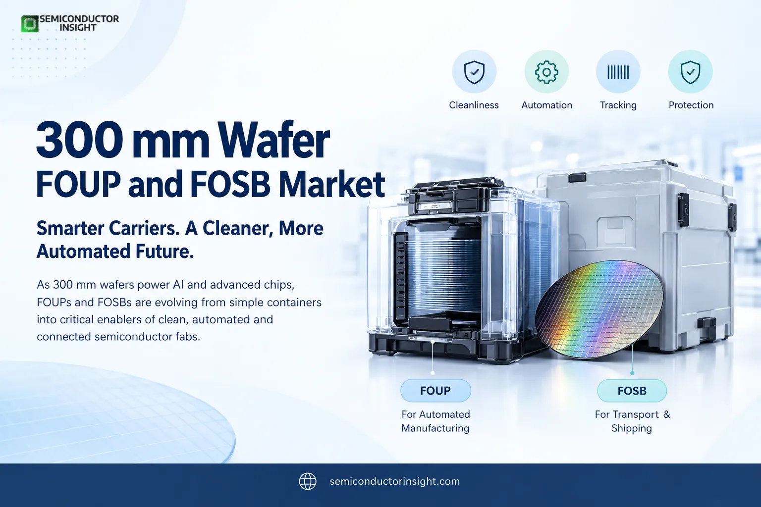
Inside a modern semiconductor fab, a 300 mm wafer may travel through hundreds of process steps before becoming part of a finished chip. The container carrying it is therefore much more than packaging. Front Opening Unified Pods (FOUPs) and Front Opening Shipping Boxes (FOSBs) are becoming integral to wafer cleanliness, automated handling, identification and damage prevention.
The scale of the underlying ecosystem is substantial. Global semiconductor manufacturing capacity is projected to reach 11.1 million 300 mm-equivalent wafers per month by 2028, while capacity for 7 nm and below is expected to rise from about 850,000 wafers per month in 2024 to 1.4 million by 2028.
Why 300 mm Is Changing the Logistics Equation?
- A 300 mm wafer has twice the diameter of a 200 mm wafer, but the usable surface area is substantially larger. That makes each wafer capable of carrying more dies, improving manufacturing efficiency for high-volume devices such as processors, memory and advanced logic.
- The latest shipment figures reinforce this shift. Worldwide silicon wafer shipments reached 3,275 million square inches in the first quarter of 2026, up 13.1% year over year. Industry reporting specifically linked continuing strength to AI data centers, advanced logic, memory and power-management devices.
- More wafer movement means more opportunities for contamination, mechanical damage and handling errors, placing greater importance on the carrier surrounding every wafer batch.
FOUP and FOSB Have Different Jobs
The distinction between the two formats is becoming increasingly important as semiconductor logistics become more automated.
A FOUP is designed for use within automated semiconductor manufacturing environments. It interfaces with fab equipment and material-handling systems while maintaining a controlled environment around the wafers. FOSB, by comparison, is designed primarily for transporting and shipping 300 mm wafers between wafer suppliers and semiconductor manufacturers.
The SEMI M31 specification describes FOSB as a shipping container intended to maintain wafer quality during transportation and recommends automated transfer from the FOSB into a FOUP, FOBIT or open cassette before manufacturing operations.
The Journey of a 300 mm Wafer Is Becoming More Automated
The modern material-flow sequence increasingly resembles a closed logistics loop:
Wafer Manufacturing
↓
Inspection
↓
FOSB Protection
↓
Inter-Facility Transport
↓
Receiving and Verification
↓
Automated Wafer Transfer
↓
FOUP Loading
↓
AMHS Movement
↓
Process Equipment
↓
Inspection and Rework
This architecture reduces manual intervention and allows fabs to connect wafer movement with automated material-handling systems.
AI Is Increasing the Value of Every Clean Wafer Move
The current AI semiconductor expansion is creating a particularly important environment for 300 mm carriers. Advanced logic and high-bandwidth memory require extremely controlled manufacturing conditions, while wafer suppliers and chipmakers continue expanding capacity.
In the second quarter of 2026, worldwide silicon wafer shipments reached 3,573 million square inches, 7.4% higher than the same quarter of 2025. The industry attributed growth to AI demand extending beyond advanced logic and memory into power devices and photonics.
For FOUP and FOSB suppliers, this translates into a requirement for consistent dimensional accuracy, cleanliness, reliable door interfaces and compatibility with increasingly automated fabs.
Standards Are Quietly Shaping Carrier Design
Carrier design is closely connected with semiconductor manufacturing standards. SEMI E62 addresses features associated with 300 mm front-opening interfaces, while SEMI M31 establishes mechanical requirements for FOSBs used to transport and ship 300 mm wafers.
That standardization is important because wafers can move between different manufacturing facilities, equipment platforms and logistics environments. Interchangeability reduces friction when fabs scale production or introduce additional automation.
You can freely browse our most recent updated report to learn more about it before scrolling further: https://semiconductorinsight.com/report/300-mm-wafer-foup-and-fosb-market/
The New Requirement Is Not Simply Protection
The next stage of the 300 mm Wafer FOUP and FOSB Market is increasingly connected to digital manufacturing. A carrier needs to support physical protection while fitting into automated identification, tracking and material-flow systems.
The direction is becoming clear: cleaner containers, more precise interfaces, fewer manual touches and stronger compatibility with automated handling. As advanced semiconductor production expands, FOUPs and FOSBs are becoming a quiet but essential layer of the industry’s manufacturing infrastructure.

Comments (0)