
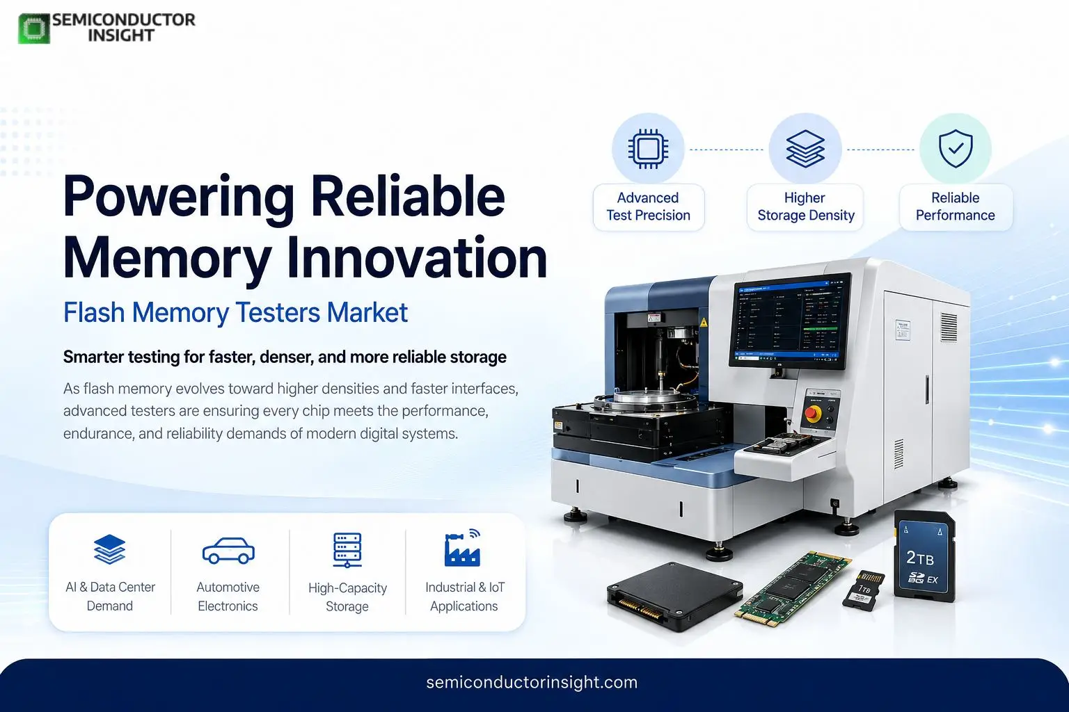
Wafer Testing vs. Final Package Testing in the Flash Memory Testers Market Complete Comparison
As AI infrastructure, automotive electronics, and high-capacity storage devices continue to scale, flash memory testers have become one of the most critical technologies ensuring that every memory chip delivers the speed, endurance, and reliability demanded by modern digital systems.
Flash memory has evolved from powering simple USB drives to becoming the foundation of smartphones, cloud computing, AI servers, autonomous vehicles, industrial automation, and consumer electronics. Every NAND flash chip manufactured today undergoes extensive electrical and functional testing before reaching an end product. This growing complexity has elevated flash memory testers from production equipment to strategic quality assurance systems capable of validating billions of memory cells in increasingly dense semiconductor architectures. With manufacturers producing higher-layer 3D NAND devices and transitioning toward more sophisticated packaging technologies, testing precision has become just as important as fabrication itself.
Looking Beyond Revenue to Understand the Flash Memory Testers Market
- Rather than evaluating the flash memory testers market solely through financial estimates, its growth is better reflected through semiconductor production volumes, storage capacity trends, and testing complexity.
- Modern 3D NAND flash devices now exceed 300 memory layers, compared with fewer than 40 layers a decade ago. A single enterprise solid-state drive can store 30 TB or more, while advanced data center SSDs continue moving toward 60 TB capacities.
- According to industry publications and manufacturer announcements, global semiconductor fabs process millions of memory wafers annually, with every wafer requiring multiple electrical and reliability inspections before packaging.
- Each NAND wafer contains thousands of individual memory dies, and every die must be screened for programming accuracy, endurance, read/write performance, retention characteristics, and defect mapping. As storage densities increase, testing times, automation requirements, and data analysis capabilities also expand significantly.
Why Memory Testing Is Becoming Smarter Than Memory Manufacturing?
Semiconductor manufacturers are no longer focused only on detecting defective chips. Modern flash memory testers analyze signal integrity, latency consistency, endurance cycles, thermal behavior, power consumption, and error correction performance simultaneously.
Artificial intelligence is increasingly assisting automated test equipment by identifying subtle manufacturing variations before they affect final yields. Machine learning algorithms can evaluate enormous datasets generated during wafer probing and final package testing, allowing engineers to optimize manufacturing processes while reducing false failures.
Recent announcements from leading automated test equipment manufacturers highlight continued investment in high-speed testers capable of supporting PCIe Gen5 and Gen6 SSD controllers, UFS mobile storage, and next-generation automotive memory devices.
From Wafer to Memory Card Where Testing Happens
Silicon Wafer Fabrication
│
▼
Memory Cell Formation
│
▼
Wafer Probe Testing
│
▼
Die Separation
│
▼
Package Assembly
│
▼
Final Functional Testing
│
▼
SSD Memory Card USB Drive Smartphone
Testing occurs repeatedly throughout manufacturing because defects can appear at different stages, from wafer fabrication to final packaging.
How EEPROM Relates to Flash Memory and Memory Sticks?
- Although EEPROM (Electrically Erasable Programmable Read-Only Memory) and flash memory belong to the same family of non-volatile memory technologies, they serve different purposes. EEPROM allows data to be erased and rewritten one byte at a time, making it ideal for storing configuration settings, firmware parameters, calibration data, and embedded system information. Flash memory, by contrast, erases data in blocks or sectors, enabling much higher storage densities and faster operation for mass-storage applications.
- This architectural difference explains why EEPROM is commonly found in automotive control units, industrial sensors, networking equipment, and embedded microcontrollers, while flash memory dominates SSDs, USB flash drives, smartphones, digital cameras, and memory cards.
- Today’s consumer USB flash drives commonly range from 32 GB to 1 TB, while SD Express memory cards are reaching capacities of 2 TB under the latest standards. Enterprise SSDs now exceed 60 TB, demonstrating how block-based flash technology has become the preferred architecture for high-capacity storage.
- Because EEPROM and flash memory share similar floating-gate transistor principles, many semiconductor test platforms support validation of both technologies. Testers evaluate programming voltage, erase cycles, retention time, read margins, and endurance performance to ensure reliable long-term operation. Many EEPROM devices are designed to withstand 100,000 to 1 million write/erase cycles, while NAND flash endurance varies depending on SLC, MLC, TLC, QLC, or PLC architectures.
To find out more, feel free to browse our latest updated report: https://semiconductorinsight.com/report/flash-memory-testers-market/
Current Industry Momentum
Several developments continue reshaping flash memory testing worldwide. AI servers equipped with massive SSD arrays are increasing demand for enterprise-grade NAND validation. Major manufacturers including Samsung Electronics, Kioxia, Micron Technology, SK hynix, and Western Digital continue advancing high-layer NAND technologies, requiring more sophisticated automated testing solutions.
The rapid expansion of AI data centers, edge computing, automotive electronics, and industrial IoT devices means storage reliability is becoming a mission-critical requirement. As memory architectures continue evolving toward higher densities and faster interfaces, flash memory testers will remain one of the most essential technologies ensuring the quality, reliability, and long-term performance of the world’s digital storage infrastructure.

Comments (0)