Ultra Fast Pulse Innovation Reshaping Semiconductor Sub-nanosecond passively Q-switched microchip lasers Systems
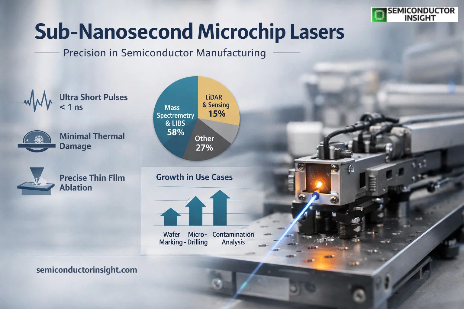
Sub-nanosecond passively Q-switched microchip lasers are emerging as one of the most critical photonics tools in semiconductor fabrication and precision analytics. These compact, solid-state laser systems generate extremely short pulses often below 1 nanosecond allowing engineers to perform high-resolution material processing with minimal thermal damage. As chip architectures shrink below 5 nm and advanced packaging becomes mainstream, the role of such lasers is becoming more central rather than complementary.
How Pulse Physics Enables Semiconductor Precision?
The working principle of these lasers is based on passive Q‑switching, in which a saturable absorber typically Cr: YAG or a semiconductor‑based absorber modulates the intracavity losses to generate intense, short light pulses. The emitted pulses can achieve durations as low as 489 picoseconds, with peak power exceeding 45 kW, highlighting the capability of these systems to deliver high optical energy within extremely short time intervals.
In semiconductor processing, this translates into:
- Precise wafer scribing without thermal diffusion
- Controlled ablation for thin film removal
- Minimal microcrack formation in brittle substrates like silicon carbide
The chemical and physical advantage is clear shorter pulses reduce heat-affected zones, preserving crystal integrity.
Tap into the Latest Trends from Our Recent Study: https://semiconductorinsight.com/report/8-inch-rapid-annealing-furnace-market/
Semiconductor Innovation Powering Industry Growth Trends
A significant portion of this demand comes from semiconductor and analytical instrumentation sectors, where:
- Mass spectrometry and LIBS together contribute over 55-60% of total application demand
- Lidar and sensing technologies are rapidly expanding, holding around 15% share with strong future potential
This growth aligns with the increasing need for defect-free chip fabrication and high-throughput inspection tools.
Material Engineering Driving Laser Efficiency
The performance of sub-nanosecond microchip lasers depends heavily on material selection. Rare-earth doped crystals such as Nd:YAG, Nd:GdVO₄, and Nd:LuAG are commonly used as gain media, while saturable absorbers like Cr⁴⁺:YAG or semiconductor saturable absorber mirrors (SESAMs) regulate pulse formation.
Recent research is also exploring:
- Graphene and 2D materials for ultra-fast switching
- CMOS-compatible photonic integration for chip-scale lasers
- Ceramic laser media for higher thermal stability
These advancements are enabling compact laser modules with footprints as small as a few millimeters, ideal for integration into semiconductor tools.
Product Landscape across Industrial Applications
The product ecosystem is diverse, tailored for different precision requirements in semiconductor and analytical industries.
Single-mode microchip lasers dominate high-precision applications due to superior beam quality, accounting for nearly 65% of usage share.
Multi-mode lasers, on the other hand, are preferred in cost-sensitive or high-energy applications where beam quality is slightly relaxed.
Key product types include:
- Diode-pumped solid-state microchip lasers
- Nd:YAG passively Q-switched micro lasers
- Fiber-coupled microchip laser modules
- Compact integrated photonic micro lasers
Each product is engineered for specific use cases such as wafer inspection, micromachining, or spectroscopy.
Top Brands Shaping the Competitive Ecosystem
The competitive landscape is defined by highly specialized photonics companies focusing on precision engineering and semiconductor integration.
Leading global brands include:
- Alphalas
- CryLaS
- Novanta Photonics
- RPMC Lasers
- Tokyo Instruments
- Standa
These companies are actively investing in miniaturization, energy efficiency, and integration with semiconductor fabrication equipment.
Semiconductor Use Cases Expanding Beyond Lithography
While traditional lithography relies on excimer lasers, sub-nanosecond microchip lasers are gaining ground in niche but critical semiconductor processes.
Emerging use cases include:
- Wafer marking and traceability systems
- Micro-drilling in advanced packaging
- Laser-induced breakdown spectroscopy for contamination detection
- Precision trimming of electronic components
Their ability to operate with high repetition rates and stable output makes them ideal for inline production environments.
Next Phase Driven by Integration and Miniaturization
Deeper integration with semiconductor manufacturing systems is key to this market’s development. With pulse energies surpassing 150 nJ in small footprints under 10 mm², chip-scale lasers compatible with CMOS platforms are now being demonstrated, indicating a move toward fully integrated photonic systems.
As semiconductor nodes continue shrinking and heterogeneous integration becomes the norm, these lasers will move from standalone tools to embedded components within fabrication ecosystems.
In essence, sub-nanosecond passively Q-switched microchip lasers are not just enabling precision they are redefining how precision is achieved in the semiconductor era.
Comments (0)