Market Insights
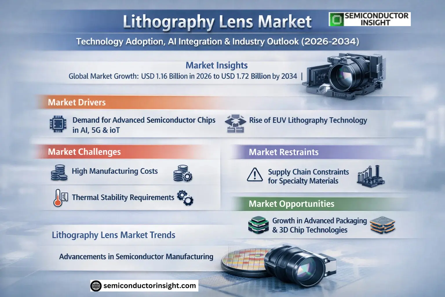
Global Lithography Lens Market size was valued at USD 1.09 billion in 2025. The market is projected to grow from USD 1.16 billion in 2026 to USD 1.72 billion by 2034, exhibiting a CAGR of 6.9% during the forecast period.
Lithography lenses are critical optical components used in semiconductor manufacturing and other precision industries to project patterns onto silicon wafers with nanometer-scale accuracy. These high-precision lenses utilize advanced materials and coatings to minimize aberrations, enabling the production of smaller, more efficient microchips. The technology is categorized into deep ultraviolet (DUV) and extreme ultraviolet (EUV) lithography lenses, each serving different node requirements in chip fabrication.
Market growth is driven by increasing demand for advanced semiconductor devices, particularly in artificial intelligence, 5G networks, and IoT applications. While DUV lenses currently dominate the market due to their cost-effectiveness for mature nodes, EUV adoption is accelerating for cutting-edge sub-7nm processes. Key players like Carl Zeiss and Nikon continue to innovate lens designs to support shrinking transistor sizes, though supply chain challenges for specialized glass materials remain a constraint.
MARKET DRIVERS
Increasing Demand for Advanced Semiconductor Chips
Lithography Lens Market is experiencing growth due to the rising demand for high-performance semiconductor chips in AI, 5G, and IoT applications. Leading manufacturers are investing heavily in advanced lithography lens systems to achieve nanometer-scale precision in chip fabrication. Global semiconductor industry’s projected 8% annual growth further accelerates this demand.
Technological Advancements in EUV Lithography
Extreme Ultraviolet (EUV) lithography systems require highly specialized lenses capable of handling 13.5nm wavelength light. With EUV adoption increasing to over 40% of leading-edge chip production, the demand for precision lithography lenses has surged. This technology enables smaller transistor sizes and higher chip densities, driving market expansion.
Government initiatives supporting domestic semiconductor manufacturing in regions like North America and Europe are creating additional demand for lithography lens systems.
MARKET CHALLENGES
High Manufacturing Complexity and Costs
Lithography lenses require flawless optical perfection with surface irregularities measured in picometers, making production exceptionally challenging. A single EUV lithography lens system can cost over USD 50 million, creating significant barriers to market entry and technology adoption.
Other Challenges
Thermal Stability Requirements
Maintaining nanometer-level precision across temperature fluctuations requires exotic materials and sophisticated cooling systems, adding to development costs and technical complexity in the Lithography Lens Market.
MARKET RESTRAINTS
Supply Chain Constraints for Specialty Materials
Lithography Lens Market faces constraints from limited availability of high-purity fused silica and calcium fluoride crystals essential for lens manufacturing. With fewer than five global suppliers capable of meeting semiconductor-grade standards, material shortages periodically disrupt production schedules and limit market growth.
MARKET OPPORTUNITIES
Emerging Applications in Advanced Packaging
The shift towards 3D chiplet architectures and advanced packaging technologies is creating new opportunities for lithography lens manufacturers. Fan-out wafer-level packaging and through-silicon via applications require specialized lithography solutions, opening a USD 420 million adjacent market for lens systems by 2026.
Lithography Lens Market Trends
Advancements in Semiconductor Manufacturing Drive Demand
Lithography Lens Market is experiencing significant growth due to increasing demand for advanced semiconductor manufacturing. As chip manufacturers push for smaller node sizes, the precision requirements for lithography lenses have intensified. Industry leaders like Carl Zeiss and Nikon continue to invest heavily in developing lenses with higher numerical apertures and reduced aberrations to meet these demands.
Other Trends
Transition to EUV Lithography Technology
The shift from DUV to EUV lithography systems represents a key trend, with EUV lithography lenses requiring more sophisticated optical designs. This transition is driving innovation in lens materials and coatings to handle extreme ultraviolet wavelengths while maintaining high transmission rates and minimizing thermal distortion.
Regional Market Developments
Asia-Pacific, particularly China and South Korea, is emerging as a major growth region for lithography lenses due to expanding semiconductor fabrication facilities. Meanwhile, established markets like the U.S. and Germany continue to lead in advanced R&D and high-end lens production.
Increasing Competition Among Key Manufacturers
The market is witnessing intensified competition among major players, with companies focusing on proprietary lens designs and manufacturing techniques. Strategic partnerships between lens manufacturers and semiconductor equipment providers are becoming more common to develop integrated lithography solutions.
Supply Chain Optimization Efforts
Manufacturers are increasingly focusing on supply chain resilience, with efforts to localize critical component production and reduce lead times. This includes developing domestic sources for specialized optical materials and precision mechanical components used in high-end lithography lenses.
COMPETITIVE LANDSCAPE
Key Industry Players
Technological Innovation Drives Market Leadership in Precision Optics
Carl Zeiss AG dominates the Lithography Lens Market with approximately 40% revenue share, leveraging its pioneering EUV lens systems for advanced semiconductor nodes. The German optics specialist maintains technological superiority through strategic partnerships with ASML and sustained R&D investments exceeding 15% of annual revenue. Nikon and Canon follow as established Japanese competitors, collectively holding 30-35% market share, though their DUV lens portfolios face margin pressures from Chinese manufacturers.
Emerging Chinese players like Nanjing Wavelength Opto-Electronic and Shenzhen Canrill Technologies are gaining traction in mid-range DUV applications, supported by government semiconductor initiatives. Specialized firms such as Jenoptik and Oceana Optics focus on customized solutions for niche optoelectronic applications, while Taiwanese manufacturers like Largan Precision are expanding into wafer-level packaging lenses. The market exhibits moderate concentration with the top 5 players controlling nearly 75% of global revenue.
List of Key Lithography Lens Companies Profiled
- Carl Zeiss AG
- Nikon Corporation
- Canon Inc.
- Nanjing Wavelength Opto-Electronic Science & Technology
- Shenzhen Canrill Technologies
- Hefei Bohu Optoelectronic Technology
- Jenoptik AG
- Oceana Optics Inc.
- Largan Precision Co.
- Union Optoelectronics
- SUSS MicroOptics
- Physik Instrumente GmbH
- OptoSigma Corporation
- SCHOTT AG
- Edmund Optics
Segment Analysis:
| Segment Category | Sub-Segments | Key Insights |
| By Type |
|
EUV Lithography Lens represents the technological frontier in lithography optics with superior precision capabilities:
|
| By Application |
|
Semiconductor Manufacturing dominates application demand due to:
|
| By End User |
|
Foundries represent the most technically demanding end-users:
|
| By Technology Node |
|
≤7nm nodes demonstrate most aggressive requirements:
|
| By Manufacturing Stage |
|
Front-End Processing accounts for majority of high-value lens usage:
|
Regional Analysis: Global Lithography Lens Market
Taiwan and South Korea lead in adopting cutting-edge EUV lithography lenses, with advanced nodes below 5nm driving replacement cycles. Japanese manufacturers maintain leadership in high-precision optical materials crucial for next-generation lenses.
The region benefits from a dense network of specialized component suppliers, including precision glass manufacturers and coating specialists. This integrated supply chain reduces lead times and supports rapid technology iterations in lithography lens production.
National semiconductor policies across APAC countries provide incentives for equipment upgrades. Japan’s focus on semiconductor material sovereignty and China’s import substitution programs create favorable conditions for domestic lithography lens adoption.
Leading Asian research institutions collaborate with lens manufacturers on thermal stability solutions and aberration correction technologies. These partnerships accelerate innovations in lithography lens performance for smaller node production.
North America
North America maintains strong lithography lens demand driven by leading semiconductor equipment manufacturers and advanced R&D facilities. The region hosts key innovation centers for EUV technology development, with major OEMs collaborating closely with research universities on next-generation lens designs. Domestic semiconductor reshoring initiatives create new opportunities for lithography lens suppliers, particularly for mature nodes. The presence of AI chip designers and advanced packaging facilities generates additional demand for specialized lithography solutions.
Europe
Europe’s Lithography Lens Market benefits from strong automotive and industrial semiconductor sectors. Leading optical companies provide specialized lenses for niche applications including MEMS and power devices. Collaborative R&D programs between EU member states focus on developing alternative lithography technologies. The region maintains particular strength in metrology-grade lens systems for semiconductor quality control applications.
Middle East & Africa
Emerging semiconductor initiatives in the Middle East are creating new opportunities for lithography lens adoption, particularly for legacy node production. Government-backed technology diversification programs aim to develop local semiconductor manufacturing capabilities. Strategic partnerships with Asian and European lens manufacturers help bridge the technology gap in these developing markets.
South America
South America’s Lithography Lens Market remains in early development stages, focused mainly on supporting regional electronics manufacturing. Limited domestic semiconductor production keeps lens demand concentrated on maintenance and replacement cycles. However, increasing investments in technology parks and special economic zones show potential for future market expansion.
Report Scope
This market research report provides a comprehensive analysis of the Lithography Lens Market, covering the forecast period 2025–2034. It offers detailed insights into market dynamics, technological advancements, competitive landscape, and key trends shaping the industry.
Key focus areas of the report include:
- Market Overview: The report begins with an overview outlining its current market scenario, key growth indicators, and industry transformation drivers. It discusses macroeconomic factors, demand–supply balance, regulatory landscape, and the strategic role of lithography lenses in powering advancements across industries such as semiconductor manufacturing, optoelectronic components, and others.
- Market Size & Forecast: Historical data and future projections for revenue, unit shipments, and market value across major regions and segments.
- Segmentation Analysis: Detailed breakdown by product type, technology, application, and end-user industry to identify high-growth segments and investment opportunities.
- Regional Insights: Insights into market performance across North America, Europe, Asia-Pacific, Latin America, and the Middle East & Africa, including country-level analysis where relevant.
- Competitive Landscape: Profiles of leading market participants, including their product offerings, R&D focus, manufacturing capacity, pricing strategies, and recent developments such as mergers, acquisitions, and partnerships.
- Technology Trends & Innovation: Assessment of emerging technologies, integration of AI/IoT, lithography lens design trends, fabrication techniques, and evolving industry standards.
- Market Drivers & Restraints: Evaluation of factors driving market growth along with challenges, supply chain constraints, regulatory issues, and market-entry barriers.
- Stakeholder Insights: Insights for component suppliers, OEMs, system integrators, investors, and policymakers regarding the evolving ecosystem and strategic opportunities.
Primary and secondary research methods are employed, including interviews with industry experts, data from verified sources, and real-time market intelligence to ensure the accuracy and reliability of the insights presented.
FREQUENTLY ASKED QUESTIONS:
What is the current market size of Lithography Lens Market?
-> Lithography Lens Market size was valued at USD 1.09 billion in 2025. The market is projected to grow from USD 1.16 billion in 2026 to USD 1.72 billion by 2034, exhibiting a CAGR of 6.9% during the forecast period.
Which key companies operate in Lithography Lens Market?
-> Key players include Carl Zeiss, Nikon, Canon, Nanjing Wavelength Opto-Electronic Science & Technology, Shenzhen Canrill Technologies, and Hefei Bohu Optoelectronic Technology, among others.
What are the key growth drivers?
-> Key growth drivers include rising demand for semiconductor manufacturing, advancements in lithography technology, and increasing investments in optoelectronic components.
Which region dominates the market?
-> Asia is the fastest-growing region, with China showing significant market potential, while North America and Europe remain key markets.
What are the emerging trends?
-> Emerging trends include development of EUV lithography lenses, precision optics advancements, and integration with next-generation semiconductor fabrication technologies.
Get Sample Report PDF for Exclusive Insights
Report Sample Includes
- Table of Contents
- List of Tables & Figures
- Charts, Research Methodology, and more...
 Download Sample Report PDF