

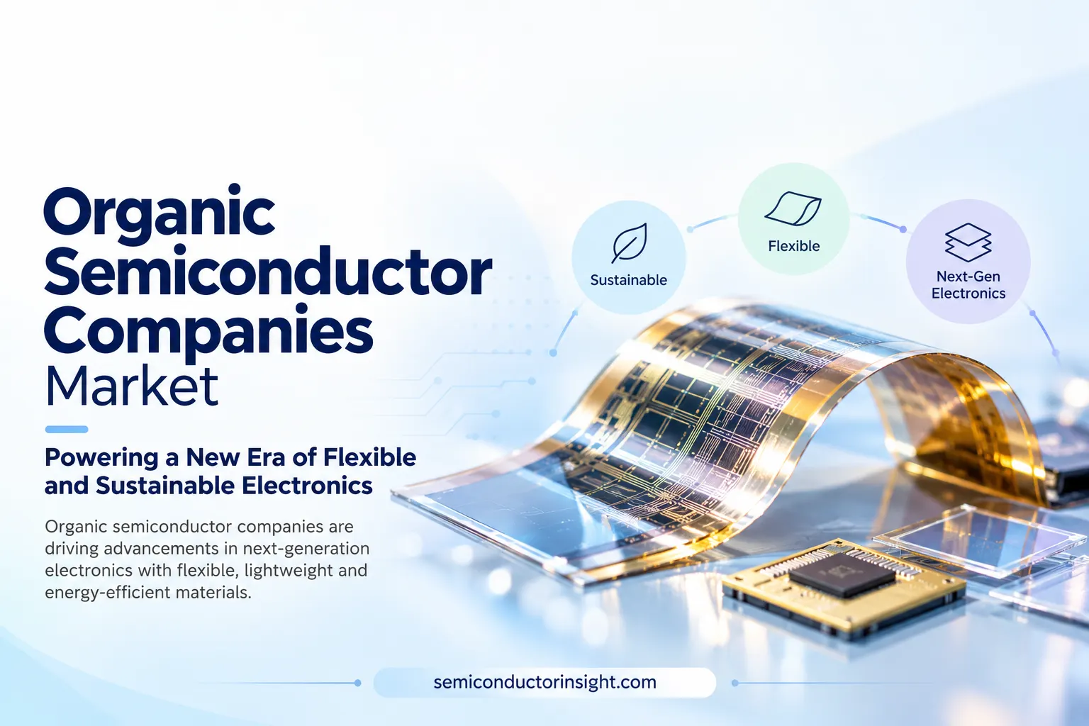
Top 10 Organic Semiconductor Companies Shaping the Future of Wearable Electronics and Organic Photovoltaics
The organic semiconductor space in 2026 is defined by phosphorescent emitters powering brighter, more efficient OLED stacks, Gen 8.6 substrate lines unlocking larger IT panels, and flexible organic photovoltaics finding real-world surfaces that silicon cannot reach.
Panel makers are racing to fill new capacity while materials specialists push blue efficiency and lifetime gains that reshape power budgets across phones, laptops, and vehicles. Here is a closer look at the companies shaping that reality right now.
Universal Display Corporation
Phosphorescent OLED materials from this specialist remain the backbone of high-efficiency red and green emission layers across nearly every major panel maker. By mid-2026 the company held more than 7,000 patents issued and pending worldwide, giving it unmatched leverage in the emissive stack. Customers including Samsung Display, BOE, LG Display, Visionox and TCL CSOT continued multi-year material supply relationships as new Gen 8.6 fabs began consuming larger volumes.
Technical progress on phosphorescent blue delivered lifetime improvements measured at 13 times earlier benchmarks and energy-efficiency gains that can reach 25% once fluorescent blue is fully replaced. LG Display already demonstrated a 15% efficiency lift in commercial-style devices. With more than $20 billion committed industry-wide to Gen 8.6 capacity and the first lines from Samsung and BOE entering mass production in summer 2026, material demand is shifting from smartphone-centric to IT and automotive volumes. Universal Display’s vapor-jet printing platform also advanced, supporting digitally patterned deposition suitable for 4K and 8K resolutions on flexible substrates.
Samsung Display
The industry’s first Gen 8.6 OLED line reached mass production in early 2026 at the Asan campus, initially running one 7,500-substrate-per-month line that later scaled toward the full 15,000-substrate design capacity. Yields climbed past 90% within weeks of ramp, enabling early shipments of 14-inch and 16-inch panels destined for premium notebook designs. The $3.1 billion-scale investment targets IT applications where OLED penetration still sits in the single digits.
Parallel progress on LTPO+ backplanes and tandem architectures continues to feed Apple’s premium smartphone and foldable roadmaps, with production volumes for the latest Pro series modules measured in the tens of millions of units. The larger mother-glass size allows more laptop and tablet panels per substrate than previous Gen 6 lines, cutting unit costs while supporting higher refresh rates and brightness levels required by AI-PC and creative-workstation markets.
LG Display
Large-area white OLED and RGB tandem structures remain the company’s strength, with gaming-monitor panel yields now reported in the mid-90% range. Monitor panels are projected to account for roughly 20% of large OLED shipments in 2026, roughly double the prior year’s share. An additional Gen 6 line investment of about 1.1 trillion won is under way at the Paju complex to expand capacity for IT and mobile applications while validating next-generation mask-free processes.
Shipments of premium smartphone panels continue in the high tens of millions of units annually, and the company is accelerating conversion work on existing Gen 8 white-OLED capacity toward eLEAP-style RGB production aimed at larger IT formats. These moves keep LG Display central to high-end television, monitor, and emerging automotive organic-display demand.
BOE Technology
China’s first Gen 8.6 AMOLED line at the Chengdu B16 facility began commercial mass production in June 2026 after a 63-billion-yuan investment. Designed for 32,000 substrates per month, the line produces tandem LTPO panels supporting 1-240 Hz variable refresh and is already shipping 14-inch 2.8K notebook panels to multiple IT brands. More than ten device makers attended the launch event, confirming early demand from the notebook and tablet segment.
The facility is the first high-generation Chinese line to support both flexible and hybrid OLED processes on the same platform. Combined with existing Gen 6 flexible capacity across the Sichuan-Chongqing region, BOE has now shipped cumulative OLED volumes exceeding 600 million units, positioning it as a volume force in the expanding mid-size organic-display market.
For More Detailed Insights, You Can Surf Our Latest Report Here: https://semiconductorinsight.com/report/organic-semiconductor-market/
TCL CSOT
The t8 Gen 8.6 inkjet-printed OLED project in Guangzhou reached topping-out of the main structure in just 151 days after groundbreaking, setting a construction-speed benchmark. Total investment stands at 29.5 billion yuan with a planned monthly capacity of 22,500 substrates. The line is designed as the world’s first high-generation mass-production inkjet OLED facility, aiming to reduce material waste and enable larger IT panels at lower cost. Equipment ordering for printers and complementary deposition tools is under way, with mass-production targets set for 2027.
Demonstration panels shown in 2026 include an ultra-thin 14-inch rigid inkjet notebook display measuring 0.77 mm and weighing under 77 grams, plus a 28-inch tri-fold monitor concept. These advances keep TCL CSOT at the forefront of process innovation for cost-sensitive medium-size organic semiconductors.
Merck KGaA
Deuterated OLED materials that extend operational lifetime formed a centerpiece of the company’s display offerings at K-Display 2026. Alongside host and transport materials that improve color purity and efficiency, Merck is advancing barrier films and reactive-mesogen optical components tailored for flexible IT OLEDs and emerging AR/VR optics.
Collaborative development with major panel makers focuses on higher-reliability stacks that withstand the mechanical stress of foldable and rollable form factors. Photoresist and resolution-enhancement materials for high-resolution patterning further support the shift toward finer pixel pitches required by next-generation IT and automotive organic displays.
DuPont
New OLED device architectures incorporating electrically polarized layers in the emissive and electron-blocking regions demonstrated improved external quantum efficiency by reducing exciton quenching. Simulation-guided molecular design allows polarization strength to be tuned through mixing ratios, opening pathways to higher-efficiency blue and tandem stacks.
The company’s electronics materials portfolio continues to supply critical host, transport, and encapsulation solutions used across multiple panel makers. As Gen 8.6 capacity comes online, these materials are positioned to support the thicker, more complex stacks needed for larger, higher-brightness IT and automotive panels.
Idemitsu Kosan
Fluorescent blue emitters and matching host materials remain a core contribution to commercial OLED stacks, particularly where lifetime and color purity are prioritized. The company has shifted significant production volume to its Chengdu facility to serve the expanding Chinese panel base.
Collaborative programs with panel makers continue to refine blue systems that complement phosphorescent red and green layers. Parallel work on space-grade and specialty organic electronic materials keeps Idemitsu relevant beyond conventional displays, while its China-focused manufacturing footprint ensures responsive supply as domestic Gen 8.6 lines ramp.
Sumitomo Chemical
Polymer and solution-processable organic semiconductor materials for OLED and related optoelectronics continue to advance, with recent demonstration of ultra-low-refractive-index transparent films achieving an index of 1.06 at 550 nm. These coatings offer transmission above 99.9% per micrometer of thickness and thermal stability to 300 °C, targeting light-management layers in image sensors and co-packaged optics that sit alongside organic emitters. The company’s broader functional-materials lineup includes process chemicals and polarizing films used in OLED manufacturing, supporting the full stack from deposition through final optical finishing.
Heliatek
Organic photovoltaic films produced by vacuum deposition of oligomers deliver flexible, lightweight power generation that can be adhered to curved or weight-sensitive surfaces. HeliaSol modules now carry both IEC and UL certifications and have been installed in more than 100 projects across more than 20 countries. Notable 2026 deployments include three 48-meter factory towers at a major automotive plant totaling approximately 22 kWp. Earlier large-scale installations range from airport walkways and school roofs to harbor structures and industrial membranes. Laboratory tandem cells have exceeded 20% efficiency, while commercial films operate in the 7.5-8.5% range with multi-decade performance warranties, establishing organic semiconductors as a practical solution for building-integrated and specialty power applications that silicon panels cannot serve.

Comments (0)