
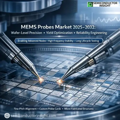
Top MEMS Probes Market Trends: Advancing Semiconductor Testing and Nanotechnology Research
At the heart of every advanced semiconductor lies a moment of truth testing. Before chips reach smartphones, vehicles, data centres, or medical devices, they must pass through microscopic contact points that verify performance under extreme precision. This is where MEMS probes operate, often unnoticed, yet absolutely essential.
MEMS probes market is evolving alongside the semiconductor industry’s relentless push toward smaller nodes, higher frequencies, and tighter tolerances. What was once a supporting component has now become a critical enabler of yield, reliability, and cost efficiency in wafer-level testing.
Why Testing Has Become the Bottleneck and the Opportunity
As chip architectures become denser and more complex, traditional probe technologies are struggling to keep pace. In high-volume fabs, even marginal improvements in probe accuracy can translate into significant yield gains. This makes MEMS probes not just a testing tool, but a strategic asset in semiconductor manufacturing economics.
MEMS probes address this challenge by offering:
- Extremely fine pitch alignment for advanced nodes
- Stable electrical contact at high frequencies
- Longer operational lifespans under repeated cycles
Latest Industry Updates:
November 2025: STMicroelectronics, a global leader in semiconductor solutions, has introduced the ISM6HG256X, a ground-breaking MEMS motion sensor designed to empower data-driven industrial transformation. This novel sensor offers unmatched motion tracking and event detection even in challenging industrial settings by combining dual-range accelerometers (±16g and ±256g) with a high-performance gyroscope in a single small device.
June 2025: Bosch has developed and launched the SMP290, a compact micro-electromechanical system (MEMS) sensor with an integrated Bluetooth low energy (BLE) interface for measuring tire pressure which the company states is the first of its kind on the market. One of the first completely integrated devices with a Bluetooth interface, the SMP290 is built on Bosch’s MEMS technology. All of the necessary parts for TPMS are combined in the sensor.
Design Philosophy Is Shifting from Mechanical to Micro-Engineered
One defining feature of the MEMS probes market is the move away from purely mechanical designs toward micro fabricated structures engineered at the silicon level.
Modern MEMS probes are built to:
- Minimize contact force while maintaining signal integrity
- Reduce pad damage on delicate wafers
- Deliver consistent performance across millions of touchdowns
This precision-driven approach is especially critical for advanced logic chips, memory devices, and RF components, where electrical noise or contact inconsistency can invalidate entire test batches.
Don’t Forget To Surf Our Latest Insights Here:
https://semiconductorinsight.com/report/mems-probes-market/
Where Demand Is Coming From Beyond Traditional Logic Chips
While logic and memory testing remain core demand drivers, MEMS probes are increasingly required in emerging semiconductor applications:
- Automotive electronics, where chips must be tested for extreme temperature and vibration tolerance
- 5G and RF devices, requiring stable high-frequency signal transmission
- Power semiconductors, where higher voltages demand robust probe materials
This diversification is expanding the addressable market and pushing probe suppliers to customize solutions by end-use rather than relying on standardized offerings.
Material Innovation Is Redefining Performance Limits
The performance of a MEMS probe depends heavily on material choice. Manufacturers are investing in advanced alloys and coatings that balance conductivity, durability, and elasticity.
Key material priorities include:
- Resistance to wear and oxidation
- Stable electrical characteristics over long test cycles
- Compatibility with fine-pitch and low-k dielectric pads
These material-level innovations are often invisible to end users but play a decisive role in reducing probe replacement frequency and overall test cost per wafer.
A Market Shaped by Customization, Not Commoditization
Unlike many semiconductor components, MEMS probes are rarely off-the-shelf products. Each probe card is typically designed around:
- Specific wafer layouts
- Target node sizes
- Electrical and thermal test requirements
This customization-heavy model favors suppliers with strong engineering capabilities and close collaboration with fabs and test equipment manufacturers. As a result, competition in the MEMS probes market is less about price and more about technical partnership.
Reliability Expectations Are Rising Sharply
Chipmakers now expect probe solutions that can operate with:
- Minimal signal drift over extended test runs
- Low maintenance downtime
- Predictable performance across large wafer volumes
Failure at the probe level can halt entire test lines, making reliability a non-negotiable purchasing criterion. This has raised qualification standards and lengthened supplier on boarding cycles, favoring experienced and technically proven vendors.
Manufacturing Scale Meets Microscopic Accuracy
Scaling MEMS probe production is not straightforward. Maintaining micron-level accuracy while increasing output volume requires:
- Advanced lithography and etching control
- Tight process repeatability
- Robust quality inspection systems
Manufacturers capable of balancing scale with precision are better positioned to serve leading-edge fabs, especially as global semiconductor capacity continues to expand.
How the Market Is Quietly Aligning with Long-Term Semiconductor Trends?
The MEMS probes market is indirectly shaped by broader industry forces:
- Continued node shrinkage
- Increased wafer-level testing
- Rising emphasis on test efficiency to manage fab costs
As chips become more valuable per wafer, the tolerance for testing errors shrinks. This structural reality ensures sustained relevance for MEMS probes, even during cyclical slowdowns in semiconductor demand.
What This Means for the Market Going Forward?
The MEMS probes market is not driven by hype or short-term volume spikes. Instead, it grows through:
- Technological necessity
- Performance-driven procurement
- Deep integration into semiconductor testing workflows
Its future lies in precision, customization, and reliability qualities that become more valuable as chips themselves grow more complex.
In many ways, MEMS probes represent the silent backbone of semiconductor progress: rarely visible, but impossible to replace.

Comments (0)